 | –≠–ª–µ–∫—Ç—Ä–æ–Ω–Ω—ã–π –∫–æ–º–ø–æ–Ω–µ–Ω—Ç: ICS9FG107 | –°–∫–∞—á–∞—Ç—å:  PDF PDF  ZIP ZIP |

Integrated
Circuit
Systems, Inc.
ICS9FG107
0863C--11/22/04
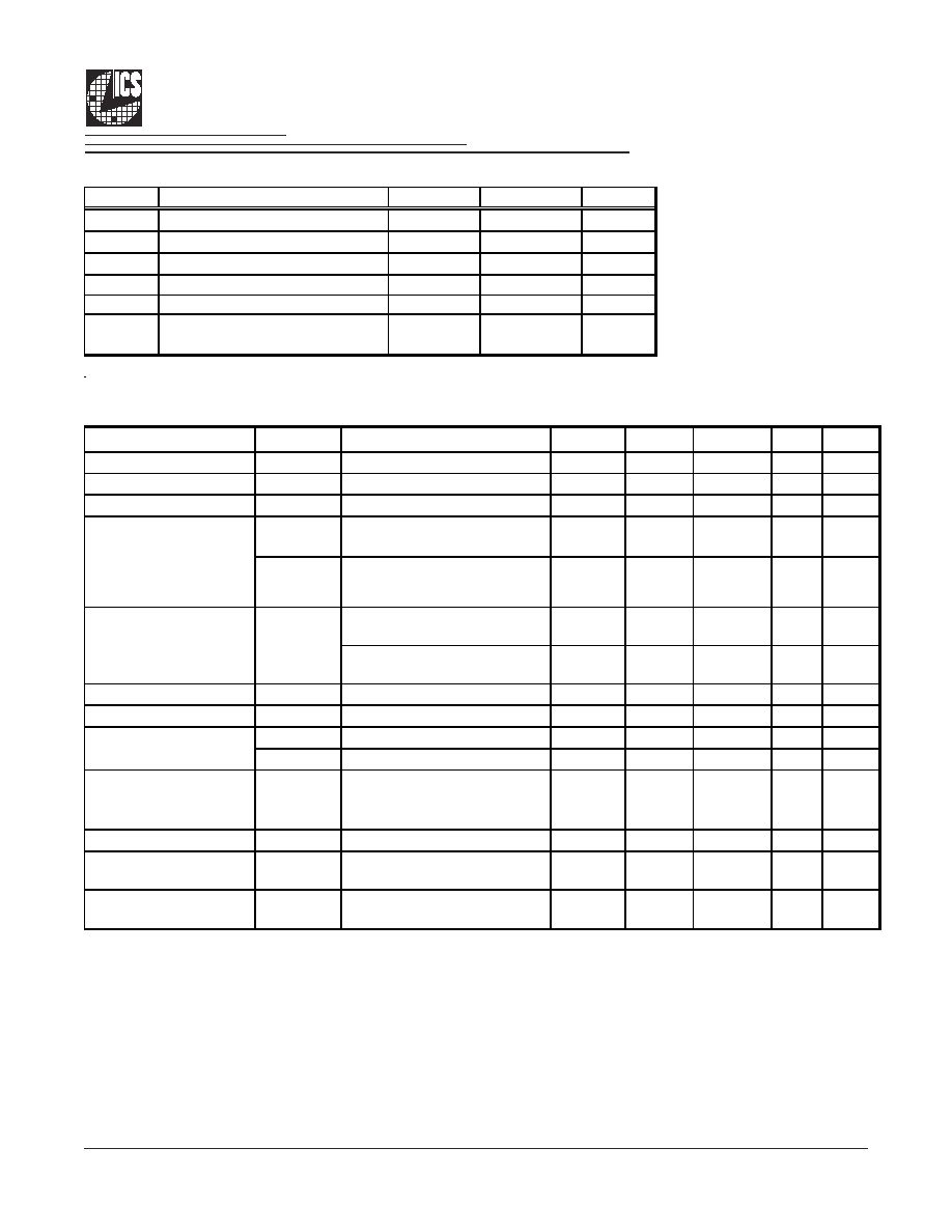
Pin Configuration
Recommended Application:
Frequency Timing Generator for Differential CPU, PCI Express
& SATA clocks
Features:
∑
Generates common CPU/PCI Express frequencies from
14.318 MHz or 25 MHz
∑
Crystal or reference input
∑
7 - 0.7V current-mode differential output pairs
∑
3 - 33MHz PCI outputs
∑
1 - REFOUT
∑
Supports Serial-ATA at 100 MHz
∑
Two spread spectrum modes: 0 to -0.5 downspread and
+/-0.25% centerspread
∑
Unused inputs may be disabled in either driven or Hi-Z
state for power management.
Key Specifications:
∑
Output cycle-to-cycle jitter for DIF outputs < 50 ps (<85ps
@ 266 MHz)
∑
Output to output skew for DIF outputs < 85 ps
∑
+/-300 ppm frequency accuracy on output clocks
Programmable FTG for Differential CPU, PCI Express* & SATA Clocks
48-pin SSOP & TSSOP
XIN/CLKIN
1
48 VDDA
X2
2
47 GNDA
VDD
3
46 IREF
GND
4
45 *DWNSPRD#
*FS2/REFOUT
5
44 **FS1
GND
6
43 *OE_0
*FS0/PCICLK_F
7
42 DIF_0
PCICLK0
8
41 DIF_0#
PCICLK1
9
40 VDD
VDD 10
39 DIF_1
**OE_6 11
38 DIF_1#
DIF_6 12
37 **OE_1
DIF_6# 13
36 VDD
VDD 14
35 GND
GND 15
34 **OE_2
**OE_5 16
33 DIF_2
DIF_5 17
32 DIF_2#
DIF_5# 18
31 VDD
VDD 19
30 DIF_3
DIF_4 20
29 DIF_3#
DIF_4# 21
28 *OE_3
*OE_4 22
27 **SEL14M_25M#
SDATA 23
26 *SPREAD
SCLK 24
25 DIF_STOP#
Notes:
Pins preceeded by * have 120 Kohm pull DOWN resistors
Pins preceeded by ** have 120 Kohm pull UP resistors
IC
S
9
F
G
1
0
7
Frequency Select Table
SEL14M_25M#
(FS3)
FS2 FS1 FS0 OUTPUT(MHz)
0
0
0
0
100.00
0
0
0
1
125.00
0
0
1
0
133.33
0
0
1
1
166.67
0
1
0
0
200.00
0
1
0
1
266.66
0
1
1
0
333.33
0
1
1
1
400.00
1
0
0
0
100.00
1
0
0
1
125.00
1
0
1
0
133.33
1
0
1
1
166.67
1
1
0
0
200.00
1
1
0
1
266.66
1
1
1
0
333.33
1
1
1
1
400.00
*Other names and brands may be claimed as the property of others.

2
Integrated
Circuit
Systems, Inc.
ICS9FG107
0863C--11/22/04
Pin Description
PIN
#
PIN NAME
PIN TYPE
DESCRIPTION
1
XIN/CLKIN
IN
Crystal input or Reference Clock input
2
X2
OUT
Crystal output, Nominally 14.318MHz
3
VDD
PWR
Power supply, nominal 3.3V
4
GND
PWR
Ground pin.
5
*FS2/REFOUT
I/O
Frequency select latch input pin / Reference clock output
6
GND
PWR
Ground pin.
7
*FS0/PCICLK_F
I/O
Frequency select latch input pin / 3.3V PCI free running clock output.
8
PCICLK0
OUT
PCI clock output.
9
PCICLK1
OUT
PCI clock output.
10
VDD
PWR
Power supply, nominal 3.3V
11
**OE_6
IN
Active high input for enabling outputs.
0 = tri-state outputs, 1= enable outputs
12
DIF_6
OUT
0.7V differential true clock outputs
13
DIF_6#
OUT
0.7V differential complement clock outputs
14
VDD
PWR
Power supply, nominal 3.3V
15
GND
PWR
Ground pin.
16
**OE_5
IN
Active high input for enabling outputs.
0 = tri-state outputs, 1= enable outputs
17
DIF_5
OUT
0.7V differential true clock outputs
18
DIF_5#
OUT
0.7V differential complement clock outputs
19
VDD
PWR
Power supply, nominal 3.3V
20
DIF_4
OUT
0.7V differential true clock outputs
21
DIF_4#
OUT
0.7V differential complement clock outputs
22
*OE_4
IN
Active high input for enabling outputs.
0 = tri-state outputs, 1= enable outputs
23
SDATA
I/O
Data pin for SMBus circuitry, 5V tolerant.
24
SCLK
IN
Clock pin of SMBus circuitry, 5V tolerant.

3
Integrated
Circuit
Systems, Inc.
ICS9FG107
0863C--11/22/04
Pin Description (Continued)
PIN
#
PIN NAME
PIN TYPE
DESCRIPTION
25
DIF_STOP#
IN
Active low input to stop differential output clocks.
26
*SPREAD
IN
Asynchronous, active high input, with internal 120Kohm pull-up
resistor, to enable spread spectrum functionality.
27
**SEL14M_25M#
IN
Select 14.31818 MHz or 25 Mhz input frequency. 1 = 14.31818 MHz,
0 = 25 MHz
28
*OE_3
IN
Active high input for enabling outputs.
0 = tri-state outputs, 1= enable outputs
29
DIF_3#
OUT
0.7V differential complement clock outputs
30
DIF_3
OUT
0.7V differential true clock outputs
31
VDD
PWR
Power supply, nominal 3.3V
32
DIF_2#
OUT
0.7V differential complement clock outputs
33
DIF_2
OUT
0.7V differential true clock outputs
34
**OE_2
IN
Active high input for enabling outputs.
0 = tri-state outputs, 1= enable outputs
35
GND
PWR
Ground pin.
36
VDD
PWR
Power supply, nominal 3.3V
37
**OE_1
IN
Active high input for enabling outputs.
0 = tri-state outputs, 1= enable outputs
38
DIF_1#
OUT
0.7V differential complement clock outputs
39
DIF_1
OUT
0.7V differential true clock outputs
40
VDD
PWR
Power supply, nominal 3.3V
41
DIF_0#
OUT
0.7V differential complement clock outputs
42
DIF_0
OUT
0.7V differential true clock outputs
43
*OE_0
IN
Active high input for enabling outputs.
0 = tri-state outputs, 1= enable outputs
44
**FS1
I/O
Frequency select latch input pin / 3.3V 66.66MHz clock output.
45
*DWNSPRD#
IN
3.3V input that selects spread mode. This input is not latched at
power up.
0 = Down Spread, 1 = Center Spread
46
IREF
OUT
This pin establishes the reference current for the differential current-
mode output pairs. This pin requires a fixed precision resistor tied to
ground in order to establish the appropriate current. 475 ohms is the
standard value.
47
GNDA
PWR
Ground pin for the PLL core.
48
VDDA
PWR
3.3V power for the PLL core.
Pins preceeded by * have 120 Kohm pull DOWN resistors
Pins preceeded by ** have 120 Kohm pull UP resistors

4
Integrated
Circuit
Systems, Inc.
ICS9FG107
0863C--11/22/04
ICS9FG107 is a Frequency Timing Generator that provides 7 differential output pairs that are compliant to the Intel CK409/
CK410 specification. It provides support for PCI-Express, next generation I/O, and SATA. The part synthesizes several output
frequencies from either a 14.31818 Mhz crystal or a 25 MHz crystal. The device can also be driven by a reference input clock
instead of a crystal. It provides outputs with cycle-to-cycle jitter of less than 85 ps and output-to-output skew of less than 85 ps.
ICS9FG107 also provides a copy of the reference clock and 3 33 MHz PCI output clocks. Frequency selection can be
accomplished via strap pins or SMBus control.
General Description
Block Diagram
Power Groups
I REF
Programmable
Spread
PLL1
Programmable
Frequency
Dividers
X2
XIN/CLKIN
SDATA
SCLK
REFOUT
DIF_STOP#
SEL14M_25M#
SPREAD
DWNSPRD#
OE (6:0)
FS (2:0)
Control
Logic
DIF (6:0)
DIF# (6:0)
PCICLK (1:0)
PCICLK_F
VDD
GND
3
4
10
6
14,19,31,36,40
15,35
N/A
47
48
47
IREF
Analog VDD & GND for PLL Core
Description
Pin Number
REFOUT, Digital Inputs, SMBus
DIF Outputs
PCI Outputs
5
Integrated
Circuit
Systems, Inc.
ICS9FG107
0863C--11/22/04
Absolute Max
Symbol
Parameter
Min
Max
Units
VDD_A
3.3V Core Supply Voltage
V
DD
+ 0.5V
V
VDD_In
3.3V Logic Input Supply Voltage
GND - 0.5
V
DD
+ 0.5V
V
Ts
Storage Temperature
-65
150
∞
C
Tambient
Ambient Operating Temp
0
70
∞C
Tcase Case
Temperature
115
∞C
ESD prot
Input ESD protection
human body model
2000
V
Electrical Characteristics - Input/Supply/Common Output Parameters
T
A
= 0 - 70∞C; Supply Voltage V
DD
= 3.3 V +/-5%
PARAMETER
SYMBOL
CONDITIONS
MIN
TYP
MAX
UNITS NOTES
Input High Voltage
V
IH
3.3 V +/-5%
2
V
DD
+ 0.3
V
Input Low Voltage
V
IL
3.3 V +/-5%
V
SS
- 0.3
0.8
V
Input High Current
I
IH
V
IN
= V
DD
-5
5
uA
I
IL1
V
IN
= 0 V; Inputs with no pull-
up resistors
-5
uA
I
IL2
V
IN
= 0 V; Inputs with pull-up
resistors
-200
uA
Full Active, C
L
= Full load;
f = 400 MHz
250
mA
Full Active, C
L
= Full load;
f = 100 MHz
200
mA
Input Frequency
3
F
i
V
DD
= 3.3 V
14
25
MHz
3
Pin Inductance
1
L
pin
7
nH
1
C
IN
Logic Inputs
1.5
5
pF
1
C
OUT
Output pin capacitance
6
pF
1
Clk Stabilization
1,2
T
STAB
From V
DD
Power-Up and after
input clock stabilization to 1st
clock
1.8
ms
1,2
Modulation Frequency
f
MOD
Triangular Modulation
30
40
kHz
1
DIF output enable
t
DIFOE
DIF output enable after
DIF_Stop# de-assertion
10
ns
1
Input Rise and Fall times
t
R
/t
F
20% to 80% of VDD
5
ns
1
1
Guaranteed by design and characterization, not 100% tested in production.
2
See timing diagrams for timing requirements.
3
Input frequency should be measured at the REFOUT pin and tuned to ideal 14.31818MHz or 25 MHz to meet
ppm frequency accuracy on PLL outputs.
Input/Output
Capacitance
1
Input Low Current
I
DD3.3OP
Operating Supply Current