
Integrated
Circuit
Systems, Inc.
ICS9S857
Preliminary Product Preview
Low-Voltage 10-Bit FET BUS Switch With
Internal Pulldown Resistors
9S857 Rev A 7/31/00
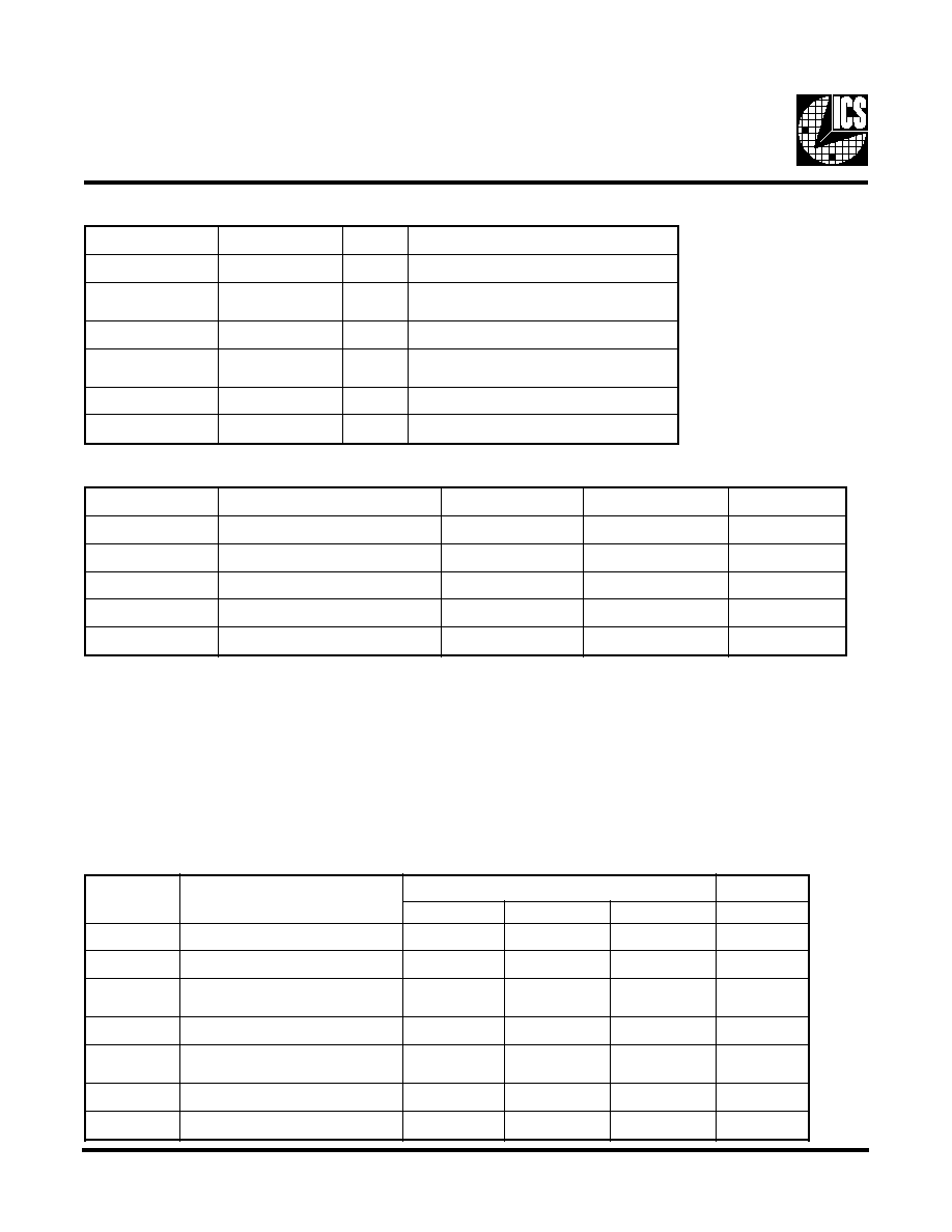
Pin Configuration
24-Pin TSSOP
Product Features:
Full DDR solution provided when used with
ICSSSTV16857 and ICS93857
Enable signal is SSTL_2 compatible
Flow-through architecture optimizes PCB layout
Designed for use with 200 Mbit/s Double Data-Rate
(DDR) SDRAM applications
Switch On-state restance is designed to eliminate series
resistor to DDR SDRAM
Internal 10W pulldown resistors to ground on B port
Internal 50W pullup resistor on Output-Enable
(OE#) input
Latch-up perfromance exceeds 100 mA per JESD 78,
Class II
Available in 24 pin TSSOP package
VREF
A1
A2
A3
A4
A5
A6
A7
A8
A9
A10
GND
VDD
OE#
B1
B2
B3
B4
B5
B6
B7
B8
B9
B10
ICS9S857
1
2
3
4
5
6
7
8
9
10
11
12
24
23
22
21
20
19
18
17
16
15
14
13
V
DD
OE#
A1
B1
22
2
13
11
1
23
A10
B10
VREF
R
INT
R
INT
SW
SW
(OE#)
A
B
Logic Diagram (Positive Logic)
Simplified Shcematic, Each FET Switch
Function Table
T
U
P
N
I
#
E
O
N
O
I
T
C
N
U
F
L
H
t
r
o
p
B
=
t
r
o
p
A
t
c
e
n
n
o
c
s
i
D
PRODUCT PREVIEW documents contain information on new
products in the sampling or preproduction phase of development.
Characteristic data and other specifications are subject to change
without notice.
2
ICS9S857
Preliminary Product Preview
Pin Descriptions
R
E
B
M
U
N
N
I
P
E
M
A
N
N
I
P
E
P
Y
T
N
O
I
T
P
I
R
C
S
E
D
1
F
E
R
V
T
U
O
e
g
a
t
l
o
v
t
u
p
t
u
o
e
c
n
e
r
e
f
e
R
,
9
,
8
,
7
,
6
,
5
,
4
,
3
,
2
1
1
,
0
1
0
1
A
-
1
A
N
I
s
t
u
p
n
I
2
1
D
N
G
R
W
P
d
n
u
o
r
G
,
8
1
,
9
1
,
0
2
,
1
2
,
2
2
,
3
1
,
4
1
,
5
1
,
6
1
,
7
1
0
1
B
-
1
B
T
U
O
s
t
u
p
t
u
O
3
2
#
E
O
N
I
e
l
b
a
n
E
t
u
p
t
u
O
4
2
D
D
V
R
W
P
)
V
6
.
3
(
y
l
p
p
u
s
r
e
w
o
P
L
O
B
M
Y
S
R
E
T
E
M
A
R
A
P
S
N
O
I
T
I
D
N
O
C
G
N
I
T
A
R
T
I
N
U
V
D
D
e
g
a
t
l
o
V
y
l
p
p
u
s
C
D
6
.
4
+
o
t
5
.
0
-
V
I
K
I
t
n
e
r
r
u
c
p
m
a
l
c
t
u
p
n
i
C
D
V
O
/
I
0
<
0
5
-
A
m
V
I
)
y
l
n
o
#
E
O
(
e
g
n
a
r
e
g
a
t
l
o
v
t
u
p
n
i
C
D
2
V
D
D
5
.
0
+
V
T
g
t
s
e
g
n
a
r
e
r
u
t
a
r
e
p
m
e
t
e
g
a
r
o
t
S
0
5
1
o
t
5
6
-
C
°
V
I
)
#
E
O
t
p
e
c
x
e
(
e
g
a
t
l
o
v
t
u
p
n
i
C
D
2
6
.
4
o
t
5
.
0
-
V
Absolute Maximum Ratings
Notes:
1.
Stresses beyond those listed may cause permanent damage to the device. These are stress ratings only and functional
operation of the device at these or any other conditions beyond those indicated under " recommended operating
conditions' is not implied. Exposure to absolute-maximum-rated conditions for extended periods may affect device
reliability.
2.
The input and output negative-voltage ratings may be exceeded if the input and output clamp-current ratings
are observed.
3.
The package thermal impedance is calculated in accordance with JESD 51.
L
O
B
M
Y
S
R
E
T
E
M
A
R
A
P
S
T
I
M
I
L
N
I
M
P
Y
T
X
A
M
T
I
N
U
V
D
D
e
g
a
t
l
o
V
y
l
p
p
u
s
C
D
3
3
.
3
6
.
3
V
V
F
E
R
V
x
8
3
.
0
(
e
g
a
t
l
o
v
e
c
n
e
r
e
f
e
R
D
D
)
5
1
.
1
5
2
.
1
5
3
.
1
V
V
H
I
t
u
p
n
i
l
e
v
e
l
-
h
g
i
h
C
A
V
F
E
R
+
V
m
0
5
3
V
V
L
I
e
g
a
t
l
o
v
t
u
p
n
i
l
e
v
e
l
-
w
o
l
C
A
V
F
E
R
V
m
0
5
3
-
V
V
H
I
e
g
a
t
l
o
v
t
u
p
n
i
l
e
v
e
l
-
h
g
i
h
C
D
V
F
E
R
+
V
m
0
8
1
V
V
L
I
e
g
a
t
l
o
v
t
u
p
n
i
l
e
v
e
l
-
w
o
l
C
D
V
F
E
R
V
m
0
8
1
-
V
T
b
m
a
e
g
n
a
r
e
r
u
t
a
r
e
p
m
e
t
r
i
a
-
e
e
r
f
g
n
i
t
a
r
e
p
O
0
5
8
+
C
°
Recommended Operating Condidions
3
ICS9S857
Preliminary Product Preview
Ordering Information
ICS9S857yGT
Designation for tape and reel packaging
Pattern Number (2 or 3 digit number for parts with ROM code patterns)
Package Type
G=TSSOP
Revision Designator (will not correlate with datasheet revision)
Device Type (consists of 3 or 4 digit numbers)
Prefix
ICS, AV = Standard Device
Example:
ICS XXXX y G - PPP - T
MIN
MAX
MIN
MAX
A
-
1.20
-
0.047
A1
0.05
0.15
.002
.006
A2
0.80
1.05
.032
.041
b
0.17
0.27
.007
.011
c
0.09
0.20
.0035
.008
D
E
E1
4.30
4.50
.169
.177
e
0.50 BASIC
0.020 BASIC
L
0.45
0.75
.018
.030
N
0°
8°
0°
8°
aaa
-
0.10
-
.004
VARIATIONS
MIN
MAX
MIN
MAX
20
4.90
5.10
.193
.201
24
6.40
6.60
.252
.260
28
7.70
7.90
.303
.311
30
7.70
7.90
.303
.311
36
9.60
9.80
.378
.386
38
9.60
9.80
.378
.386
44
10.90
11.10
.429
.437
50
12.40
12.60
.488
.496
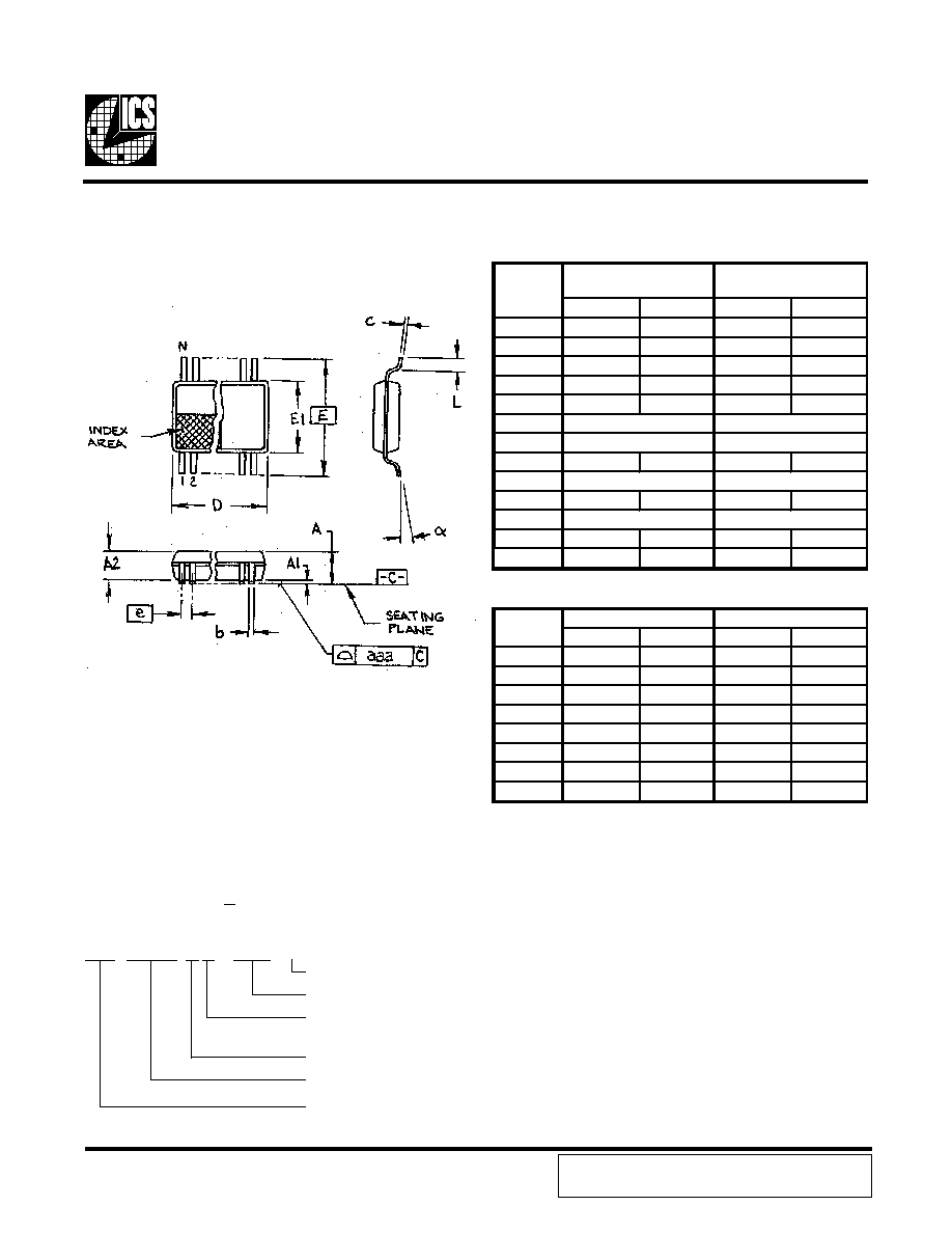
MO-153 JEDEC
Doc.# 10-0036
7/6/00 Rev B
SYMBOL
SEE VARIATIONS
SEE VARIATIONS
In Millimeters
COMMON DIMENSIONS
In Inches
COMMON DIMENSIONS
SEE VARIATIONS
6.40 BASIC
0.252 BASIC
N
D mm.
D (inch)
SEE VARIATIONS
4.40 mm. Body, 0.50 mm. pitch TSSOP
(173 mil)
(0.020 mil)
PRODUCT PREVIEW documents contain information on new
products in the sampling or preproduction phase of development.
Characteristic data and other specifications are subject to change
without notice.