Äîêóìåíòàöèÿ è îïèñàíèÿ www.docs.chipfind.ru
ICSLV810
MDS LV810 F
1
Revision 101305
Integrated Circuit Systems, Inc.
525 Race Street, San Jose, CA 95126
tel (408) 297-1201
www.icst.com
Buffer/Clock Driver
Description
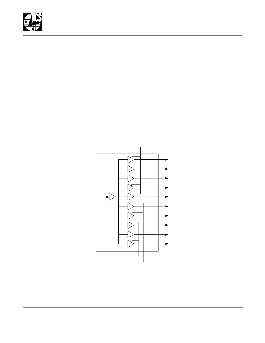
The ICSLV810 is a low skew 1.5 V to 2.5 V, 1:10 fanout
buffer. This device is specifically designed for data
communications clock management. The large fanout
from a single input line reduces loading on the input
clock. The TTL level outputs reduce noise levels on the
part. Typical applications are clock and signal
distribution.
Features
·
Packaged in 20-pin QSOP/SSOP
·
Split 1:10 fanout Buffer
·
Maximum skew between outputs of different
packages 0.75 ns
·
Max propagation delay of 3.8 ns
·
Operating voltage of 1.5 V to 2.5 V on Bank A
·
Operating voltage of 1.5 V to 2.5 V on Banks B and C
·
Advanced, low power, CMOS process
·
Industrial temperature range -40
° C to +85° C
·
3.3 V tolerant input when VDDA=2.5 V
·
Available in Pb (lead) free packaging
Block Diagram
CLK 1
CLK 2
CLK 3
CLK 4
CLK 5
CLK 6
CLK 7
CLK 8
CLK 9
CLK 10
VDDA
VDDB
CLKIN
VDDC
Buffer/Clock Driver
MDS LV810 F
2
Revision 101305
Integrated Circuit Systems, Inc.
525 Race Street, San Jose, CA 95126
tel (408) 297-1201
www.icst.com
ICSLV810
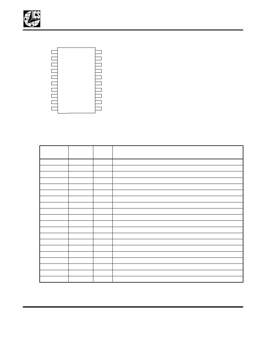
Pin Assignment
Pin Descriptions
20 pin (150mil) SSOP
CLKIN
GND
CLK 1
VDDA
CLK 2
GND
CLK 3
CLK 4
VDDA
GND
GND
GND
VDDB
VDDC
CLK 5
CLK 6
CLK 7
CLK 8
CLK 9
CLK 10
1
2
3
4
5
6
7
8
9
10
11
12
13
14
15
16
17
18
19
20
Pin
Number
Pin
Name
Pin
Type
Pin Description
1
CLKIN
Input
Clock input.
2
GND
Power
Connect to ground.
3
CLK1
Output
Clock output.
4
VDDA
Power
Connect to +1.5 - +2.5 V.
5
CLK2
Output
Clock output.
6
GND
Power
Connect to ground.
7
CLK3
Output
Clock output.
8
VDDA
Power
Connect to +1.5 - +2.5 V.
9
CLK4
Output
Clock output.
10
GND
Power
Connect to ground.
11
CLK5
Output
Clock output.
12
CLK6
Output
Clock output.
13
GND
Power
Connect to ground.
14
CLK7
Output
Clock output.
15
VDDC
Power
Connect to +1.5 - 2.5 V.
16
CLK8
Output
Clock output.
17
GND
Power
Connect to ground.
18
CLK9
Output
Clock output.
19
CLK10
Output
Clock output.
20
VDDB
Power
Connect to +1.5 - 2.5 V.
Buffer/Clock Driver
MDS LV810 F
3
Revision 101305
Integrated Circuit Systems, Inc.
525 Race Street, San Jose, CA 95126
tel (408) 297-1201
www.icst.com
ICSLV810
External Components
The ICSLV810 requires a minimum number of external
components for proper operation.
Decoupling Capacitors
Decoupling capacitors of 0.01µF must be connected
between VDD and GND, as close to these pins as
possible. For optimum device performance, the
decoupling capacitors should be mounted on the
component side of the PCB. Avoid the use of vias in the
decoupling circuit.
Series Termination Resistor
When the PCB trace between the clock outputs and the
loads are over 1 inch, series termination should be
used. To series terminate a 50
trace (a commonly
used trace impedance) place a 33
resistor in series
with the clock line, as close to the clock output pin as
possible. The nominal impedance of the clock output is
20
.
PCB Layout Recommendations
For optimum device performance and lowest output
phase noise, the following guidelines should be
observed.
1) The 0.01µF decoupling capacitors should be
mounted on the component side of the board as close
to the VDD pins as possible. No vias should be used
between the decoupling capacitors and VDD pins. The
PCB trace to VDD pin should be kept as short as
possible, as should the PCB trace to the ground via.
2) To minimize EMI the 33
series termination resistor,
if needed, should be placed close to the clock output.
Absolute Maximum Ratings
Stresses above the ratings listed below can cause permanent damage to the ICSLV810. These ratings,
which are standard values for ICS commercially rated parts, are stress ratings only. Functional operation of
the device at these or any other conditions above those indicated in the operational sections of the
specifications is not implied. Exposure to absolute maximum rating conditions for extended periods can
affect product reliability. Electrical parameters are guaranteed only over the recommended operating
temperature range.
Recommended Operation Conditions
Item
Rating
Supply Voltage, VDD MAX
7 V
All Inputs and Outputs
-0.5 V to VDDA + 1.2 V
Ambient Operating Temperature
-40 to +85
°C
Storage Temperature
-65 to +150
°C
Junction Temperature
125
°C
Soldering Temperature
260
°C
Parameter
Min.
Typ.
Max.
Units
Ambient Operating Temperature
-40
+85
°C
Power Supply Voltage (measured with respect to GND), VDDA
1.425
2.625
V
Power Supply Voltage (measured with respect to GND), VDDB
1.425
2.625
V
Power Supply Voltage (measured with respect to GND), VDDC
1.425
2.625
V
Buffer/Clock Driver
MDS LV810 F
4
Revision 101305
Integrated Circuit Systems, Inc.
525 Race Street, San Jose, CA 95126
tel (408) 297-1201
www.icst.com
ICSLV810
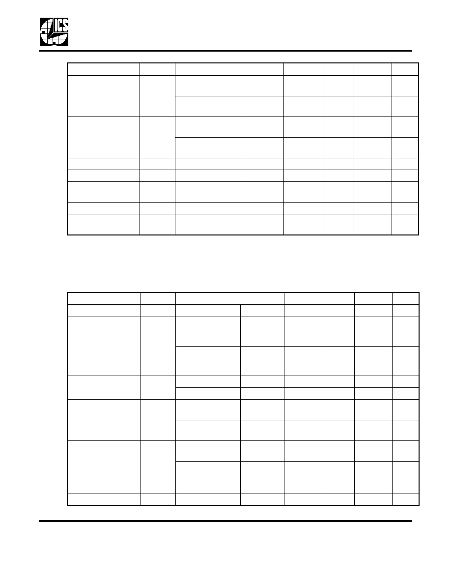
DC Electrical Characteristics--CLKIN and Bank A
VDDA = 2.5 V, Ambient Temperature -40
° C to +85° C
Note1: This parameter is not tested, guaranteed by design.
DC Electrical Characteristics--Bank B
VDDB = 2.5 V, Ambient Temperature -40
° C to +85° C, unless otherwise noted
Parameter
Symbol
Conditions
Min.
Typ.
Max.
Units
Operating Voltage
VDDA
1.425
2.625
V
Quiescent Power Supply
Current
IDDA
No Load
F = 40 MHz
15
mA
Short Circuit Current
I
OS
CLK 1 - 5
±80
mA
Input High Voltage,
CLKIN
V
IH
Guaranteed
Logic Level
High
1.6
V
Input Low Voltage,
CLKIN
V
IL
Guaranteed
Logic Level Low
0.8
V
Output High Voltage
V
OH
VIN = VIH or
VIL
I
OH
=
-7 mA
1.8
V
Output Low Voltage
V
OL
VIN = VIH or
VIL
I
OL =
12 mA
0.4
V
Input High Current
I
IH
VDD = max
VIN = 2.4 V
1
µA
Input Low Current
I
IL
VDD = max
VIN = 0.5 V
-1
µA
Input High Current
I
I
VDD = max
VIN = VDD
(max)
20
µA
Input Capacitance
C
IN
VIN
= 0V, Note1
5
6.0
pF
Output Capacitance
C
OUT
V
OUT
= 0V,
Note1
5.5
8.0
pF
Parameter
Symbol
Conditions
Min.
Typ.
Max.
Units
Operating Voltage
VDDB
1.425
2.625
V
Quiescent Power
Supply Current
IDDB
VDDB = 2.5 V
No Load
F = 40 MHz
7
mA
VDDB = 1.5 V
No Load
F = 40 MHz
3
mA
Short Circuit
Current
I
OS
VDDB = 1.5 V
CLK8-10
±35
mA
VDDB = 2.5 V
CLK8-10
±80
mA
Buffer/Clock Driver
MDS LV810 F
5
Revision 101305
Integrated Circuit Systems, Inc.
525 Race Street, San Jose, CA 95126
tel (408) 297-1201
www.icst.com
ICSLV810
Note1: This parameter is not tested, guaranteed by design.
DC Electrical Characteristics--Bank C
VDDC = 2.5 V, Ambient Temperature -40
° C to +85° C, unless otherwise noted
Output High Voltage
V
OH
VDDB = 1.5 V
VIN = VIH or VIL
I
OH
=
-7 mA
1.1
V
VDDB = 2.5 V
VIN = VIH or VIL
I
OH
=
-7 mA
1.8
V
Output Low Voltage
V
OL
VDDB = 1.5 V
VIN = VIH or VIL
I
OL =
12 mA
0.42
V
VDDB = 2.5 V
VIN = VIH or VIL
I
OL =
12 mA
0.4
V
Input High Current
I
IH
VDDB = max
1
µA
Input Low Current
I
IL
VDDB = max
-1
µA
Input High Current
I
I
VDDB = max,
VIN = VDD (max)
20
µA
Input Capacitance
C
IN
VIN
= 0V, Note1
5
6.0
pF
Output Capacitance
C
OUT
V
OUT
= 0V,
Note 1
5.5
8.0
pF
Parameter
Symbol
Conditions
Min.
Typ.
Max.
Units
Operating Voltage
VDDC
1.425
2.625
V
Quiescent Power
Supply Current
IDDC
VDDC = 2.5 V
No Load
F = 40 MHz
3
mA
VDDC = 1.5 V
No Load
F = 40 MHz
2
mA
Short Circuit Current
I
OS
VDDC = 1.5 V
CLK6-7
±35
mA
VDDC = 2.5 V
CLK6-7
±80
mA
Output High Voltage
V
OH
VDDC = 1.5 V
VIN = VIH or VIL
I
OH
=
-7 mA
1.1
V
VDDC = 2.5 V
VIN = VIH or VIL
I
OH
=
-7 mA
1.8
V
Output Low Voltage
V
OL
VDDC = 1.5 V
VIN = VIH or VIL
I
OL =
12 mA
0.42
V
VDDC = 2.5 V
VIN = VIH or VIL
I
OL =
12 mA
0.4
V
Input High Current
I
IH
VDDC = max
1
µA
Input Low Current
I
IL
VDDC = max
-1
µA
Parameter
Symbol
Conditions
Min.
Typ.
Max.
Units
Document Outline