Integrated
Circuit
Systems, Inc.
ICSSSTV16857
Third party brands and names are the property of their respective owners.
16857 Rev D 07/09/01
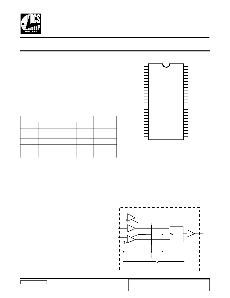
Pin Configuration
Recommended Application:
DDR Memory Modules
Product Features:
∑
Differential clock signal
∑
Meets SSTL_2 signal data
∑
Supports SSTL_2 class I & II specifications
∑
low-voltage operation
VDD = 2.3V to 2.7V
∑
48 pin TSSOP package
DDR 14-Bit Registered Buffer
Truth Table
1
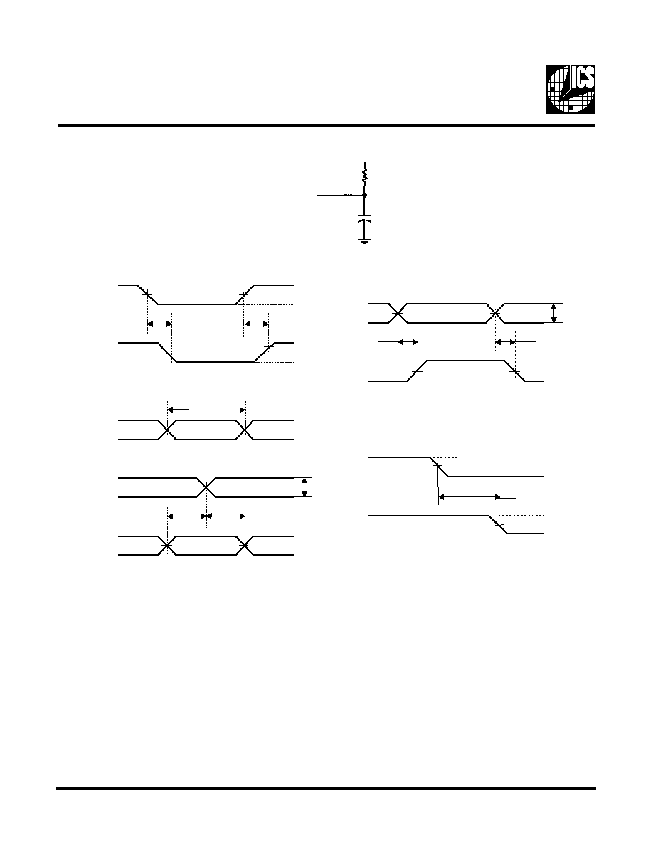
Block Diagram
Q1
Q2
GND
VDDQ
Q3
Q4
Q5
GND
VDDQ
Q6
Q7
VDDQ
GND
Q8
Q9
VDDQ
GND
Q10
Q11
Q12
VDDQ
GND
Q13
Q14
D1
D2
GND
VDD
D3
D4
D5
D6
D7
CLK#
CLK
VDD
GND
VREF
RESET#
D8
D9
D10
D11
D12
VDD
GND
D13
D14
ICSSSTV16857
1
2
3
4
5
6
7
8
9
10
11
12
13
14
15
16
17
18
19
20
21
22
23
24
48
47
46
45
44
43
42
41
40
39
38
37
36
35
34
33
32
31
30
29
28
27
26
25
CLK
CLK#
38
39
48
35
34
D1
VREF
RESET#
To 13 Other Channels
Q1
1
CLK
R
D1
Notes:
1.
H = High Signal Level
L = Low Signal Level
= Transition LOW-to-HIGH
= Transition HIGH -to LOW
X = Irrelevant
2.
Output level before the indicated
steady state input conditions were
established.
s
t
u
p
n
I
s
t
u
p
t
u
O
Q
#
T
E
S
E
R
K
L
C
#
K
L
C
D
Q
L
r
o
X
g
n
i
t
a
o
l
F
r
o
X
g
n
i
t
a
o
l
F
r
o
X
g
n
i
t
a
o
l
F
L
H
H
H
H
L
L
H
H
r
o
L
H
r
o
L
X
Q
0
)
2
(
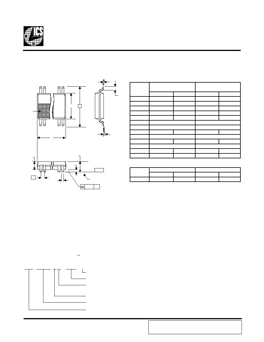
48-Pin TSSOP & TVSOP
6.10 mm. Body, 0.50 mm. pitch = TSSOP
4.40 mm. Body, 0.40 mm. pitch = TSSOP (TVSOP)
ICS reserves the right to make changes in the device data identified in
this publication without further notice. ICS advises its customers to
obtain the latest version of all device data to verify that any
information being relied upon by the customer is current and accurate.

2
ICSSSTV16857
Third party brands and names are the property of their respective owners.
General Description
Pin Configuration
The 14-bit ICSSTV16857 is a universal bus driver designed for 2.3V to 2.7V VDD operation and SSTL_2 I/O Levels
except for the RESET# input which is LVCMOS.
Data flow from D to Q is controlled by the differential clock, CLK, CLK# and RESET#. Data is triggered on the
positive edge of CLK. CLK# must be used to maintain noise margins. RESET# must be supported with LVCMOS
levels as VREF may not be stable during power-up. RESET# is asynchronous and is intended for power-up only and
when low assures that all of the registers reset to the Low State, Q outputs are low, and all input receivers, data and
clock are switched off.
R
E
B
M
U
N
N
I
P
E
M
A
N
N
I
P
E
P
Y
T
N
O
I
T
P
I
R
C
S
E
D
,
8
1
,
9
1
,
0
2
,
3
2
,
4
2
,
6
,
7
,
0
1
,
1
1
,
4
1
,
5
1
1
,
2
,
5
)
1
:
4
1
(
Q
T
U
P
T
U
O
t
u
p
t
u
o
a
t
a
D
,
2
2
,
3
1
,
8
,
3
6
4
,
6
3
,
7
2
D
N
G
R
W
P
d
n
u
o
r
G
1
2
,
6
1
,
2
1
,
9
,
4
Q
D
D
V
R
W
P
e
g
a
tl
o
v
y
l
p
p
u
s
t
u
p
t
u
O
,
1
3
,
0
3
,
9
2
,
6
2
,
5
2
,
2
4
,
1
4
,
0
4
,
3
3
,
2
3
8
4
,
7
4
,
4
4
,
3
4
)
1
:
4
1
(
D
T
U
P
N
I
t
u
p
n
i
a
t
a
D
8
3
K
L
C
T
U
P
N
I
t
u
p
n
i
k
c
o
l
c
e
v
it
i
s
o
P
9
3
#
K
L
C
T
U
P
N
I
t
u
p
n
i
k
c
o
l
c
e
v
it
a
g
e
N
5
4
,
7
3
,
8
2
D
D
V
R
W
P
e
g
a
tl
o
v
y
l
p
p
u
s
e
r
o
C
4
3
#
T
E
S
E
R
T
U
P
N
I
)
w
o
l
e
v
it
c
a
(
t
e
s
e
R
5
3
F
E
R
V
T
U
P
N
I
e
g
a
tl
o
v
e
c
n
e
r
e
f
e
r
t
u
p
n
I

3
ICSSSTV16857
Third party brands and names are the property of their respective owners.
Absolute Maximum Ratings
Storage Temperature . . . . . . . . . . . . . . . . . . . . . . . ≠65∞C to +150∞C
Supply Voltage . . . . . . . . . . . . . . . . . . . . . . . . . . . . -0.5 to 3.6V
Input Voltage
1
. . . . . . . . . . . . . . . . . . . . . . . . . . . . . . . . . . . . . .
-0.5 to VDD +0.5
Output Voltage
1,2
. . . . . . . . . . . . . . . . . . . . . . . . . . . . . . . . . .
-0.5 to VDDQ +0.5
Input Clamp Current . . . . . . . . . . . . . . . . . . . . . . . ±50 mA
Output Clamp Current . . . . . . . . . . . . . . . . . . . . . ±50mA
Continuous Output Current . . . . . . . . . . . . . . . . . ±50mA
VDD, VDDQ or GND Current/Pin . . . . . . . . . . . . ±100mA
Package Thermal Impedance
3
. . . . . . . . . . . . . . . . . . . .
55∞C/W
Stresses above those listed under Absolute Maximum Ratings may cause permanent damage to the device. These ratings are
stress specifications only and functional operation of the device at these or any other conditions above those listed in the
operational sections of the specifications is not implied. Exposure to absolute maximum rating conditions for extended
periods may affect product reliability.
Notes:
1. The input and output negative voltage
ratings may be excluded if the input
and output clamp ratings are observed.
2. This current will flow only whtn the
output is in the high state level
V
0
>V
DDQ
.
3. The package thermal impedance is
calculated in accordance with
JESD 51.
Recommended Operating Conditions
PARAM ETER
M IN
TYP
M AX
UNITS
V
DD
2.3
2.5
2.7
V
DDQ
2.3
2.5
2.7
V
REF
1.15
1.25
1.35
V
TT
V
REF
-0.04
V
REF
V
REF
-0.04
V
I
Input Voltage
0
V
DD
V
IH
DC Input High Voltage
V
REF
+0.15
V
IH
AC Input High Voltage
V
REF
+0.31
V
IL
DC Input Low Voltage
V
REF
-0.15
V
IL
AC Input Low Voltage
V
REF
-0.31
V
IH
Input High Voltage Level
1.7
V
IL
Input Low Voltage Level
0.7
V
ICR
Common mode Input Range
0.97
1.53
V
ID
Differential Input Voltage
0.36
V
IX
(V
DDQ
/2) -0.2
(V
DDQ
/2)
+0.2
I
OH
-20
I
OL
20
T
A
0
70
∞C
1
Guarenteed by design, not 100% tested in production.
Operating Free-Air Temperature
RESET#
CLK, CLK#
V
Termination Voltage
Cross Point Voltage of Differential Clock
Pair
High-Level Output Current
Low-Level Output Current
Data Inputs
mA
DESCRIPTION
Supply Voltage
I/O Supply Voltage
Reference Voltage V
REF
= 0.5X V
DDQ
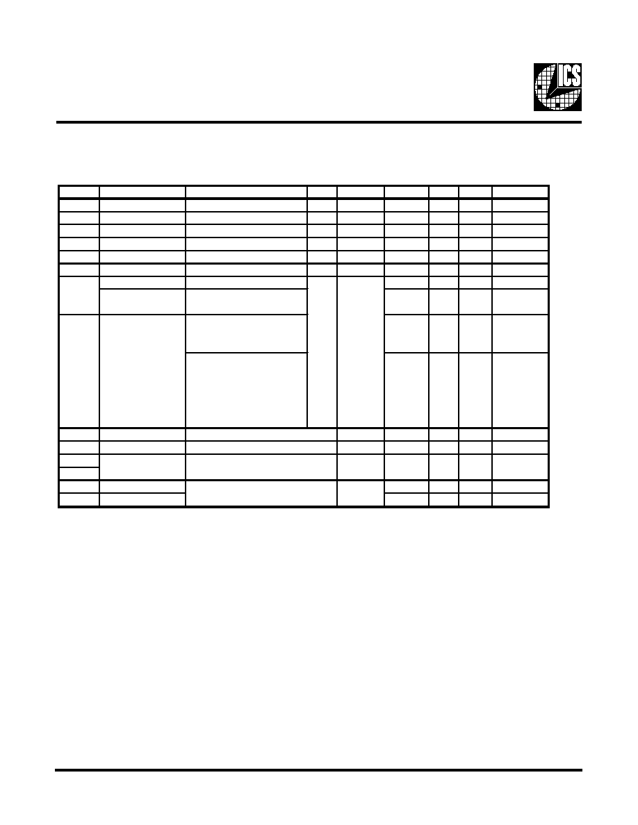
4
ICSSSTV16857
Third party brands and names are the property of their respective owners.
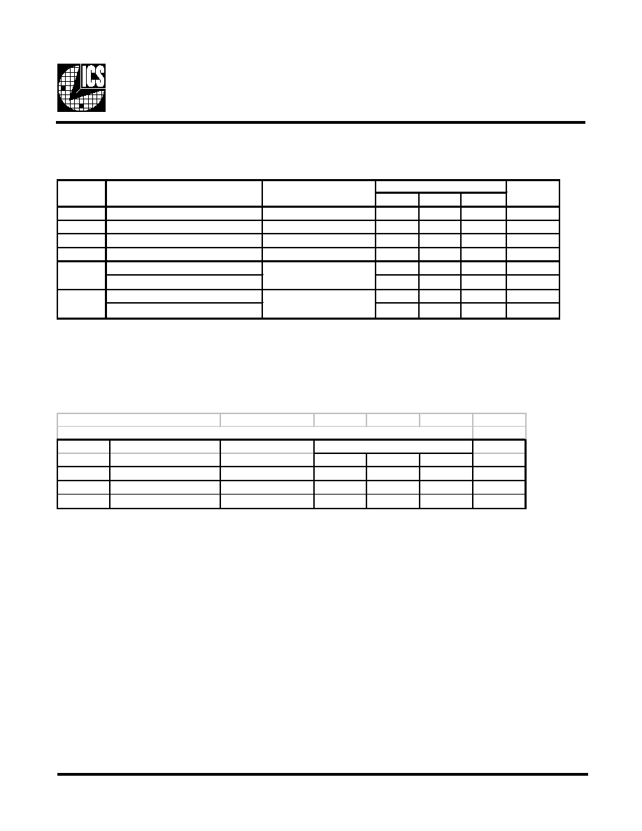
Electrical Characteristics - DC
T
A
= 0 - 70∫ C; V
DD
= 2.5 V +/-200mV, V
DDQ
=2.5V 200mV; (unless otherwise stated)
SYMBOL
PARAMETERS
CONDITIONS
VDD
MIN
TYP
MAX
UNITS
V
IK
I
I
= -18mA
2.3V
-1.2
I
OH
= -100µA
2.3V-2.7
VDD -0.2
2.5
V
OH
I
OH
= -16mA
2.3V
1.95
2
I
OL
= 100µA
2.3-2.7V
0
0.2
V
V
OL
I
OL
= 16mA
2.3V
0.16
0.35
I
I
All Inputs
V
I
= V
DD
or GND
2.7V
±5
µA
Standby (Static)
RESET# = GND
0.01
µA
I
DD
V
I
= V
IH
(AC#)
or V
IL
(AC)
,
Operating (Static)
RESET# = V
DD
TBD
mA
RESET = V
DD
, V
I
= V
IH(AC)
Dynamic operating
or V
IL
(AC)
, CK and CK#
clock only
switching 50% duty cycle.
TBD µA/clock MHz
RESET# = V
DD
, V
I
= V
IH(AC)
IO = 0
2.7V
I
DDD
or V
IL
(AC)
, CK and CK#
TBD
µA/ clock
Dynamic Operating
switching 50% duty cycle.
MHz/data
per each data input
One data input switching at
half clock frequency, 50%
duty cycle
r
OH
Output High
I
OH
= -20mA
2.3-2.7V
7
15
20
r
OL
Output Low
I
OL
= 20mA
2.3-2.7V
7
10
20
[r
OH
- r
OL
] each
r
O(
)
separate bit
I
O
= 20mA, T
A
= 25∞ C
2.5V
4
Data Inputs
V
I
= V
REF
±310mV
2.5
3.5
C
i
CK and CK#
V
ICR
= 1.25V, V
I(PP)
= 360mV
2.5V
2.5
3.5
pF
Notes:
1 - Guaranteed by design, not 100% tested in production.
5
ICSSSTV16857
Third party brands and names are the property of their respective owners.
Timing Requirements
(over recommended operating free-air temperature range, unless otherwise noted)
SYMBOL
PARAMETERS
VDD=2.5±0.2V
UNITS
MIN
TYP
MAX
f
clock
Clock frequency
133
200
MHz
t
PD
Clock to output time
1.1
2.4
2.8
ns
t
RST
Reset to output time
3.1
5
ns
t
SL
Output slew rate
1
1.5
4
V/ns
Setup time, fast slew rate
2, 4
Data before CK
D
, CK#
E
0.75
0.018
ns
t
SU
Setup time, slow slew rate
3, 4
0.9
ns
Hold time, fast slew rate
2,4
Data after CK
D
, CK#
E
0.75
0.145
ns
T
h
Hold time, slow slew rate
3, 4
0.9
ns
Notes:
1 - Guaranteed by design, not 100% tested in production.
2 - For data signal input slew rate =1V/ns.
4 - CLK, CLK# signals input slew rates are =1V/ns.
3 - For data signal input slew rate =0.5V/ns and < 1V/ns.
Sw itching Characteristics
(over recom m ended operating free-air tem perature range, unles s otherwis e noted)
SYMBOL
From
To
VDD=2.5±0.2V
UNITS
(Input)
(Output)
MIN
TYP
MAX
f
clock
133
200
MHz
t
PD
CLK, CLK#
Q
1.1
2.4
2.8
ns
t
ph1
RESET#
Q
3.1
5
ns
6
ICSSSTV16857
Third party brands and names are the property of their respective owners.
Notes: 1. CL incluces probe and jig capacitance.
2. I
DD
tested with clock and data inputs held at V
DD
or GND, and Io = 0mA.
3. All input pulses are supplied by generators having the following chareacteristics: PRR
10 MHz, Zo=50
, input
slew rate = 1 V/ns ±20% (unless otherwise specified).
4. The outputs are measured one at a time with one transition per measurement.
5. V
TT
= V
REF
= V
DDQ
/2
6. V
IH
= V
REF
+ 310mV (ac voltage levels) for differential inputs. V
IH
= V
DD
for LVCMOS input.
7. V
IL
= V
REF
-310mV (ac voltage levels) for differential inputs. V
IL
= GND for LVCMOS input.
8. t
PLH
and t
PHL
are the same as t
pd
Test Point
Load Circuit
From Output
Under Test
C = 30 pF
(see Note 1)
L
V
TT
R =
L
50W
LVCMOS
RESET#
Input
LVCMOS
RESET#
Input
V /2
DD
t
inact
t
act
I
(see note 2)
DD
I
DDH
I
DDL
10%
90%
Voltage and Current Waveforms
Inputs Active and Inactive Times
Voltage Waveforms - Propagation Delay Times
Voltage Waveforms - Propagation Delay Times
Parameter Measurement Information (V
= 2.5V ±0.2V)
DD
Voltage Waveforms - Pulse Duration
Voltage Waveforms - Setup and Hold Times
V /2
DD
V
DD
0 V
t
w
t
SU
t
h
V
IH
V
IH
V
OH
V
TT
V
TT
V
TT
V
OH
V
IH
V
IL
V
IL
V
OL
V
OL
V
I(pp)
V
I(pp)
V
IL
V
REF
V
REF
V
REF
V
REF
V
ICR
V
ICR
t
PHL
t
PHL
t
PHL
V /2
DD
V
ICR
Input
Input
Timing
Input
Timing
Input
Output
Output
7
ICSSSTV16857
Third party brands and names are the property of their respective owners.
Ordering Information
ICSSSTV16857yG-T
Designation for tape and reel packaging
Pattern Number (2 or 3 digit number for parts with ROM code patterns)
Package Type
G=TSSOP
Revision Designator (will not correlate with datasheet revision)
Device Type (consists of 3 or 4 digit numbers)
Prefix
ICS, AV = Standard Device
Example:
ICS XXXX y G - PPP - T
INDEX
AREA
INDEX
AREA
1 2
1 2
N
D
E1
E
a
SEATING
PLANE
SEATING
PLANE
A1
A
A2
e
- C -
- C -
b
c
L
aaa
C
6.10 mm. Body, 0.50 mm. pitch TSSOP
(240 mil)
(0.020 mil)
MIN
MAX
MIN
MAX
A
--
1.20
--
.047
A1
0.05
0.15
.002
.006
A2
0.80
1.05
.032
.041
b
0.17
0.27
.007
.011
c
0.09
0.20
.0035
.008
D
E
E1
6.00
6.20
.236
.244
e
L
0.45
0.75
.018
.030
N
0∞
8∞
0∞
8∞
aaa
--
0.10
--
.004
VARIATIONS
MIN
MAX
MIN
MAX
48
12.40
12.60
.488
.496
10-0039
SYMBOL
In Millimeters
In Inches
COMMON DIMENSIONS COMMON DIMENSIONS
SEE VARIATIONS
SEE VARIATIONS
8.10 BASIC
0.319 BASIC
0.50 BASIC
0.020 BASIC
SEE VARIATIONS
SEE VARIATIONS
N
D mm.
D (inch)
Reference Doc.: JEDEC Publication 95, MO-153
ICS reserves the right to make changes in the device data identified in
this publication without further notice. ICS advises its customers to
obtain the latest version of all device data to verify that any
information being relied upon by the customer is current and accurate.
8
ICSSSTV16857
Third party brands and names are the property of their respective owners.
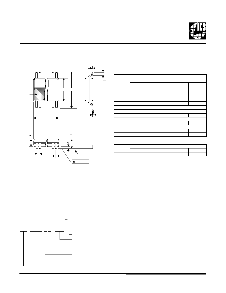
INDEX
AREA
INDEX
AREA
1 2
1 2
N
D
E1
E
SEATING
PLANE
SEATING
PLANE
A1
A
A2
e
- C -
- C -
b
c
L
aaa
C
MIN
MAX
MIN
MAX
A
--
1.20
--
.047
A1
0.05
0.15
.002
.006
A2
0.80
1.05
.032
.041
b
0.13
0.23
.005
.009
c
0.09
0.20
.0035
.008
D
E
E1
4.30
4.50
.169
.177
e
L
0.45
0.75
.018
.030
N
0∞
8∞
0∞
8∞
aaa
--
0.08
--
.003
VARIATIONS
MIN
MAX
MIN
MAX
48
9.60
9.80
.378
.386
10-0037
SYMBOL
In Millimeters
In Inches
COMMON DIMENSIONS COMMON DIMENSIONS
SEE VARIATIONS
SEE VARIATIONS
6.40 BASIC
0.252 BASIC
0.40 BASIC
0.016 BASIC
SEE VARIATIONS
SEE VARIATIONS
N
D mm.
D (inch)
Reference Doc.: JEDEC Publication 95, MO-153
4.40 mm. Body, 0.40 mm. pitch TSSOP
(173 mil)
(16 mil)
Ordering Information
ICSSSTV16857yL-T
Designation for tape and reel packaging
Pattern Number (2 or 3 digit number for parts with ROM code patterns)
Package Type
L=TSSOP (TVSOP)
Revision Designator (will not correlate with datasheet revision)
Device Type (consists of 3 or 4 digit numbers)
Prefix
ICS, AV = Standard Device
Example:
ICS XXXX y L - PPP - T
ICS reserves the right to make changes in the device data identified in
this publication without further notice. ICS advises its customers to
obtain the latest version of all device data to verify that any
information being relied upon by the customer is current and accurate.