Äîêóìåíòàöèÿ è îïèñàíèÿ www.docs.chipfind.ru
Integrated
Circuit
Systems, Inc.
ICSSSTV16859
0003G--05/21/02
Recommended Applications:
· DDR Memory Modules
· Provides complete DDR DIMM logic solution with
ICS93V857 or ICS95V857
· SSTL_2 compatible data registers
Product Features:
· Differential clock signals
· Meets SSTL_2 signal data
· Supports SSTL_2 class II specifications on outputs
· Low-voltage operation
- V
DD
= 2.3V to 2.7V
· Available in 64 pin TSSOP and 56 pin VFQFN (MLF2)
packages
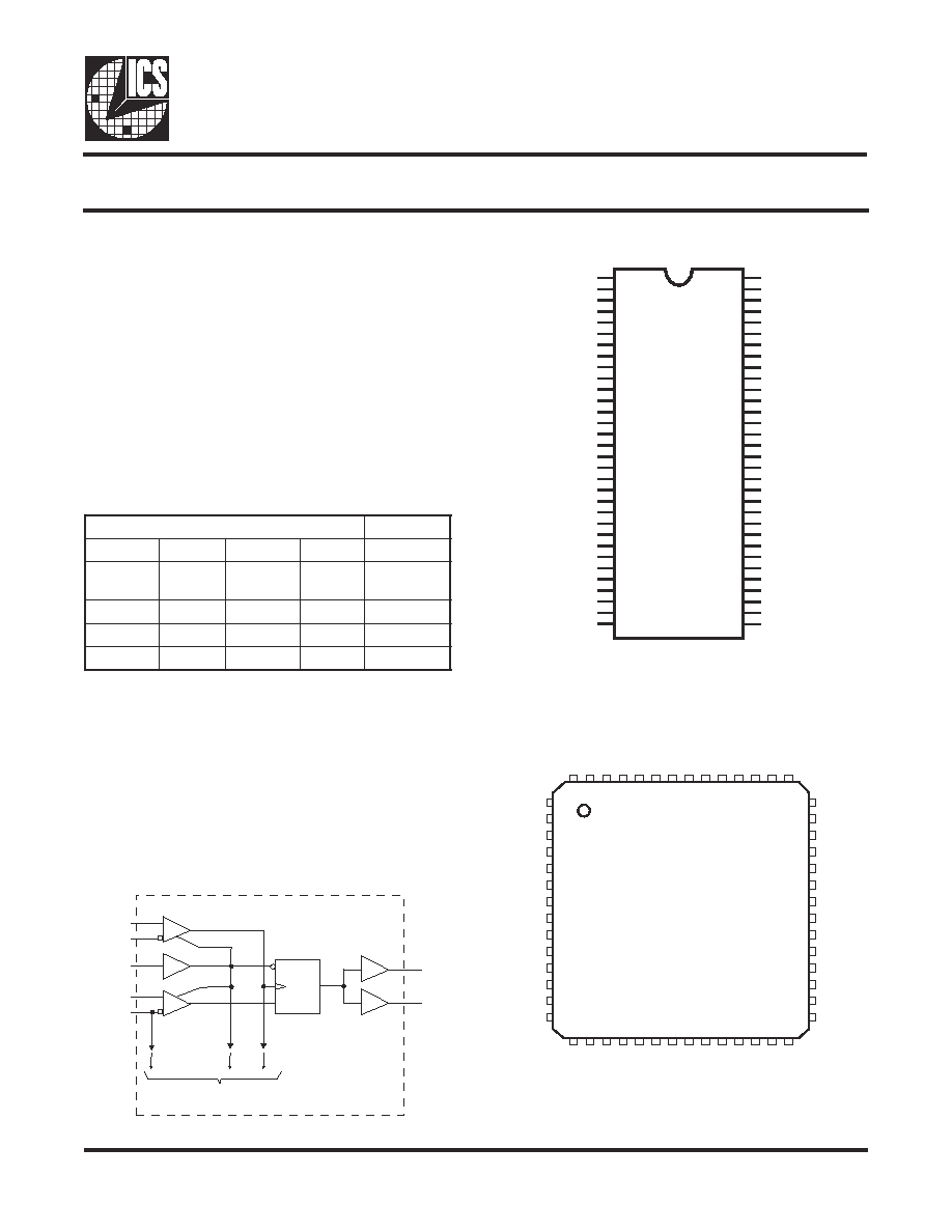
DDR 13-Bit to 26-Bit Registered Buffer
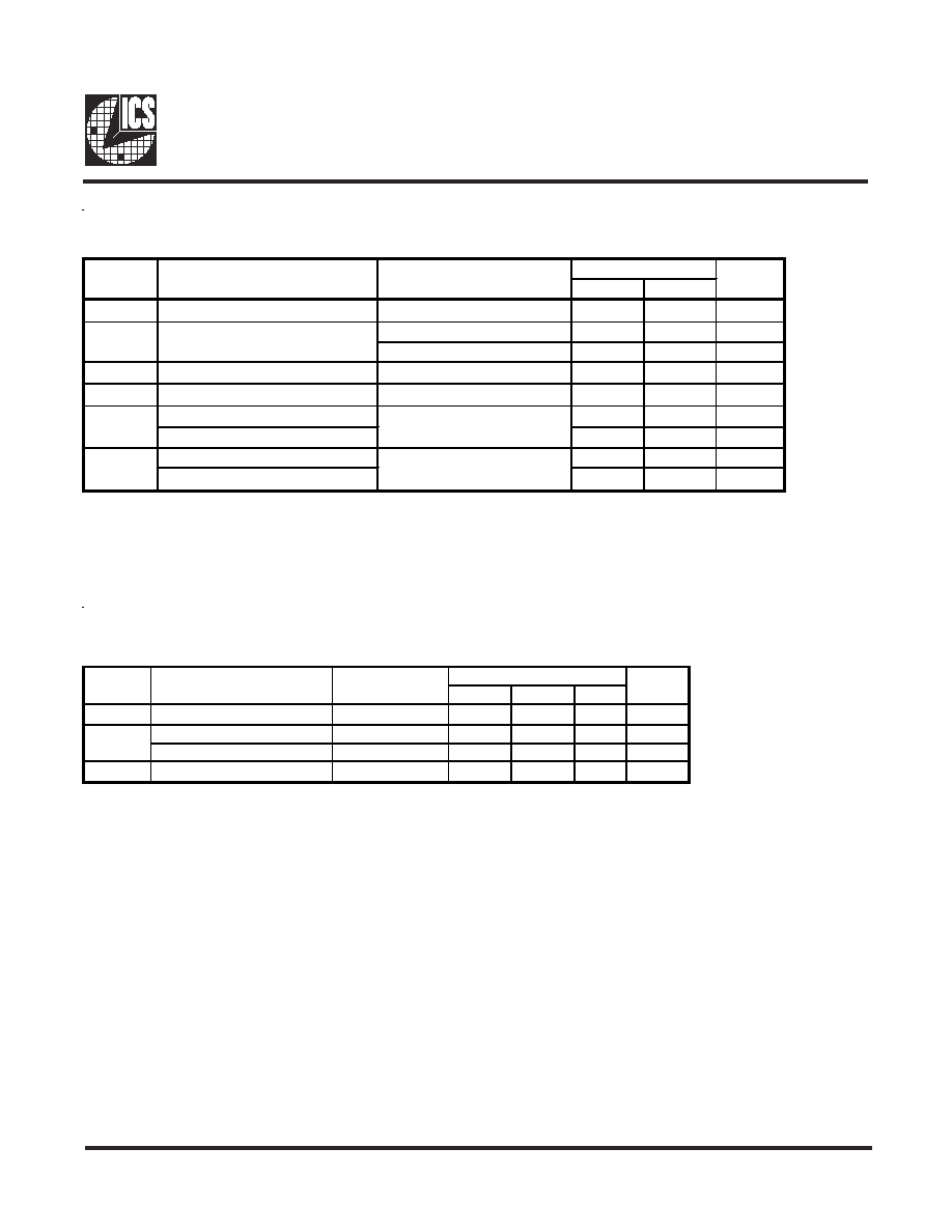
Truth Table
1
Block Diagram
Notes:
1.
H = "High" Signal Level
L = "Low" Signal Level
= Transition "Low"-to-"High"
= Transition "High"-to-"Low"
X = Don't Care
2.
Output level before the indicated steady state
input conditions were established.
s
t
u
p
n
I
s
t
u
p
t
u
O
Q
#
T
E
S
E
R
K
L
C
#
K
L
C
D
Q
L
r
o
X
g
n
i
t
a
o
l
F
r
o
X
g
n
i
t
a
o
l
F
r
o
X
g
n
i
t
a
o
l
F
L
H
-
¯
H
H
H
-
¯
L
L
H
H
r
o
L
H
r
o
L
X
Q
0
)
2
(
56 pin VFQFN (MLF2)
Pin Configurations
64-Pin TSSOP
1
2
3
4
5
6
7
8
9
10
11
12
13
14
15
16
17
18
19
20
21
22
23
24
25
26
27
28
29
30
31
32
64
63
62
61
60
59
58
57
56
55
54
53
52
51
50
49
48
47
46
45
44
43
42
41
40
39
38
37
36
35
34
33
Q13A
Q12A
Q11A
Q10A
Q9A
VDDQ
GND
Q8A
Q7A
Q6A
Q5A
Q4A
Q3A
Q2A
GND
Q1A
Q13B
VDDQ
Q12B
Q11B
Q10B
Q9B
Q8B
Q7B
Q6B
GND
VDDQ
Q5B
Q4B
Q3B
Q2B
Q1B
VDDQ
GND
D13
D12
VDD
VDDQ
GND
D11
D10
D9
GND
D8
D7
RESET#
GND
CLK#
CLK
VDDQ
VDD
VREF
D6
GND
D5
D4
D3
GND
VDDQ
VDD
D2
D1
GND
VDDQ
ICSSSTV16859
6.10 mm. Body, 0.50 mm. pitch
Q7A
Q6A
Q5A
Q4A
Q3A
Q2A
Q1A
Q13B
VDDQ
Q12B
Q11B
Q10B
Q9B
Q8B
1
14
15
28
29
43
42
56
D10
D9
D8
D7
RESET#
GND
CLK#
CLK
VDDQ
VDD
VREF
D6
D5
D4
Q8A
VDDQ
Q9A
Q10A
Q11A
Q12A
Q13A
VDDQ
GND
D13
D12
VDD
VDDQ
D11
Q7B
Q6B
VDDQ
Q5B
Q4B
Q3B
Q2B
Q1B
VDDQ
D1
D2
VDD
VDDQ
D3
ICSSSTV16859
CLK
CLK#
D1
VREF
RESET#
To 12 Other Channels
Q1A
Q1B
CLK
R
D1
2
ICSSSTV16859
0003G--05/21/02
General Description
Pin Configuration (64-Pin TSSOP)
The 13-bit-to-26-bit ICSSSTV16859 is a universal bus driver designed for 2.3V to 2.7V V
DD
operation and
SSTL_2 I/O levels, except for the LVCMOS RESET# input.
Data flow from D to Q is controlled by the differential clock (CLK/CLK#) and a control signal (RESET#). The
positive edge of CLK is used to trigger the data flow whereas CLK# is used to maintain sufficient noise margins
where as RESET#, an LVCMOS asynchronous signal, is intended for use at the time of power-up only.
ICSSSTV16859 supports low-power standby operation. A logic level "Low" at RESET# assures that all internal
registers and outputs (Q) are reset to the logic "Low" state, and all input receivers, data (D) and clock (CLK/
CLK#) are switched off. Please note that RESET# must always be supported with LVCMOS levels at a valid
logic state because VREF may not be stable during power-up.
To ensure that outputs are at a defined logic state before a stable clock has been supplied, RESET# must be
held at a logic "low" level during power up.
In the DDR DIMM application, RESET# is specified to be completely asynchronous with respect to CLK and
CLK#. Therefore, no timing relationship can be guaranteed between the two signals. When entering a low-power
standby state, the register will be cleared and the outputs will be driven to a logic "Low" level quickly relative
to the time to disable the differential input receivers. This ensures there are no glitches on the output. However,
when coming out of low-power standby state, the register will become active quickly relative to the time to
enable the differential input receivers. When the data inputs are at a logic level "low" and the clock is stable
during the "Low"-to-"High" transition of RESET# until the input receivers are fully enabled, the design ensures
that the outputs will remain at a logic "Low" level.
R
E
B
M
U
N
N
I
P
E
M
A
N
N
I
P
E
P
Y
T
N
O
I
T
P
I
R
C
S
E
D
2
3
-
8
2
,
5
2
-
9
1
,
7
1
,
6
1
,
4
1
-
8
,
5
-
1
)
1
:
3
1
(
Q
T
U
P
T
U
O
t
u
p
t
u
o
a
t
a
D
,
4
5
,
0
5
,
3
4
,
9
3
,
4
3
,
6
2
,
5
1
,
7
3
6
,
8
5
D
N
G
R
W
P
d
n
u
o
r
G
4
6
,
9
5
,
7
4
,
8
3
,
3
3
,
7
2
,
8
1
,
6
Q
D
D
V
R
W
P
l
a
n
i
m
o
n
V
5
.
2
,
e
g
a
t
l
o
v
y
l
p
p
u
s
t
u
p
t
u
O
-
5
5
,
3
5
,
2
5
,
4
4
,
2
4
-
0
4
,
6
3
,
5
3
2
6
,
1
6
,
7
5
)
1
:
3
1
(
D
T
U
P
N
I
t
u
p
n
i
a
t
a
D
8
4
K
L
C
T
U
P
N
I
t
u
p
n
i
k
c
o
l
c
r
e
t
s
a
m
e
v
i
t
i
s
o
P
9
4
#
K
L
C
T
U
P
N
I
t
u
p
n
i
k
c
o
l
c
r
e
t
s
a
m
e
v
i
t
a
g
e
N
0
6
,
6
4
,
7
3
D
D
V
R
W
P
l
a
n
i
m
o
n
V
5
.
2
,
e
g
a
t
l
o
v
y
l
p
p
u
s
e
r
o
C
1
5
#
T
E
S
E
R
T
U
P
N
I
)
w
o
l
e
v
i
t
c
a
(
t
e
s
e
R
5
4
F
E
R
V
T
U
P
N
I
l
a
n
i
m
o
n
V
5
.
2
,
e
g
a
t
l
o
v
e
c
n
e
r
e
f
e
r
t
u
p
n
I
R
E
B
M
U
N
N
I
P
E
M
A
N
N
I
P
E
P
Y
T
N
O
I
T
P
I
R
C
S
E
D
6
5
,
4
5
-
0
5
,
2
2
-
8
1
,
6
1
-
0
1
,
8
-
1
)
1
:
3
1
(
Q
T
U
P
T
U
O
t
u
p
t
u
o
a
t
a
D
8
4
,
7
3
D
N
G
R
W
P
d
n
u
o
r
G
5
5
,
9
4
,
4
4
,
4
3
,
7
2
,
3
2
,
7
1
,
9
Q
D
D
V
R
W
P
l
a
n
i
m
o
n
V
5
.
2
,
e
g
a
t
l
o
v
y
l
p
p
u
s
t
u
p
t
u
O
7
4
,
6
4
,
3
4
-
9
3
,
1
3
-
8
2
,
5
2
,
4
2
)
1
:
3
1
(
D
T
U
P
N
I
t
u
p
n
i
a
t
a
D
5
3
K
L
C
T
U
P
N
I
t
u
p
n
i
k
c
o
l
c
r
e
t
s
a
m
e
v
i
t
i
s
o
P
6
3
#
K
L
C
T
U
P
N
I
t
u
p
n
i
k
c
o
l
c
r
e
t
s
a
m
e
v
i
t
a
g
e
N
5
4
,
3
3
,
6
2
D
D
V
R
W
P
l
a
n
i
m
o
n
V
5
.
2
,
e
g
a
t
l
o
v
y
l
p
p
u
s
e
r
o
C
8
3
#
T
E
S
E
R
T
U
P
N
I
)
w
o
l
e
v
i
t
c
a
(
t
e
s
e
R
2
3
F
E
R
V
T
U
P
N
I
l
a
n
i
m
o
n
V
5
.
2
,
e
g
a
t
l
o
v
e
c
n
e
r
e
f
e
r
t
u
p
n
I
-
D
A
P
r
e
t
n
e
C
R
W
P
)
y
l
n
o
e
g
a
k
c
a
p
2
F
L
M
(
d
n
u
o
r
G
Pin Configuration (56-Pin MLF2)
3
ICSSSTV16859
0003G--05/21/02
Absolute Maximum Ratings
Storage Temperature . . . . . . . . . . . . . . . . . . . . 65°C to +150°C
Supply Voltage . . . . . . . . . . . . . . . . . . . . . . . . . -0.5 to 3.6V
Input Voltage
1
. . . . . . . . . . . . . . . . . . . . . . . . . . . . . . . . .
-0.5 to V
DD
+0.5
Output Voltage
1,2
. . . . . . . . . . . . . . . . . . . . . . . . . . . . .
-0.5 to V
DDQ
+0.5
Input Clamp Current . . . . . . . . . . . . . . . . . . . . ±50 mA
Output Clamp Current . . . . . . . . . . . . . . . . . . . ±50 mA
Continuous Output Current . . . . . . . . . . . . . . . ±50 mA
V
DD
, V
DDQ
or GND Current/Pin . . . . . . . . . . . ±100 mA
Package Thermal Impedance
3
. . . . . . . . . . . . . . .
55°C/W
Stresses above those listed under
Absolute Maximum Ratings may cause permanent damage to the device. These
ratings are stress specifications only and functional operation of the device at these or any other conditions above those
listed in the operational sections of the specifications is not implied. Exposure to absolute maximum rating conditions
for extended periods may affect product reliability.
Notes:
1. The input and output negative voltage
ratings may be excluded if the input
and output clamp ratings are observed.
2. This current will flow only when the
output is in the high state level
V
0
>V
DDQ
.
3. The package thermal impedance is
calculated in accordance with
JESD 51.
Recommended Operating Conditions
PARAMETER
MIN
TYP
MAX
UNITS
V
DD
2.3
2.5
2.7
V
DDQ
2.3
2.5
2.7
V
REF
1.15
1.25
1.35
V
TT
V
REF
- 0.04
V
REF
V
REF
+ 0.04
V
I
Input Voltage
0
V
DDQ
V
IH (DC)
DC Input High Voltage
V
REF
+ 0.15
V
IH (AC)
AC Input High Voltage
V
REF
+ 0.31
V
IL (DC)
DC Input Low Voltage
V
REF
- 0.15
V
IL
(DC)
AC Input Low Voltage
V
REF
- 0.31
V
IH
Input High Voltage Level
1.7
V
IL
Input Low Voltage Level
0.7
V
ICR
Common mode Input Range
0.97
1.53
V
ID
Differential Input Voltage
0.36
V
IX
(V
DDQ
/2) - 0.2
(V
DDQ
/2) + 0.2
I
OH
-20
I
OL
20
T
A
0
70
°C
1
Guarenteed by design, not 100% tested in production.
Operating Free-Air Temperature
RESET#
CLK, CLK#
V
Termination Voltage
Cross Point Voltage of Differential Clock
Pair
High-Level Output Current
Low-Level Output Current
Data Inputs
mA
DESCRIPTION
Supply Voltage
I/O Supply Voltage
Reference Voltage
4
ICSSSTV16859
0003G--05/21/02
Electrical Characteristics - DC
T
A
= 0 - 70º C; V
DD
= 2.5 +/-0.2V, V
DDQ
=2.5 +/-0.2V; (unless otherwise stated)
SYMBOL
PARAMETERS
V
DDQ
MIN
TYP
MAX
UNITS
V
IK
I
I
= -18mA
2.3V
-1.2
I
OH
= -100µA
2.3V-2.7V
V
DDQ
-
0.2
I
OH
= -16mA
2.3V
1.95
I
OL
= 100µA
2.3V-2.7V
0.2
I
OL
= 16mA
2.3V
0.35
I
I
All Inputs
V
I
= V
DD
or GND
2.7V
±5
µA
Standby (Static)
RESET# = GND
0.01
µA
Operating (Static)
V
I
= V
IH(AC)
or V
IL(AC)
,
RESET# = V
DD
50
mA
Dynamic operating
(clock only)
RESET# = V
DD
,
V
I
= V
IH(AC)
or V
IL(AC)
,
CLK and CLK# switching
50% duty cycle.
70
µ/clock
MHz
Dynamic Operating
(per each data input)
RESET# = V
DD
,
V
I
= V
IH(AC)
or V
IL (AC)
,
CLK and CLK# switching
50% duty cycle. One data
input switching at half
clock frequency, 50%
duty cycle
30
µA/ clock
MHz/data
r
OH
Output High
2.3V-2.7V
7
13.5
20
r
OL
Output Low
2.3V-2.7V
7
13
20
r
O(D)
[r
OH
-
r
OL
] each
separate bit
2.5V
4
Data Inputs
2.5
3.5
CLK and CLK#
2.5
3.5
Notes:
1 - Guaranteed by design, not 100% tested in production.
I
O
= 0
CONDITIONS
2.7V
2.5V
V
I
= V
REF
±350mV
V
ICR
= 1.25V, V
I(PP)
= 360mV
pF
I
OH
= -20mA
V
C
i
I
OL
= 20mA
I
O
= 20mA, T
A
= 25° C
V
OH
V
OL
I
DD
I
DDD
5
ICSSSTV16859
0003G--05/21/02
Switching Characteristics
(over recommended operating free-air temperature range, unless otherwise noted) (see Figure 1)
MIN
TYP
MAX
f
max
200
MHz
CLK, CLK# (TSSOP)
Q
1.7
2.3
2.7
ns
CLK, CLK# (VFQFN[MLF2])
Q
1.6
2.1
2.6
ns
t
phl
RESET#
Q
5
ns
SYMBOL
V
DD
= 2.5V ±0.2V
UNITS
From
(Input)
To
(Output)
t
PD
Timing Requirements
1
(over recommended operating free-air temperature range, unless otherwise noted)
MIN
MAX
f
clock
Clock frequency
200
MHz
TSSOP
1.7
2.7
ns
VFQFN (MLF2)
1.6
2.6
ns
t
RST
Reset to output time
5
ns
t
SL
Output slew rate
1
4
V/ns
Setup time, fast slew rate
2 & 4
0.60
ns
Setup time, slow slew rate
3 & 4
0.80
ns
Hold time, fast slew rate
2 & 4
0.40
ns
Hold time, slow slew rate
3 & 4
0.50
ns
1 - Guaranteed by design, not 100% tested in production.
2 - For data signal input slew rate of
1V/ns.
4 - CLK, CLK# signals input slew rate of
1V/ns.
SYMBOL
t
S
T
h
Notes:
t
PD
3 - For data signal input slew rate of
0.5V/ns and < 1V/ns.
V
DDQ
= 2.5V ± 0.2V
UNITS
PARAMETERS
Data before CLK
, CLK#
Data after CLK
, CLK#
Clock to output time