
M2006-12 Datasheet Rev 0.6
Revised 10Mar2003
I n t e g r a t e d C i r c u i t S y s t e m s , I n c .
C o m m u n i c a t i o n s M o d u l e s
w w w. i c s t . c o m
t e l ( 5 0 8 ) 8 5 2 - 5 4 0 0
M2006-12
VCSO B
ASED
FEC C
LOCK
PLL
WITH
APS
Integrated
Circuit
Systems, Inc.
P r e l i m i n a r y I n f o r m a t i o n
G
ENERAL
D
ESCRIPTION
The M2006-12 is a VCSO (Voltage Controlled SAW
Oscillator) based clock generator
PLL designed for clock frequency
translation and jitter attenuation.
The device supports both forward
and inverse FEC (Forward Error
Correction) clock multiplication
ratios. Multiplication ratios are
pin-selected from pre-programming look-up tables.
F
EATURES
Similar to the
M2006-02
(and pin-compatible), but with
an automatic protection switch (APS) function
APS engages when a 4 ns or greater clock phase
change is detected at the phase detector, such as
might occur when reselecting reference clocks
APS helps to ensure MTIE compliance by lowering loop
bandwidth during the phase realignment
APS is not recommended for complex FEC ratio trans-
lation when using an unstable reference; the M2006-02
is recommended for these applications
In addition to the APS circuit, the APC (automatic
phase compensation) pin enables absorption of the
input phase change.
Supports input reference and VCSO frequencies up to
700MHz, supports loop timing modes
Single 3.3V power supply
Small 9 x 9 mm SMT (surface mount) package
P
IN
A
SSIGNMENT
(9 x 9 mm SMT)
Figure 1: Pin Assignment
S
IMPLIFIED
B
LOCK
D
IAGRAM
Figure 2: Simplified Block Diagram
Example I/O Clock Frequency Combinations
Using
M2006-12-622.0800 and
Inverse FEC Ratios
FEC PLL Ratio
Mfec / Rfec
Base Input Rate
1
(MHz)
Note 1: Input reference clock can be the base frequency shown
divided by "Mfin" (as shown in Table 3 on
pg. 3
).
Output Clock
(either output)
MHz
1/1
622.0800
622.08
or
155.52
239/255
663.7255
238/255
666.5143
237/255
669.3266
236/255
672.1627
Table 1: Example I/O Clock Frequency Combinations
M 2 0 0 6 - 1 2
( T o p V i e w )
18
17
16
15
14
13
12
11
10
28
29
30
31
32
33
34
35
36
1
2
3
4
5
6
7
8
9
F
I
N
_
SEL
1
GN
D
AP
C
DI
F
_RE
F
0
n
D
I
F
_RE
F
0
RE
F
_
S
E
L
DI
F
_RE
F
1
n
D
I
F
_RE
F
1
VC
C
P0_SEL
P1_SEL
nFOUT0
FOUT0
GND
nFOUT1
FOUT1
VCC
GND
FIN_SEL0
FEC_SEL0
FEC_SEL1
FEC_SEL2
FEC_SEL3
VCC
DNC
DNC
DNC
nOP
_
I
N
O
P
_O
UT
VC
nV
C
nOP
_
OU
T
OP
_
I
N
GN
D
GN
D
GN
D
19
20
21
22
23
24
25
26
27
Rfec Div
VCSO
P0 Div
Mfin Div
Mfec Div
Mfec / Rfec
Divider LUT
Mfin Divider
LUT
FIN_SEL1:0
REF_SEL
DIF_REF0
nDIF_REF0
DIF_REF1
nDIF_REF1
P0_SEL
P1 Div
P1_SEL
0
1
M2006-12
FOUT0
nFOUT0
FOUT1
nFOUT1
FEC_SEL3:0
4
2
APC
M2006-12 VCSO Based FEC Clock PLL with APS

M2006-12 Datasheet Rev 0.6
2 of 8
Revised 10Mar2003
I n t e g r a t e d C i r c u i t S y s t e m s , I n c .
C o m m u n i c a t i o n s M o d u l e s
w w w. i c s t . c o m
t e l ( 5 0 8 ) 8 5 2 - 5 4 0 0
Integrated
Circuit
Systems, Inc.
M2006-12
VCSO B
ASED
FEC C
LOCK
PLL
WITH
APS
P r e l i m i n a r y I n f o r m a t i o n
D
ETAILED
B
LOCK
D
IAGRAM
Figure 3: Detailed Block Diagram
P
IN
D
ESCRIPTIONS
Number
Name
I/O
Configuration
Description
1, 2, 3, 10, 14, 26 GND
Ground
Power supply ground connections.
4
9
OP_IN
nOP_IN
Input
External loop filter connections. See
Figure 4
.
5
8
nOP_OUT
OP_OUT
Output
6
7
nVC
VC
Input
11, 19, 33
VCC
Power
Power supply connection, connect to +
3.3
V.
12, 13
FOUT1, nFOUT1
Output
No internal terminator
Clock output pairs. Differential LVPECL.
15, 16
FOUT0, nFOUT0
17
18
P1_SEL
P0_SEL
Input
Internal pull-down
resistor
1
P Divider controls. LVCMOS/LVTTL.
(For
P0_SEL, P1_SEL
, see
Table 5
on
pg. 3
.
20
21
nDIF_REF1
DIF_REF1
Input
Internal pull-down
resistor
1
Note 1: For typical values of internal pull-down and pull-up resistors, see
DC Characteristics
(
Pull-down
and
Pull-up
) on
pg. 7
.
Reference clock input pair 1.
Differential LVPECL or LVDS.
22
REF_SEL
Input
Internal pull-down
resistor
1
Reference clock input selection. LVCMOS/LVTTL:
Logic
1
selects
DIF_REF1, nDIF_REF1.
Logic
0
selects
DIF_REF0, nDIF_REF0
.
23
24
nDIF_REF0
DIF_REF0
Input
Internal pull-down
resistor
1
Reference clock input pair 0.
Differential LVPECL or LVDS.
25
APC
Input
Internal pull-down
resistor
1
Automatic Phase Compensation.
LVCMOS/LVTTL:
Logic
1
- Device absorbs input phase transients
.
Logic
0
- Device doesn't absorb transients.
27
28
FIN_SEL1
FIN_SEL0
Input
Internal pull-down
resistor
1
I
nput clock frequency selection. LVCMOS/LVTTL.
(For
FIN_SEL1:0
, see
Table 3
on
pg. 3
.
29
30
31
32
FEC_SEL0
FEC_SEL1
FEC_SEL2
FEC_SEL3
Input
Internal pull-up resistor
1
FEC PLL divider ratio selection. LVCMOS/ LVTTL.
(For
FEC_SEL3:0
, see
Table 4
on
pg. 3
.)
34, 35, 36
DNC
Do Not Connect.
Table 2: Pin Descriptions
Phase
Locked
Loop
(PLL)
M2006-12
SAW Delay Line
Phase
Shifter
VCSO
C
POST
C
POST
VC
nVC
R
POST
nOP_OUT
OP_OUT
R
POST
R
LOOP
R
LOOP
C
LOOP
C
LOOP
R
IN
R
IN
OP_IN
nOP_IN
Phase
Detector
Loop Filter
Amplifier
External
Loop Filter
Components
FOUT0
nFOUT0
FEC_SEL3:0
P0_SEL
FIN_SEL1:0
Rfec
Divider
MUX
0
REF_SEL
APC
DIF_REF1
nDIF_REF1
DIF_REF0
nDIF_REF0
1
FOUT1
nFOUT1
P1_SEL
2
Mfec / Rfec
Divider LUT
4
Mfin Divider
LUT
Mfin Divider
Mfec Divider
P1 Divider
P = 1 ( P1_SEL = 0 )
or 4 ( P1_SEL = 1 )
P0 Divider
P = 1 ( P0_SEL = 0 )
or 4 ( P0_SEL = 1 )

M2006-12 Datasheet Rev 0.6
3 of 8
Revised 10Mar2003
I n t e g r a t e d C i r c u i t S y s t e m s , I n c .
C o m m u n i c a t i o n s M o d u l e s
w w w. i c s t . c o m
t e l ( 5 0 8 ) 8 5 2 - 5 4 0 0
M2006-12
VCSO B
ASED
FEC C
LOCK
PLL
WITH
APS
P r e l i m i n a r y I n f o r m a t i o n
Integrated
Circuit
Systems, Inc.
PLL D
IVIDER
L
OOK
-U
P
T
ABLES
Mfin (Frequency Input) Divider Look-Up Table (LUT)
The
FIN_SEL1:0
pins select the feedback divider value
("Mfin").
FEC PLL Ratio Dividers Look-up Table (LUT)
The
FEC_SEL3:0
pins select the FEC feedback and
reference divider values Mfec and Rfec.
Post-PLL Dividers
The M2006-12 also features two post-PLL dividers,
one for each output pair. The "P1" divider is for
FOUT1
and
nFOUT1
; the "P0" divider is for
FOUT0
and
nFOUT0
.
Each divides the VCSO frequency to produce one of
two output frequencies (1/4 or 1/1 of the VCSO
frequency). The
P1_SEL
and
P0_SEL
pins each select the
value for their corresponding divider.
F
UNCTIONAL
D
ESCRIPTION
The M2006-12 is a PLL (Phase Locked Loop) based
clock generator that generates output clocks synchro-
nized to one of two selectable input reference clocks.
An internal high "Q" SAW filter provides low jitter signal
performance and controls the output frequency of the
VCSO (Voltage Controlled SAW Oscillator).
Configurable FEC feedback and reference dividers (the
"Mfec Divider" and "Rfec Divider") provide the
multiplication ratios necessary to accomodate clock
translation for both forward and inverse Forward Error
Correction.
In addition, a configurable feedback divider (labeled
"Mfin Divider") provides the broader division options
needed to accomodate various reference clock
frequencies.
For example, the
M2006-12-622.0800
(see
"Ordering
Information"
on
pg. 8
)
has a
622.08
MHz VCSO
frequency:
�
The inverse FEC PLL ratios (at top of Table 4) enable
the
M2006-12-622.0800
to accept "base" input reference
frequencies of:
663.7255
,
666.5143
,
669.3266
,
672.1627
, and
622.08
MHz.
�
The Mfin feedback divider enables the actual input
reference clock to be the "base" input frequency
divided by
1
,
4
,
8
, or
32
. Therefore, for the base input
frequency of
622.08
MHz, the actual input reference
clock frequencies can be:
622.08
,
155.52
,
77.76
, and
19.44
MHz. (See Table 3 on
pg. 3
.)
FIN_SEL1:0
Mfin Value
M2006-12-622.0800
Sample Ref. Freq. (MHz)
1
Note 1: Example with M2006-12-622.0800 and "Non-FEC ratio"
selection made from Table 4 (FEC_SEL2=1).
1
1
1
622.08
2
Note 2: Do not use with FEC_SEL3:0=1100 or 1101.
1
0
4
155.52
0
1
8
77.76
0
0
32
19.44
Table 3: Mfin (Frequency Input) Divider Look-Up Table (LUT)
FEC_SEL3:0
Mfec Rfec
Description
0 0 0 0
236
255
Inverse FEC ratio
0 0 0 1
79
85
Inverse FEC ratio, equivalent to
237/255
0 0 1 0
14
15
Inverse FEC ratio, equivalent to
238/255
0 0 1 1
239
255
Inverse FEC ratio
0 1 0 0
236
236
Non-FEC ratio, complement to
000
1
Note 1: The complementary "Inverse FEC ratio" and "Non-FEC ratio"
selections use the same Mfec Divider ratio. This results in the
same PLL loop bandwidth and damping factor for both
selections, enabling them to be actively switched in a given
application. See
"Maintaining PLL Lock:"
on
pg. 4
.
0 1 0 1
79
79
Non-FEC ratio, complement to
001
1
0 1 1 0
14
14
Non-FEC ratio, complement to
010
1
0 1 1 1
239
239
Non-FEC ratio, complement to
011
1
1 0 0 0
255
236
FEC ratio
1 0 0 1
85
79
FEC ratio, equivalent to 255/237
1 0 1 0
15
14
FEC ratio, equivalent to 255/238
1 0 1 1
255
239
FEC ratio
1 1 0 0
1
1
Non-FEC ratio. Do not use when
FIN_SEL1:0=11.
The maximum phase
detector frequency is
175
MHz
2
Note 2: The various "Non-FEC ratio" settings can be used to actively
change PLL loop bandwidth in a given application.
1 1 0 1
2
2
1 1 1 0
4
4
Non-FEC ratio
2
1 1 1 1
8
8
Table 4: FEC PLL Ratio Dividers Look-up Table (LUT)
P1_SEL, P0_SEL
P Value
M2006-12-622.0800
Output Frequency
(MHz)
1
4
155.52
0
1
622.08
Table 5: P Divider Selector, Values, and Frequencies

M2006-12 Datasheet Rev 0.6
4 of 8
Revised 10Mar2003
I n t e g r a t e d C i r c u i t S y s t e m s , I n c .
C o m m u n i c a t i o n s M o d u l e s
w w w. i c s t . c o m
t e l ( 5 0 8 ) 8 5 2 - 5 4 0 0
Integrated
Circuit
Systems, Inc.
M2006-12
VCSO B
ASED
FEC C
LOCK
PLL
WITH
APS
P r e l i m i n a r y I n f o r m a t i o n
The PLL
The PLL uses a phase detector and configurable
dividers to synchronize the output of the VCSO with
selected reference clock.
The "Mfin Divider" and "Mfec Divider" divide the VCSO
frequency, feeding the result into the phase detector.
The selected input reference clock is divided by the
"Rfec Divider". The result is fed into the other input of
the phase detector.
The phase detector compares its two inputs. It then
outputs pulses to the loop filter as needed to increase or
decrease the VCSO frequency and thereby match and
lock the divider output's frequency and phase to those
of the input reference clock.
Due to the narrow tuning range of the VCSO
(+200ppm), appropriate selection of all of the following
are required for the PLL be able to lock: VCSO center
frequency, input frequency, and divider selections.
See also
"Maintaining PLL Lock:"
on
pg. 4
.
Relationship Among Frequencies and Dividers
The VCSO center frequency must be specified at time
of order. The relationship between the VCSO (Fvcso)
frequency, the Mfin divider, the Mfec divider, the Rfec
divider, and the input reference frequency (Fin) is:
As an example, for the
M2006-12-622.0800
, the first five PLL
ratios in Table 4 enable use with these corresponding
input reference frequencies:
Maintaining PLL Lock:
The narrow tuning range of the VCSO requires that the
input reference frequency must remain suitable for the
current look-up table selection. For example, when
switching between "Inverse FEC ratio" and "Non-FEC
ratio" look-up table selections (see Table 4 on
pg. 3
), the
input reference frequency must change accordingly in
order for the PLL to lock.
An out-of-lock condition due to an inappropriate
configuration will typically result in the VCSO
operating at its lower or upper frequency rail,
which is approximately 200ppm above or below
the nominal VCSO center frequency.
See also
"Automatic Protection Switch (APS)"
(next) for
an additional issue with regard to phase locking.
Automatic Protection Switch (APS)
The M2006-12 includes a proprietary automatic
protection switch (APS) circuit that prevents excessive
phase transients of the output clocks upon input
reference rearrangement. Upon the occurance of an
input reference phase change, or phase transient, PLL
bandwidth is lowered by the APS circuit. This limits the
rate of phase change in the output clocks. With proper
configuration of the external loop filter, the output clocks
will comply with MTIE (maximum time interval error)
specifications for GR-253 (SONET) and ITU G.813
(SDH) during input reference clock changes.
The APS circuit uses a phase error detector at the
phase detector to detect a clock phase change. During
normal operation with a stable reference clock, the PLL
will be frequency locked and phase locked, resulting in
very little error at the phase detector (<1 ns). Upon the
selection of a new input reference clock at a different
clock phase, a phase error will occur at the phase
detector. The APS circuit is triggered with a phase error
greater than 4 ns, upon which a narrow PLL bandwidth
is applied. When the PLL locks to within 2 ns error at the
phase detector, wide bandwidth (normal) operation is
resumed.
The APS circuit is not suitable for situations in which an
unstable reference is used. Under normal conditions
the reference clock jitter should not induce phase jitter
at the phase detector beyond 2 ns. (This includes when
subjecting the system to jitter tolerance compliance
testing.) Because of this, the M2006-12 is not
recommended for use with some Stratum DPLL clock
sources, or with unstable recovered network clocks
intended for loop timing configuration. It is also not
recommended for complex FEC ratios where the phase
detector is operated at less 1 MHz. For these
applications the
M2006-02
is suggested. The M2006-02
is identical to the M2006-12 except that it does not
include the APS function or the APC function discussed
in the following section.
M2006-12-622.0800
M2006-12-622.0800
VCSO Clock
Frequency (MHz)
FEC Ratio
=
Base Input Ref.
Frequency (MHz)
1
Note 1: Input reference clock ("Fin") can be the base frequency
shown divided by "Mfin" (as shown in Table 3 on
pg. 3
).
622.08
1
/
1
622.0800
239
/ 255
663.7255
238
/ 255
666.5143
237
/ 255
669.3266
236
/ 255
672.1627
Table 6: Example FEC PLL Rations and Input Reference Frequencies
Fvcso
Fin Mfin
�
Mfec
Rfec
--------------
�
=
�
M2006-12 Datasheet Rev 0.6
5 of 8
Revised 10Mar2003
I n t e g r a t e d C i r c u i t S y s t e m s , I n c .
C o m m u n i c a t i o n s M o d u l e s
w w w. i c s t . c o m
t e l ( 5 0 8 ) 8 5 2 - 5 4 0 0
M2006-12
VCSO B
ASED
FEC C
LOCK
PLL
WITH
APS
P r e l i m i n a r y I n f o r m a t i o n
Integrated
Circuit
Systems, Inc.
Automatic Phase Compensation (APC) Pin
The M2006-12 also includes an automatic phase
compensation (APC) circuit that can be selectively
enabled by asserting the APC input (pin
25
) to logic
1
.
The APC circuit works in conjunction with the APS
circuit. When asserted, the APC circuit enables the PLL
to absorb most of the phase change of the input clock
which reduces re-lock time and the generation of
wander. (Wander is created in this case by the
generation of extra output clock cycles.)
When asserted, the APC circuit is triggered by same
>4 ns phase transient (at the phase detector) that
triggers the APS circuit. Once triggered, a new VCSO
clock edge is selected for the phase comparator
feedback input. (The clock edge selected is the one
closest in phase to the new input clock phase.) The
residual phase detector phase error following
reselection is approximately 3-to-4 ns. The narrow
bandwidth selected by the APS circuit minimizes VCSO
drifting and switch transients during the process.
It is recommended that APC remain disabled (APC pin
low) when the phase detector frequency is less than
4 MHz. Otherwise, the M2006-12 may have difficulty
locking to reference upon power-up.
Outputs
The M2006-12 provides a total of two differential
LVPECL output pairs:
FOUT1
and
FOUT0.
Because each
output pair has its own P divider, the
FOUT1
pair and the
FOUT_0
can output the two different frequencies at the
same time. For example,
FOUT1
can output
155.52
MHz
while
FOUT0
outputs
622.08
MHz.
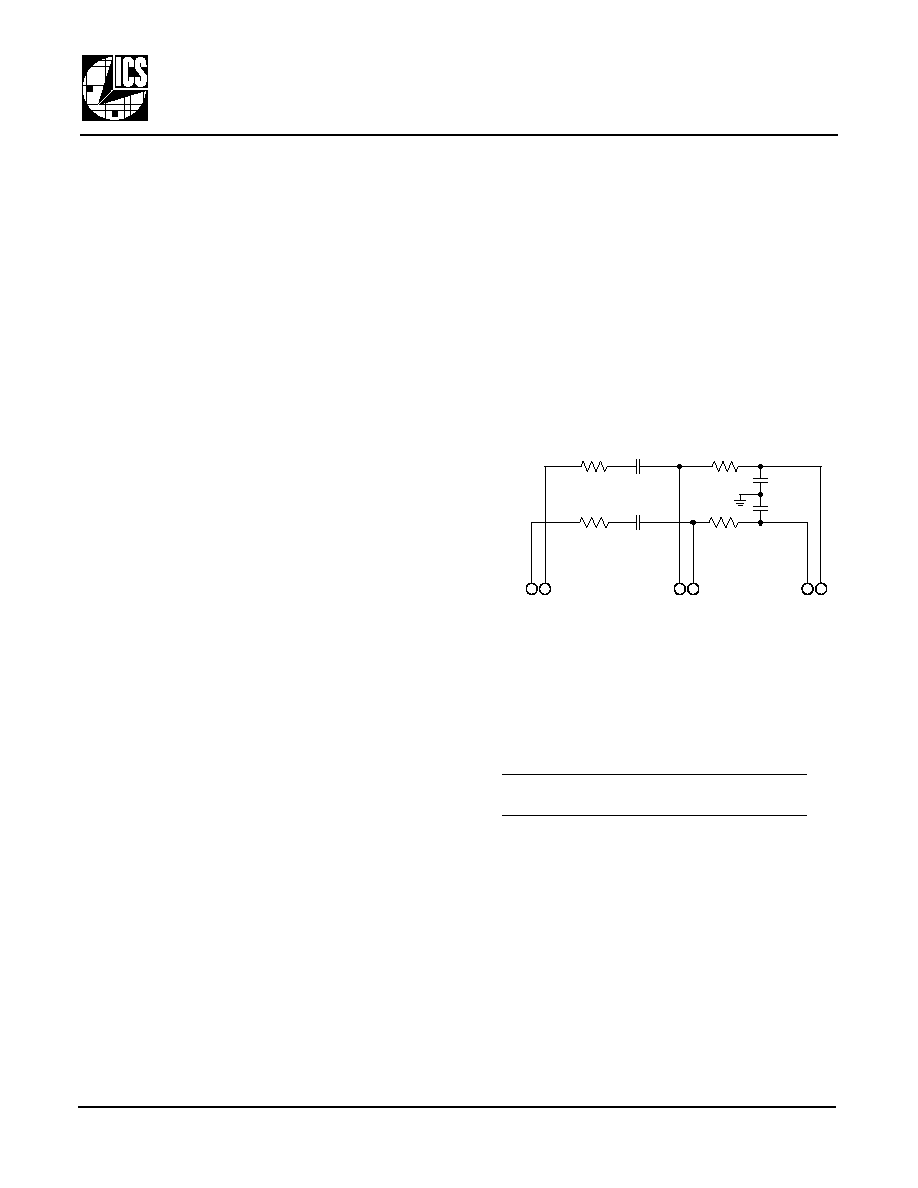
External Loop Filter
To provide stable PLL operation, and thereby a low jitter
output clock, the M2006-12 requires the use of an
external loop filter. This is provided via the provided
filter pins (see
Figure 4
).
Due to the differential signal path design, the
implementation requires two identical complementary
RC filters as shown here.
Figure 4: External Loop Filter
PLL bandwidth is affected by the "Mfec" value and the
"Mfin" value, as well as the VCSO frequency.
The various "Non-FEC ratio" settings can be used to
actively change PLL loop bandwidth in a given
application. See
"FEC PLL Ratio Dividers Look-up
Table (LUT)"
on
pg. 3
.
Consult factory for external loop filter component
values.
C
POST
C
POST
VC
nVC
R
POST
nOP_OUT
OP_OUT
R
POST
R
LOOP
R
LOOP
C
LOOP
C
LOOP
OP_IN
nOP_IN
6
7
5
4
9
8