Micro Networks 324 Clark Street Worcester, MA 01606 tel: 508-852-5400 fax: 508-852-8456 www.micronetworks.com
M2005-02
Preliminary Specifications
1
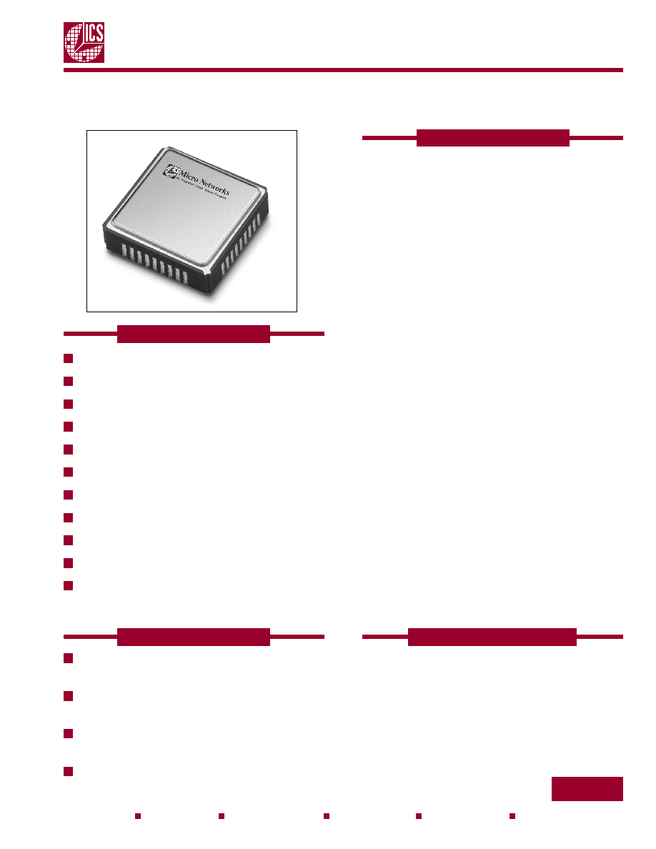
Micro Networks
An Integrated Circuit Systems Company
ISO 9001
Registered
ISO 9001
Registered
M2005-02
Frequency Translator
APPLICATIONS
SONET / SDH / 10GbE System
Synchronization
Add / Drop Muxes, Access and Edge
Switches
Line Card System Clock Cleaner /
Translator
Optical Module Clock Cleaner / Translator
DESCRIPTION
The M2005-02 integrates a high performance Phase
Locked Loop (PLL) with a Voltage Controlled SAW
Oscillator (VCSO) to provide a low jitter Frequency
Synthesizer in a 9mm x 9mm surface mount
package.
The internal high "Q" SAW filter provides low jitter
signal performance and determines the maximum
output frequency of the VCSO. A programmable
output divider can divide the VCSO frequency by a
factor of 4 to achieve an output as low as 77.76MHz
with a 311.04MHz VCSO.
The input to the Frequency Synthesizer is provided
by selecting between one of two input reference
clocks. The maximum input frequency is 250 MHz.
Serial control of the input divider, the feedback
divider, and output divider is provided via the
configuration logic.
An external loop filter sets the PLL bandwidth which
can be optimized to provide jitter attenuation of the
input reference clock.
A HOLD feature freezes the VCSO frequency so that
a stable output clock can be maintained when both
input reference clocks are lost.
The bandwidth control, low phase noise, and HOLD
features make the M2005-02 ideal for use as a clock
jitter attenuator, frequency translator, and clock
frequency generator in OC-3 through OC-192
applications.
Inputs, V
I
:
................................................. -0.5 to V
CC
+0.5V
Output, V
O
:
................................................. -0.5 to V
CC
+0.5V
Supply Voltage, V
CC
: ......................................................... 4.6 V
Storage Temperature, T
STO
: ............................ -45�C to +100�C
Stresses beyond those listed under Absolute Maximum Ratings may cause
permanent damage to the device. These ratings are stress specifications
only. Functional operation of product at these conditions or any conditions
beyond those listed in the DC Characteristics or AC Characteristics is not
implied. Exposure to absolute maximum rating conditions for extended peri-
ods may affect product reliability.
ABSOLUTE MAX RATINGS
Output Clock Frequency up to 700MHz
Differential LVPECL Outputs
Internal Low-jitter SAW-based Oscillator
Intrinsic Jitter <1ps rms (12kHz - 20MHz)
Jitter Attenuation of Input Reference Clock
Dual Input MUX
Configurable Loop and Output Dividers
Tunable Loop Filter Response
Single 3.3V Supply
Small 9mm x 9mm SMT Package
HOLD Mode During Loss of Input
Reference Clock
FEATURES
Micro Networks 324 Clark Street Worcester, MA 01606 tel: 508-852-5400 fax: 508-852-8456 www.micronetworks.com
M2005-02
Preliminary Specifications
2
Micro Networks
An Integrated Circuit Systems Company
M2005-02
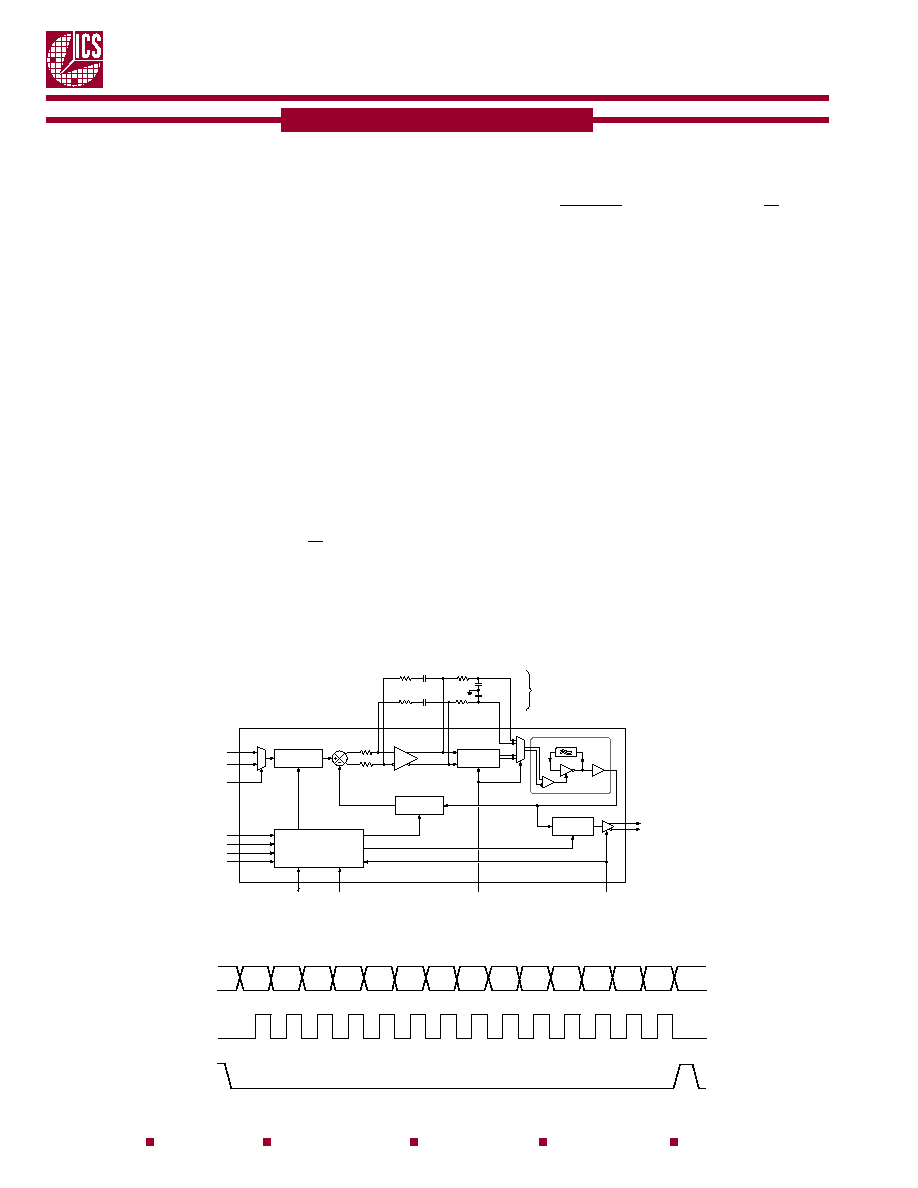
SAW Delay Line
Phase
Shifter
VCSO
VC
nVC
nOP_OUT
OP_OUT
OP_IN
nOP_IN
M Divider
M = 3 to 131,071
P Divider
P = 1 or 4
Serial / Parallel
Configuration Register
6
M5:0
P1
Phase
Detector
Loop Filter
Amplifier
External
Loop Filter
Components
FOUT
nFOUT
Frequency
Hold
MR
0
1
HOLD
S_DATA
S_CLK
S_LOAD
nP_LOAD
R Divider
R=1,2,4 to 511
MUX
0
1
REF_SEL
REF_CLK0
REF_CLK1
RLOOP CLOOP
RPOST
CPOST
CPOST
RLOOP CLOOP
RPOST
RIN
RIN
The internal PLL will adjust the VCSO output
frequency to be M (feedback divider) divided by P
(input divider) times the selected input reference
clock frequency. Note that the ratio of M/P times
input frequency must be such that it falls within the
"lock" range of the VCSO. The M divider (17-bits)
can be programmed for a maximum value of
131,071 and a minimum value of 4. The P divider
(9-bits) can be set to a maximum value of 511 and
a minimum value of 1. The N output divider can be
programmed to divide the VCSO output frequency
by 1, or 4 and provide a 50% output duty cycle.
The M2005-02 is serially programmed via a 3 wire
interface. Figure 1 shows the timing diagram for
serial programming.
The relationship between the VCSO frequency, the
M & P dividers, and the input REF_CLK is defined
as follows:
F VCSO = F REF_CLK x
M
P
When the N output divider is included, the
complete relationship for the output frequency is
defined as:
FOUT = F VCSO = F REF_CLK x
M
N
N x P
The N1 input can be hard wired to set the N divider
to a specific state that will automatically occur
during power-up.
Serial operation occurs when S_LOAD is LOW. The
shift register is loaded by sampling the S_DATA bits
with the rising edge of S_CLOCK. The contents of
the shift register are loaded into the M divider and
N output divider when S_LOAD transitions from
LOW-to-HIGH. The M divider and N output divide
values are latched on the HIGH-to- LOW transition
of S_LOAD. If S_LOAD is held HIGH, data at the
S_DATA input is passed directly to the M divider
and N output divider on each rising edge of
S_CLOCK.
When the HOLD input is asserted the M2005-02
will revert back to the initial accuracy of the VCSO
and remain at that frequency until the HOLD signal
is returned LOW.
FUNCTIONAL BLOCK DIAGRAM
FIGURE 1
Low Low Null
Null Null Null
N1
N0
M5
M4
M3
M2
M1
M0
S_DATA
S_CLK
S_LOAD
Micro Networks 324 Clark Street Worcester, MA 01606 tel: 508-852-5400 fax: 508-852-8456 www.micronetworks.com
M2005-02
Preliminary Specifications
3
Micro Networks
An Integrated Circuit Systems Company
FUNCTIONAL DESCRIPTION
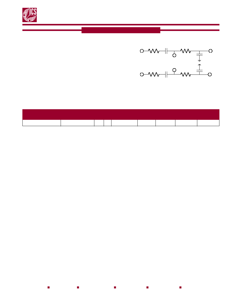
LOOP FILTER
FIGURE 2
TABLE 1. RECOMMENDED LOOP FILTER VALUES
The M2005-02 requires the use of an external loop
filter via the provided filter pins. Due to the
differential design, the implementation requires two
identical RC filters as shown in Figure 2.
REF_CLK
VCSO
M
N
Fout
Rloop
Cloop
Rpost
Cpost
Frequency
Frequency
19.44MHz
622.0800MHz
32
1
622.0800MHz
5K
1MF
50K
100pf
Vc
nVc
OP_OUT
nOP_OUT
OP_IN
nOP_IN
Rloop
Rloop
Cloop
Cloop
Rpost
Rpost
Cpost
Cpost
Micro Networks 324 Clark Street Worcester, MA 01606 tel: 508-852-5400 fax: 508-852-8456 www.micronetworks.com
M2005-02
Preliminary Specifications
4
Micro Networks
An Integrated Circuit Systems Company
PIN DESCRIPTIONS
TABLE 2
Pin Number
Name
I/O
Configuration
Description
1, 2, 3
GND
GND
Power Supply Ground
4, 9
OP_IN, nOP_IN
Analog I/O
Used for external loop filter. See Figure 2.
5, 8
nOP_Out, OP_OUT
Analog I/O
Used for external loop filter. See Figure 2.
6, 7
nVC, VC
Input
VCSO Differential Control Voltage Input Pair
10, 14, 26
GND
GND
Power Supply Ground
11, 19, 22, 33
VCC
Power
Positive Supply Pins
12
HOLD
Input
Pull - down
When HIGH the device operates in digital HOLD
mode. LVCMOS / LVTTL interface levels.
13
N1
Input
Pull - down
Determines the output divider value as
defined in Table 3C. LVCMOS / LVTTL
interface levels.
15, 16
FOUT, nFOUT
Output
Unterminated
Differential output, 3.3V LVPECL levels.
17
MR
Input
Pull - down
Logic HIGH resets the reference frequency and N
output dividers. Logic LOW enables the outputs.
LVCMOS / LVTTL interface levels.
18
S_CLOCK
Input
Pull - down
Clocks in serial data present at S_DATA input
into the shift register on the rising edge of
S_CLOCK.
20
S_DATA
Input
Pull - down
Shift register serial input. Data is sampled on the
rising edge of S_CLOCK.
21
S_LOAD
Input
Pull - down
Controls transition of data from shift register into
the dividers. LVCMOS / LVTTL interface levels
23
REF_CLK1
Input
Pull - down
Input reference clock. LVCMOS / LVTTL interface
levels.
24
REF_CLK0
Input
Pull - down
Input reference clock. LVCMOS / LVTTL interface
levels.
25
REF_SEL
Input
Pull - down
Selects between the different reference clock
inputs as the PLL reference source. See Table
3D. LVCMOS / LVTTL interface levels.
27, 28, 29, 30, 31
N/C
No connection. Internal test pins.
32, 34, 35, 36
Micro Networks 324 Clark Street Worcester, MA 01606 tel: 508-852-5400 fax: 508-852-8456 www.micronetworks.com
M2005-02
Preliminary Specifications
5
Micro Networks
An Integrated Circuit Systems Company
TABLE 4
PARALLEL & SERIAL MODES FUNCTION
PIN CHARACTERISTICS
Symbol
Parameter
Test Conditions
Min
Typical
Max
Units
C
IN
Input Capacitance
4
pF
R
PULLUP
Input Pullup Resistor
51
k
R
PULLDOWN
Input Pulldown Resistor
51
k
TABLE 5A
Inputs
MR
nP_LOAD
M
N
S_LOAD
S_CLOCK
S_DATA
Conditions
H
X
X
X
X
X
X
Reset, Forces outputs LOW.
L
H
X
X
L
Data
Serial input mode. Shift register is loaded with data
on S_DATA on each rising edge of S_CLOCK.
L
H
X
X
L
Data
Contents of the shift register are passed to the M
divider and N output divider.
L
H
X
X
L
Data
M divider and N output divider values are latched.
L
H
X
X
L
X
X
Parallel or serial input do not affect shift registers.
L
H
X
X
H
Data
S_DATA passed directly to M divider as it is
clocked.
Note: L = Low; H = High; X = Don't care; = Rising Edge Transition; = Falling Edge Transition