DATA SHEET
Product specification
File under Integrated Circuits, IC12
1997 Feb 13
INTEGRATED CIRCUITS
PCF85xxC-2 family
256 to 1024
◊
8-bit CMOS
EEPROMs with I
2
C-bus interface

1997 Feb 13
2
Philips Semiconductors
Product specification
256 to 1024
◊
8-bit CMOS EEPROMs with
I
2
C-bus interface
PCF85xxC-2 family
CONTENTS
1
FEATURES
2
GENERAL DESCRIPTION
3
QUICK REFERENCE DATA
4
ORDERING INFORMATION
5
DEVICE SELECTION
6
BLOCK DIAGRAM
7
PINNING
7.1
Pin description PCF8582C-2
7.2
Pin description PCF8594C-2
7.3
Pin description PCF8598C-2
8
I
2
C-BUS PROTOCOL
8.1
Bus conditions
8.2
Data transfer
8.3
Device addressing
8.4
Write operations
8.4.1
Byte/word write
8.4.2
Page write
8.4.3
Remark
8.5
Read operations
8.5.1
Remark
9
LIMITING VALUES
10
CHARACTERISTICS
11
I
2
C-BUS CHARACTERISTICS
12
WRITE CYCLE LIMITS
13
EXTERNAL CLOCK TIMING
14
PACKAGE OUTLINES
15
SOLDERING
15.1
Introduction
15.2
DIP
15.2.1
Soldering by dipping or by wave
15.2.2
Repairing soldered joints
15.3
SO
15.3.1
Reflow soldering
15.3.2
Wave soldering
15.3.3
Repairing soldered joints
16
DEFINITIONS
17
LIFE SUPPORT APPLICATIONS
18
PURCHASE OF PHILIPS I
2
C COMPONENTS
1997 Feb 13
3
Philips Semiconductors
Product specification
256 to 1024
◊
8-bit CMOS EEPROMs with
I
2
C-bus interface
PCF85xxC-2 family
1
FEATURES
∑
Low power CMOS:
≠ maximum operating current:
2.0 mA (PCF8582C-2)
2.5 mA (PCF8594C-2)
4.0 mA (PCF8598C-2)
≠ maximum standby current 10
µ
A (at 6.0 V),
typical 4
µ
A
∑
Non-volatile storage of:
≠ 2 kbits organized as 256
◊
8-bit (PCF8582C-2)
≠ 4 kbits organized as 512
◊
8-bit (PCF8594C-2)
≠ 8 kbits organized as 1024
◊
8-bit (PCF8598C-2)
∑
Single supply with full operation down to 2.5 V
∑
On-chip voltage multiplier
∑
Serial input/output I
2
C-bus
∑
Write operations:
≠ byte write mode
≠ 8-byte page write mode
(minimizes total write time per byte)
∑
Read operations:
≠ sequential read
≠ random read
∑
Internal timer for writing (no external components)
∑
Power-on-reset
∑
High reliability by using a redundant storage code
∑
Endurance: 1000000 Erase/Write (E/W) cycles at
T
amb
= 22
∞
C
∑
10 years non-volatile data retention time
∑
Pin and address compatible to: PCF8570, PCF8571,
PCF8572 and PCF8581.
2
GENERAL DESCRIPTION
The PCF85xxC-2 is a family of floating gate Electrically
Erasable Programmable Read Only Memories
(EEPROMs) with 2, 4 and 8 kbits (256, 512 and
1024
◊
8-bit). By using an internal redundant storage code
it is fault tolerant to single bit errors. This feature
dramatically increases the reliability compared to
conventional EEPROMs. Power consumption is low due to
the full CMOS technology used. The programming voltage
is generated on-chip, using a voltage multiplier.
As data bytes are received and transmitted via the serial
I
2
C-bus, a package using eight pins is sufficient. Up to
eight PCF85xxC-2 devices may be connected to the
I
2
C-bus. Chip select is accomplished by three address
inputs (A0, A1 and A2).
Timing of the E/W cycle is carried out internally, thus no
external components are required. Pin 7 (PTC) must be
connected to either V
DD
or left open-circuit. There is an
option of using an external clock for timing the length of an
E/W cycle.
3
QUICK REFERENCE DATA
SYMBOL
PARAMETER
CONDITIONS
MIN.
MAX.
UNIT
V
DD
supply voltage
2.5
6.0
V
I
DDR
supply current read
f
SCL
= 100 kHz
V
DD
= 2.5 V
-
60
µ
A
V
DD
= 6 V
-
200
µ
A
I
DDW
supply current E/W
f
SCL
= 100 kHz
PCF8582C-2
V
DD
= 2.5 V
-
0.6
mA
V
DD
= 6 V
-
2.0
mA
PCF8594C-2
V
DD
= 2.5 V
-
0.8
mA
V
DD
= 6 V
-
2.5
mA
PCF8598C-2
V
DD
= 2.5 V
-
1.0
mA
V
DD
= 6 V
-
4.0
mA
I
DD(stb)
standby supply current
V
DD
= 2.5 V
-
3.5
µ
A
V
DD
= 6 V
-
10
µ
A
1997 Feb 13
4
Philips Semiconductors
Product specification
256 to 1024
◊
8-bit CMOS EEPROMs with
I
2
C-bus interface
PCF85xxC-2 family
4
ORDERING INFORMATION
5
DEVICE SELECTION
Table 1
Device selection code
Note
1. The Most Significant Bit (MSB) `b7' is sent first.
TYPE
NUMBER
PACKAGE
NAME
DESCRIPTION
VERSION
PCF8582C-2P
DIP8
plastic dual in-line package; 8 leads (300 mil)
SOT97-1
PCF8594C-2P
PCF8598C-2P
PCF8582C-2T
SO8
plastic small outline package; 8 leads (straight); body width 3.9 mm
SOT96-1
PCF8594C-2T
PCF8598C-2T
SO8
plastic small outline package; 8 leads; body width 7.5 mm
SOT176-1
SELECTION
DEVICE CODE
CHIP ENABLE
R/W
Bit
b7
(1)
b6
b5
b4
b3
b2
b1
b0
Device
1
0
1
0
A2
A1
A0
R/W
1997 Feb 13
5
Philips Semiconductors
Product specification
256 to 1024
◊
8-bit CMOS EEPROMs with
I
2
C-bus interface
PCF85xxC-2 family
6
BLOCK DIAGRAM
handbook, full pagewidth
MGD927
TEST MODE DECODER
POWER-ON-RESET
I
2
C-BUS CONTROL LOGIC
SEQUENCER
ADDRESS
HIGH
REGISTER
BYTE
COUNTER
DIVIDER
( 128)
EE
CONTROL
TIMER
( 16)
EEPROM
ADDRESS
POINTER
BYTE
LATCH
(8 bytes)
SHIFT
REGISTER
ADDRESS
SWITCH
INPUT
FILTER
OSCILLATOR
8
4
3
n
7
PTC
PCF85xxC-2
4
V
SS
A1
A2
A0
3
2
1
8
V
DD
6
5
SCL
SDA
Fig.1 Block diagram.
The pin numbers in this block diagram refer to the PCF8582C-2.
For PCF8594C-2 and PCF8598C-2 please see Chapter
7.
1997 Feb 13
6
Philips Semiconductors
Product specification
256 to 1024
◊
8-bit CMOS EEPROMs with
I
2
C-bus interface
PCF85xxC-2 family
7
PINNING
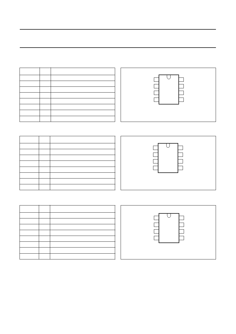
7.1
Pin description PCF8582C-2
SYMBOL
PIN
DESCRIPTION
A0
1
address input 0
A1
2
address input 1
A2
3
address input 2
V
SS
4
negative supply voltage
SDA
5
serial data input/output (I
2
C-bus)
SCL
6
serial clock input (I
2
C-bus)
PTC
7
programming time control output
V
DD
8
positive supply voltage
Fig.2 Pin configuration PCF8582C-2.
handbook, halfpage
1
2
3
4
8
7
6
5
A0
A1
A2
VSS
SDA
SCL
PTC
VDD
PCF8582C-2
MGD928
7.2
Pin description PCF8594C-2
SYMBOL
PIN
DESCRIPTION
WP
1
write-protection input
A1
2
address input 1
A2
3
address input 2
V
SS
4
negative supply voltage
SDA
5
serial data input/output (I
2
C-bus)
SCL
6
serial clock input (I
2
C-bus)
PTC
7
programming time control output
V
DD
8
positive supply voltage
Fig.3 Pin configuration PCF8594C-2.
handbook, 2 columns
1
2
3
4
8
7
6
5
WP
A1
A2
VSS
SDA
SCL
PTC
VDD
PCF8594C-2
MGL001
7.3
Pin description PCF8598C-2
SYMBOL
PIN
DESCRIPTION
WP
1
write-protection input
n.c.
2
not connected
A2
3
address input 2
V
SS
4
negative supply voltage
SDA
5
serial data input/output (I
2
C-bus)
SCL
6
serial clock input (I
2
C-bus)
PTC
7
programming time control output
V
DD
8
positive supply voltage
Fig.4 Pin configuration PCF8598C-2.
handbook, halfpage
1
2
3
4
8
7
6
5
WP
n.c.
A2
VSS
SDA
SCL
PTC
VDD
PCF8598C-2
MGL002

1997 Feb 13
7
Philips Semiconductors
Product specification
256 to 1024
◊
8-bit CMOS EEPROMs with
I
2
C-bus interface
PCF85xxC-2 family
8
I
2
C-BUS PROTOCOL
The I
2
C-bus is for 2-way, 2-line communication between
different ICs or modules. The serial bus consists of two
bidirectional lines: one for data signals (SDA), and one for
clock signals (SCL).
Both the SDA and SCL lines must be connected to a
positive supply voltage via a pull-up resistor.
The following protocol has been defined:
∑
Data transfer may be initiated only when the bus is not
busy.
∑
During data transfer, the data line must remain stable
whenever the clock line is HIGH. Changes in the data
line while the clock line is HIGH will be interpreted as
control signals.
8.1
Bus conditions
The following bus conditions have been defined:
∑
Bus not busy: both data and clock lines remain HIGH.
∑
Start data transfer: a change in the state of the data
line, from HIGH-to-LOW, while the clock is HIGH,
defines the START condition.
∑
Stop data transfer: a change in the state of the data
line, from LOW-to-HIGH, while the clock is HIGH,
defines the STOP condition.
∑
Data valid: the state of the data line represents valid
data when, after a START condition, the data line is
stable for the duration of the HIGH period of the clock
signal. There is one clock pulse per bit of data.
8.2
Data transfer
Each data transfer is initiated with a START condition and
terminated with a STOP condition. The number of the data
bytes, transferred between the START and STOP
conditions is limited to 7 bytes in the E/W mode and
8 bytes in the page E/W mode.
Data transfer is unlimited in the read mode.
The information is transmitted in bytes and each receiver
acknowledges with a ninth bit.
Within the I
2
C-bus specifications a low-speed mode (2 kHz
clock rate) and a high speed mode (100 kHz clock rate)
are defined. The PCF85xxC-2 operates in both modes.
By definition a device that sends a signal is called a
`transmitter', and the device which receives the signal is
called a `receiver'. The device which controls the signal is
called the `master'. The devices that are controlled by the
master are called `slaves'.
Each byte is followed by one acknowledge bit. This
acknowledge bit is a HIGH level, put on the bus by the
transmitter. The master generates an extra acknowledge
related clock pulse. The slave receiver which is addressed
is obliged to generate an acknowledge after the reception
of each byte.
The master receiver must generate an acknowledge after
the reception of each byte that has been clocked out of the
slave transmitter.
The device that acknowledges has to pull down the SDA
line during the acknowledge clock pulse in such a way that
the SDA line is stable LOW during the HIGH period of the
acknowledge related clock pulse.
Set-up and hold times must be taken into account.
A master receiver must signal an end of data to the slave
transmitter by not generating an acknowledge on the last
byte that has been clocked out of the slave. In this event
the transmitter must leave the data line HIGH to enable the
master generation of the STOP condition.
1997 Feb 13
8
Philips Semiconductors
Product specification
256 to 1024
◊
8-bit CMOS EEPROMs with
I
2
C-bus interface
PCF85xxC-2 family
8.3
Device addressing
Following a START condition the bus master must output
the address of the slave it is accessing. The 4 MSBs of the
slave address are the device type identifier (see Fig.5).
For the PCF85xxC-2 this is fixed to `1010'.
The next three significant bits address a particular device
or memory page (page = 256 bytes of memory). A system
could have up to eight PCF8582C-2 (or four PCF8594C-2
containing two memory pages each or two PCF8598C-2
containing four memory pages each, respectively) devices
on the bus. The eight addresses are defined by the state
of the A0, A1 and A2 inputs.
The last bit of the slave address defines the operation to
be performed. When set to logic 1 a read operation is
selected.
Address bits must be connected to either V
DD
or V
SS
.
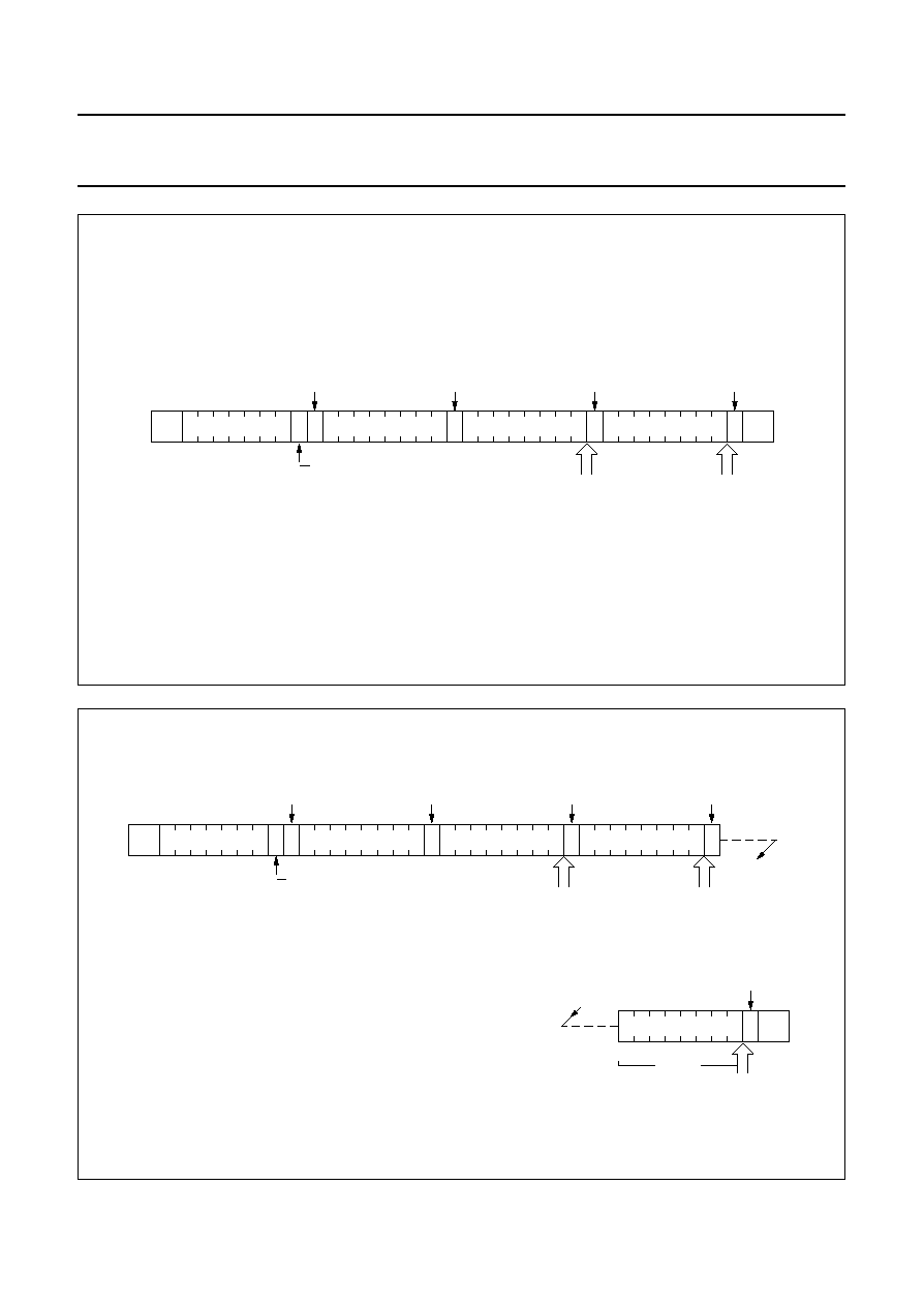
8.4
Write operations
8.4.1
B
YTE
/
WORD WRITE
For a write operation the PCF85xxC-2 requires a second
address field. This address field is a word address
providing access to the 256 words of memory. Upon
receipt of the word address the PCF85xxC-2 responds
with an acknowledge and awaits the next eight bits of data,
again responding with an acknowledge. Word address is
automatically incremented. The master can now terminate
the transfer by generating a STOP condition or transmit up
to six more bytes of data and then terminate by generating
a STOP condition.
Fig.5 Slave address.
handbook, halfpage
MBC793
1
0
1
0
A2
A1
A0 R/W
After this STOP condition the E/W cycle starts and the bus
is free for another transmission. Its duration is 10 ms per
byte.
During the E/W cycle the slave receiver does not send an
acknowledge bit if addressed via the I
2
C-bus.
8.4.2
P
AGE WRITE
The PCF85xxC-2 is capable of an eight-byte page write
operation. It is initiated in the same manner as the byte
write operation. The master can transmit eight data bytes
within one transmission. After receipt of each byte the
PCF85xxC-2 will respond with an acknowledge.
The typical E/W time in this mode is 9
◊
3.5 ms = 31.5 ms.
Erasing a block of 8 bytes in page mode takes typical
3.5 ms and sequential writing of these 8 bytes another
typical 28 ms.
After the receipt of each data byte the three low order bits
of the word address are internally incremented. The high
order five bits of the address remain unchanged. The slave
acknowledges the reception of each data byte with an
ACK. The I
2
C-bus data transfer is terminated by the
master after the 8th byte with a STOP condition. If the
master transmits more than eight bytes prior to generating
the STOP condition, no acknowledge will be given on the
ninth (and following) data bytes and the whole
transmission will be ignored and no programming will be
done. As in the byte write operation, all inputs are disabled
until completion of the internal write cycles.
8.4.3
R
EMARK
A write to the EEPROM is always performed if the pin WP
is LOW (not on PCF8582C-2). If WP is HIGH, then the
upper half of the EEPROM is write-protected and no
acknowledge will be given by the PCF85xxC-2 when one
of the upper 256 EEPROM bytes (PCF8594C-2) or
512 EEPROM bytes (PCF8598C-2) is addressed.
However, an acknowledge will be given after the slave
address and the word address.
1997 Feb 13
9
Philips Semiconductors
Product specification
256 to 1024
◊
8-bit CMOS EEPROMs with
I
2
C-bus interface
PCF85xxC-2 family
Fig.6 Auto increment memory word address; two byte write.
handbook, full pagewidth
S
0 A
SLAVE ADDRESS
WORD ADDRESS
A
A
DATA
P
acknowledge
from slave
acknowledge
from slave
acknowledge
from slave
acknowledge
from slave
A
DATA
R/W
auto increment
word address
auto increment
word address
MBA701
Fig.7 Page write operation; eight bytes.
handbook, full pagewidth
S
0 A
SLAVE ADDRESS
WORD ADDRESS
A
A
DATA N
acknowledge
from slave
acknowledge
from slave
acknowledge
from slave
R/W
auto increment
word address
acknowledge
from slave
A
DATA N + 1
auto increment
word address
MBA702
A
acknowledge
from slave
1
DATA N + 7
auto increment
word address
last byte
P
1997 Feb 13
10
Philips Semiconductors
Product specification
256 to 1024
◊
8-bit CMOS EEPROMs with
I
2
C-bus interface
PCF85xxC-2 family
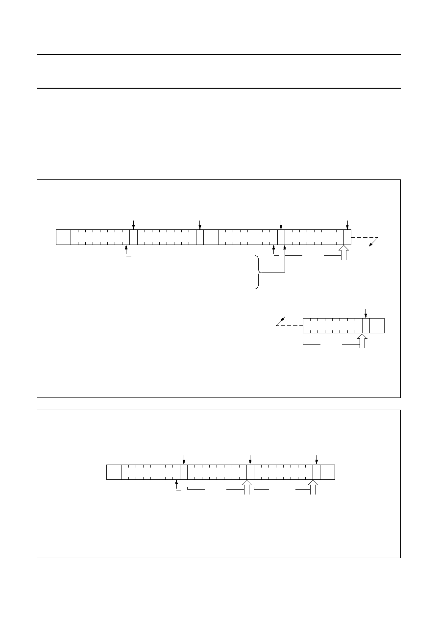
8.5
Read operations
Read operations are initiated in the same manner as write
operations with the exception that the LSB of the slave
address is set to logic 1.
There are three basic read operations; current address
read, random read and sequential read sequential read.
8.5.1
R
EMARK
The lower 8 bits of the word address are incremented after
each transmission of a data byte (read or write). The MSB
of the word address, which is defined in the slave address,
is not changed when the word address count overflows.
Thus, the word address overflows from 255 to 0 and from
511 to 256.
Fig.8 Master reads PCF85xxC-2 slave after setting word address (write word address; read data).
handbook, full pagewidth
S
0 A
SLAVE ADDRESS
WORD ADDRESS
A
A
SLAVE ADDRESS
acknowledge
from slave
acknowledge
from slave
acknowledge
from slave
R/W
acknowledge
from master
A
DATA
auto increment
word address
MBA703 - 1
P
no acknowledge
from master
1
DATA
auto increment
word address
last byte
R/W
S
1
n bytes
at this moment master
transmitter becomes
master receiver and
EEPROM slave receiver
becomes slave transmitter
Fig.9 Master reads PCF85xxC-2 immediately after first byte (read mode).
handbook, full pagewidth
S
1 A
SLAVE ADDRESS
DATA
A
1
DATA
acknowledge
from slave
acknowledge
from master
no acknowledge
from master
R/W
auto increment
word address
MBA704 - 1
auto increment
word address
n bytes
last bytes
P
1997 Feb 13
11
Philips Semiconductors
Product specification
256 to 1024
◊
8-bit CMOS EEPROMs with
I
2
C-bus interface
PCF85xxC-2 family
9
LIMITING VALUES
In accordance with the Absolute Maximum Rating System (IEC 134).
10 CHARACTERISTICS
V
DD
= 2.5 to 6.0 V; V
SS
= 0 V; T
amb
=
-
40 to +85
∞
C; unless otherwise specified.
SYMBOL
PARAMETER
CONDITIONS
MIN.
MAX.
UNIT
V
DD
supply voltage
-
0.3
+6.5
V
V
I
input voltage on any input pin
Z
i
> 500
V
SS
-
0.8
+6.5
V
I
I
input current on any input pin
-
1
mA
I
O
output current
-
10
mA
T
stg
storage temperature
-
65
+150
∞
C
T
amb
operating ambient temperature
-
40
+85
∞
C
SYMBOL
PARAMETER
CONDITIONS
MIN.
MAX.
UNIT
Supplies
V
DD
supply voltage
2.5
6.0
V
I
DDR
supply current read
f
SCL
= 100 kHz
V
DD
= 2.5 V
-
60
µ
A
V
DD
= 6.0 V
-
200
µ
A
I
DDW
supply current E/W
f
SCL
= 100 kHz
PCF8582C-2
V
DD
= 2.5 V
-
0.6
mA
V
DD
= 6.0 V
-
2.0
mA
PCF8594C-2
V
DD
= 2.5 V
-
0.8
mA
V
DD
= 6.0 V
-
2.5
mA
PCF8598C-2
V
DD
= 2.5 V
-
1.0
mA
V
DD
= 6.0 V
-
4.0
mA
I
DD(stb)
standby supply current
V
DD
= 2.5 V
-
3.5
µ
A
V
DD
= 6.0 V
-
10
µ
A
PTC output (pin 7)
V
IL
LOW level input voltage
-
0.8
0.1V
DD
V
V
IH
HIGH level input voltage
0.9V
DD
V
DD
+ 0.8 V
SCL input (pin 6)
V
IL
LOW level input voltage
-
0.8
0.3V
DD
V
V
IH
HIGH level input voltage
0.7V
DD
+6.5
V
I
LI
input leakage current
V
I
= V
DD
or V
SS
-
±
1
µ
A
f
SCL
clock input frequency
0
100
kHz
C
I
input capacitance
V
I
= V
SS
-
7
pF
1997 Feb 13
12
Philips Semiconductors
Product specification
256 to 1024
◊
8-bit CMOS EEPROMs with
I
2
C-bus interface
PCF85xxC-2 family
11 I
2
C-BUS CHARACTERISTICS
All of the timing values are valid within the operating supply voltage and ambient temperature range and refer to V
IL
and
V
IH
with an input voltage swing from V
SS
to V
DD
; see Fig.10.
Note
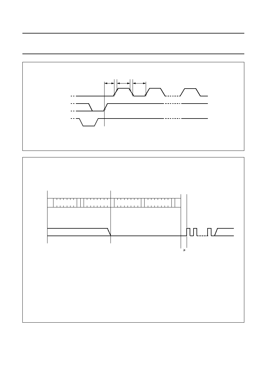
1. The hold time required (not greater than 300 ns) to bridge the undefined region of the falling edge of SCL must be
internally provided by a transmitter.
SDA input/output (pin 5)
V
IL
LOW level input voltage
-
0.8
0.3V
DD
V
V
IH
HIGH level input voltage
0.7V
DD
+6.5
V
V
OL
LOW level output voltage
I
OL
= 3 mA; V
DD(min)
-
0.4
V
I
LO
output leakage current
V
OH
= V
DD
-
1
µ
A
C
I
input capacitance
V
I
= V
SS
-
7
pF
Data retention time
t
S
data retention time
T
amb
= 55
∞
C
10
-
years
SYMBOL
PARAMETER
CONDITIONS
MIN.
MAX.
UNIT
f
SCL
clock frequency
0
100
kHz
t
BUF
bus free time between a STOP and START
condition
4.7
-
µ
s
t
HD;STA
START condition hold time after which first clock
pulse is generated
4.0
-
µ
s
t
LOW
LOW level clock period
4.7
-
µ
s
t
HIGH
HIGH level clock period
4.0
-
µ
s
t
SU;STA
set-up time for STARt condition
repeated start
4.7
-
µ
s
t
HD;DAT
data hold time
for bus compatible masters
5
-
µ
s
for bus devices
note 1
0
-
ns
t
SU;DAT
data set-up time
250
-
ns
t
r
SDA and SCL rise time
-
1
µ
s
t
f
SDA and SCL fall time
-
300
ns
t
SU;STO
set-up time for STOP condition
4.0
-
µ
s
SYMBOL
PARAMETER
CONDITIONS
MIN.
MAX.
UNIT
1997 Feb 13
13
Philips Semiconductors
Product specification
256 to 1024
◊
8-bit CMOS EEPROMs with
I
2
C-bus interface
PCF85xxC-2 family
handbook, full pagewidth
MBA705
t
BUF
HD;STA
t
SCL
SDA
P
S
t
LOW
t
r
HD;DAT
t
SU;DAT
t
t
f
t
HIGH
S
HD;STA
t
SU;STA
t
SU;STO
t
P
Fig.10 Timing requirements for the I
2
C-bus.
P
=
STOP condition;
S
=
START condition.
1997 Feb 13
14
Philips Semiconductors
Product specification
256 to 1024
◊
8-bit CMOS EEPROMs with
I
2
C-bus interface
PCF85xxC-2 family
12 WRITE CYCLE LIMITS
Selection of the chip address is achieved by connecting the A0, A1 and A2 inputs to either V
SS
or V
DD
.
13 EXTERNAL CLOCK TIMING
SYMBOL
PARAMETER
CONDITIONS
MIN.
TYP.
MAX.
UNIT
E/W cycle timing
t
E/W
E/W cycle time
internal oscillator
-
7
-
ms
external clock
4
-
10
ms
Endurance
N
E/W
E/W cycle per byte
T
amb
=
-
40 to +85
∞
C
100000
-
-
cycles
T
amb
= 22
∞
C
-
1000000
-
cycles
Fig.11 One byte E/W cycle.
handbook, full pagewidth
td
t HIGH
f
t
r
t
LOW
t
STOP
1
2
257
PTC
SDA
SCL
MBA697
Fig.12 n bytes E/W cycle (n = 2 to 7).
handbook, full pagewidth
td
t HIGH
f
t
r
t
LOW
t
STOP
1
2
PTC
SDA
SCL
MBA698
n x 256 + 1
1997 Feb 13
15
Philips Semiconductors
Product specification
256 to 1024
◊
8-bit CMOS EEPROMs with
I
2
C-bus interface
PCF85xxC-2 family
Fig.13 Page mode.
handbook, full pagewidth
td
t HIGH
f
t
r
t
LOW
t
STOP
1
2
PTC
SDA
SCL
MBA699
1153
Fig.14 External clock.
(1) If an external clock is chosen, this information is latched internally by setting pin 7 (PTC) LOW after transmission of the eighth bits of the word
address (negative edge of SCL). Thus the state of pin 7 may be previously undefined. Leaving pin 7 LOW causes a higher standby current.
(2) 1-byte programming.
(3) 2-byte programming.
(4) One page (8 bytes) programming.
handbook, full pagewidth
S
0 A
A
DATA
A
DATA
A
P
SLAVE ADDRESS
WORD ADDRESS
(1)
undefined
1
1
1
2
2
2
257
513
1153
clock (2)
clock (3)
clock (4)
d
t 0
negative edge
SCL 8-bit
undefined
LOW
HIGH
PTC
2
I C-bus
MBA700
1997 Feb 13
16
Philips Semiconductors
Product specification
256 to 1024
◊
8-bit CMOS EEPROMs with
I
2
C-bus interface
PCF85xxC-2 family
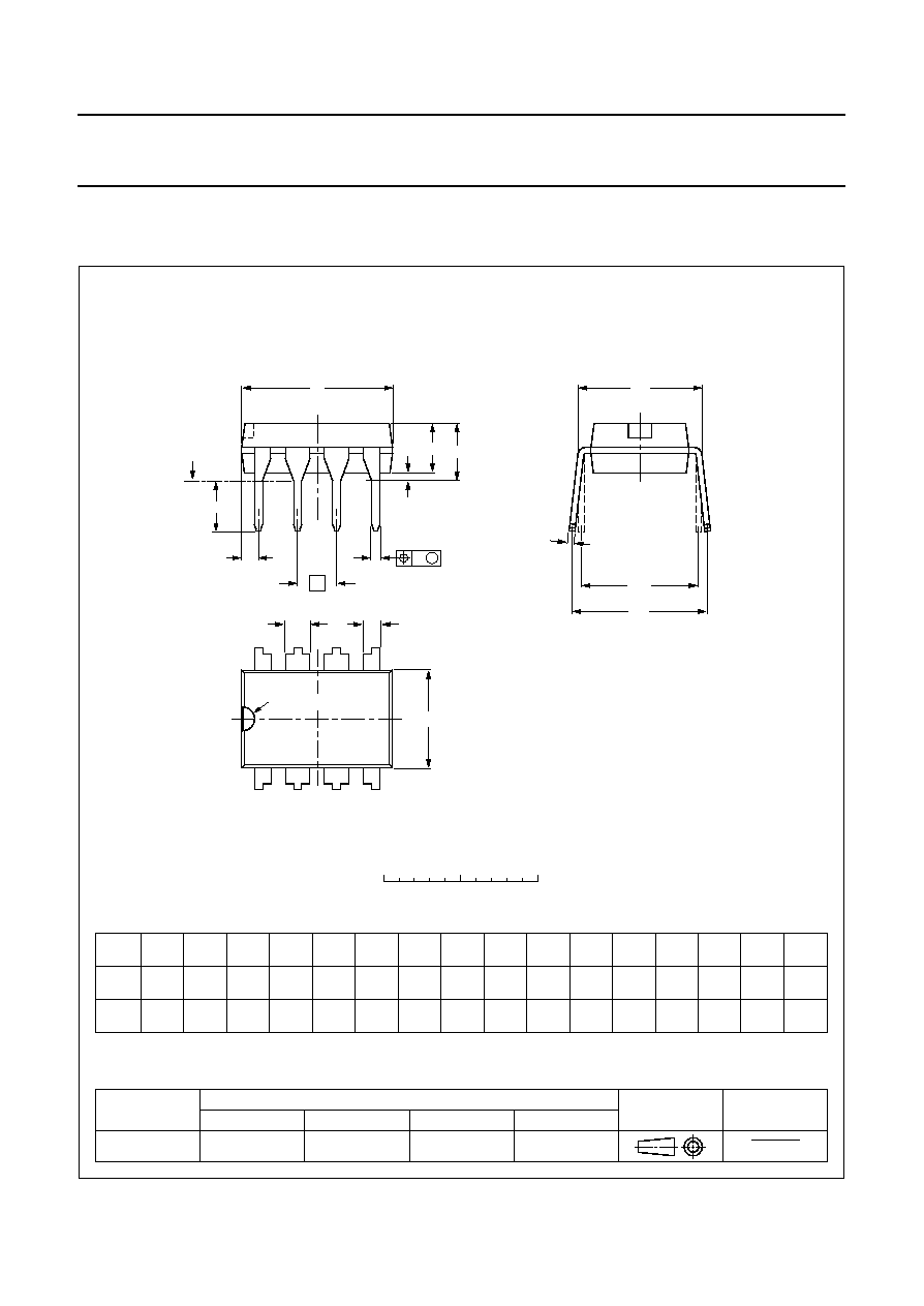
14 PACKAGE OUTLINES
REFERENCES
OUTLINE
VERSION
EUROPEAN
PROJECTION
ISSUE DATE
IEC
JEDEC
EIAJ
SOT97-1
92-11-17
95-02-04
UNIT
A
max.
1
2
b
1
(1)
(1)
(1)
b
2
c
D
E
e
M
Z
H
L
mm
DIMENSIONS (inch dimensions are derived from the original mm dimensions)
A
min.
A
max.
b
max.
w
M
E
e
1
1.73
1.14
0.53
0.38
0.36
0.23
9.8
9.2
6.48
6.20
3.60
3.05
0.254
2.54
7.62
8.25
7.80
10.0
8.3
1.15
4.2
0.51
3.2
inches
0.068
0.045
0.021
0.015
0.014
0.009
1.07
0.89
0.042
0.035
0.39
0.36
0.26
0.24
0.14
0.12
0.01
0.10
0.30
0.32
0.31
0.39
0.33
0.045
0.17
0.020
0.13
b
2
050G01
MO-001AN
M
H
c
(e )
1
M
E
A
L
seating plane
A
1
w
M
b
1
e
D
A
2
Z
8
1
5
4
b
E
0
5
10 mm
scale
Note
1. Plastic or metal protrusions of 0.25 mm maximum per side are not included.
pin 1 index
DIP8: plastic dual in-line package; 8 leads (300 mil)
SOT97-1
1997 Feb 13
17
Philips Semiconductors
Product specification
256 to 1024
◊
8-bit CMOS EEPROMs with
I
2
C-bus interface
PCF85xxC-2 family
UNIT
A
max.
A
1
A
2
A
3
b
p
c
D
(1)
E
(2)
(1)
e
H
E
L
L
p
Q
Z
y
w
v
REFERENCES
OUTLINE
VERSION
EUROPEAN
PROJECTION
ISSUE DATE
IEC
JEDEC
EIAJ
mm
inches
1.75
0.25
0.10
1.45
1.25
0.25
0.49
0.36
0.25
0.19
5.0
4.8
4.0
3.8
1.27
6.2
5.8
1.05
0.7
0.6
0.7
0.3
8
0
o
o
0.25
0.1
0.25
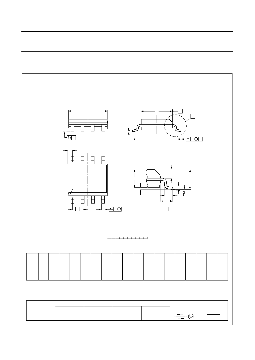
DIMENSIONS (inch dimensions are derived from the original mm dimensions)
Notes
1. Plastic or metal protrusions of 0.15 mm maximum per side are not included.
2. Plastic or metal protrusions of 0.25 mm maximum per side are not included.
1.0
0.4
SOT96-1
92-11-17
95-02-04
X
w
M
A
A
1
A
2
b
p
D
H
E
L
p
Q
detail X
E
Z
e
c
L
v
M
A
(A )
3
A
4
5
pin 1 index
1
8
y
076E03S
MS-012AA
0.069
0.0098
0.0039
0.057
0.049
0.01
0.019
0.014
0.0098
0.0075
0.20
0.19
0.16
0.15
0.050
0.24
0.23
0.028
0.024
0.028
0.012
0.01
0.01
0.041
0.004
0.039
0.016
0
2.5
5 mm
scale
SO8: plastic small outline package; 8 leads; body width 3.9 mm
SOT96-1
1997 Feb 13
18
Philips Semiconductors
Product specification
256 to 1024
◊
8-bit CMOS EEPROMs with
I
2
C-bus interface
PCF85xxC-2 family
UNIT
A
max.
A
1
A
2
A
3
b
p
c
D
(1)
E
(1)
Z
(1)
e
H
E
L
L
p
Q
y
w
v
REFERENCES
OUTLINE
VERSION
EUROPEAN
PROJECTION
ISSUE DATE
IEC
JEDEC
EIAJ
mm
inches
2.65
0.3
0.1
2.45
2.25
0.49
0.36
0.32
0.23
7.65
7.45
7.6
7.4
1.27
10.65
10.00
1.1
1.0
2.0
1.8
8
0
o
o
0.25
0.1
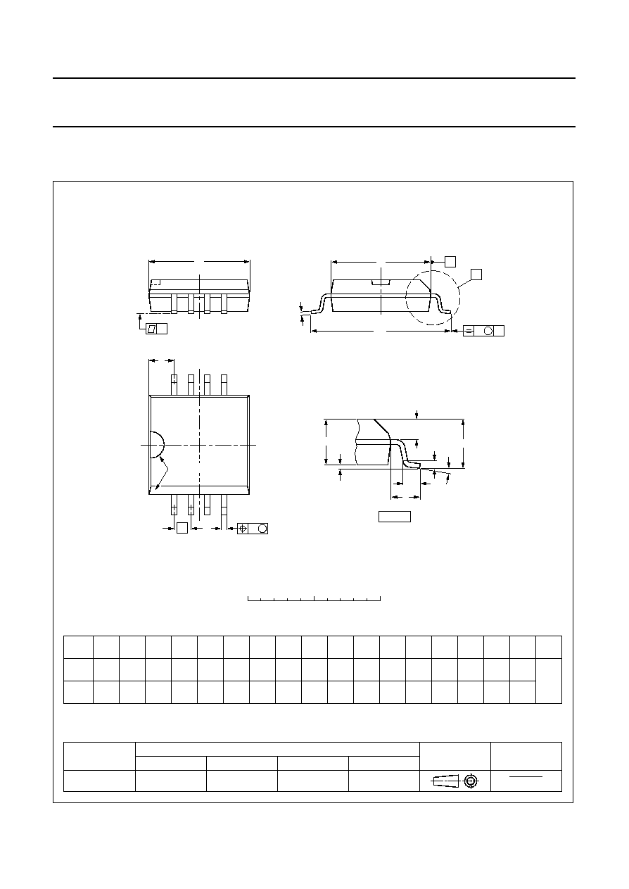
DIMENSIONS (inch dimensions are derived from the original mm dimensions)
Note
1. Plastic or metal protrusions of 0.15 mm maximum per side are not included.
1.1
0.45
SOT176-1
91-08-13
95-02-25
X
4
8
A
A
1
A
2
w
M
b
p
D
H
E
L
p
Q
detail X
E
Z
e
c
L
v
M
A
5
1
(A )
3
A
y
0.25
0.10
0.012
0.004
0.096
0.089
0.019
0.014
0.013
0.009
0.30
0.29
0.30
0.29
0.050
1.45
0.057
0.25
0.01
0.42
0.39
0.043
0.039
0.079
0.071
0.01
0.004
0.043
0.018
0.01
0
5
10 mm
scale
pin 1 index
SO8: plastic small outline package; 8 leads; body width 7.5 mm
SOT176-1

1997 Feb 13
19
Philips Semiconductors
Product specification
256 to 1024
◊
8-bit CMOS EEPROMs with
I
2
C-bus interface
PCF85xxC-2 family
15 SOLDERING
15.1
Introduction
There is no soldering method that is ideal for all IC
packages. Wave soldering is often preferred when
through-hole and surface mounted components are mixed
on one printed-circuit board. However, wave soldering is
not always suitable for surface mounted ICs, or for
printed-circuits with high population densities. In these
situations reflow soldering is often used.
This text gives a very brief insight to a complex technology.
A more in-depth account of soldering ICs can be found in
our
"IC Package Databook" (order code 9398 652 90011).
15.2
DIP
15.2.1
S
OLDERING BY DIPPING OR BY WAVE
The maximum permissible temperature of the solder is
260
∞
C; solder at this temperature must not be in contact
with the joint for more than 5 seconds. The total contact
time of successive solder waves must not exceed
5 seconds.
The device may be mounted up to the seating plane, but
the temperature of the plastic body must not exceed the
specified maximum storage temperature (T
stg max
). If the
printed-circuit board has been pre-heated, forced cooling
may be necessary immediately after soldering to keep the
temperature within the permissible limit.
15.2.2
R
EPAIRING SOLDERED JOINTS
Apply a low voltage soldering iron (less than 24 V) to the
lead(s) of the package, below the seating plane or not
more than 2 mm above it. If the temperature of the
soldering iron bit is less than 300
∞
C it may remain in
contact for up to 10 seconds. If the bit temperature is
between 300 and 400
∞
C, contact may be up to 5 seconds.
15.3
SO
15.3.1
R
EFLOW SOLDERING
Reflow soldering techniques are suitable for all SO
packages.
Reflow soldering requires solder paste (a suspension of
fine solder particles, flux and binding agent) to be applied
to the printed-circuit board by screen printing, stencilling or
pressure-syringe dispensing before package placement.
Several techniques exist for reflowing; for example,
thermal conduction by heated belt. Dwell times vary
between 50 and 300 seconds depending on heating
method. Typical reflow temperatures range from
215 to 250
∞
C.
Preheating is necessary to dry the paste and evaporate
the binding agent. Preheating duration: 45 minutes at
45
∞
C.
15.3.2
W
AVE SOLDERING
Wave soldering techniques can be used for all SO
packages if the following conditions are observed:
∑
A double-wave (a turbulent wave with high upward
pressure followed by a smooth laminar wave) soldering
technique should be used.
∑
The longitudinal axis of the package footprint must be
parallel to the solder flow.
∑
The package footprint must incorporate solder thieves at
the downstream end.
During placement and before soldering, the package must
be fixed with a droplet of adhesive. The adhesive can be
applied by screen printing, pin transfer or syringe
dispensing. The package can be soldered after the
adhesive is cured.
Maximum permissible solder temperature is 260
∞
C, and
maximum duration of package immersion in solder is
10 seconds, if cooled to less than 150
∞
C within
6 seconds. Typical dwell time is 4 seconds at 250
∞
C.
A mildly-activated flux will eliminate the need for removal
of corrosive residues in most applications.
15.3.3
R
EPAIRING SOLDERED JOINTS
Fix the component by first soldering two diagonally-
opposite end leads. Use only a low voltage soldering iron
(less than 24 V) applied to the flat part of the lead. Contact
time must be limited to 10 seconds at up to 300
∞
C. When
using a dedicated tool, all other leads can be soldered in
one operation within 2 to 5 seconds between
270 and 320
∞
C.
1997 Feb 13
20
Philips Semiconductors
Product specification
256 to 1024
◊
8-bit CMOS EEPROMs with
I
2
C-bus interface
PCF85xxC-2 family
16 DEFINITIONS
17 LIFE SUPPORT APPLICATIONS
These products are not designed for use in life support appliances, devices, or systems where malfunction of these
products can reasonably be expected to result in personal injury. Philips customers using or selling these products for
use in such applications do so at their own risk and agree to fully indemnify Philips for any damages resulting from such
improper use or sale.
18 PURCHASE OF PHILIPS I
2
C COMPONENTS
Data sheet status
Objective specification
This data sheet contains target or goal specifications for product development.
Preliminary specification
This data sheet contains preliminary data; supplementary data may be published later.
Product specification
This data sheet contains final product specifications.
Limiting values
Limiting values given are in accordance with the Absolute Maximum Rating System (IEC 134). Stress above one or
more of the limiting values may cause permanent damage to the device. These are stress ratings only and operation
of the device at these or at any other conditions above those given in the Characteristics sections of the specification
is not implied. Exposure to limiting values for extended periods may affect device reliability.
Application information
Where application information is given, it is advisory and does not form part of the specification.
Purchase of Philips I
2
C components conveys a license under the Philips' I
2
C patent to use the
components in the I
2
C system provided the system conforms to the I
2
C specification defined by
Philips. This specification can be ordered using the code 9398 393 40011.

1997 Feb 13
21
Philips Semiconductors
Product specification
256 to 1024
◊
8-bit CMOS EEPROMs with
I
2
C-bus interface
PCF85xxC-2 family
NOTES

1997 Feb 13
22
Philips Semiconductors
Product specification
256 to 1024
◊
8-bit CMOS EEPROMs with
I
2
C-bus interface
PCF85xxC-2 family
NOTES

1997 Feb 13
23
Philips Semiconductors
Product specification
256 to 1024
◊
8-bit CMOS EEPROMs with
I
2
C-bus interface
PCF85xxC-2 family
NOTES

Internet: http://www.semiconductors.philips.com
Philips Semiconductors ≠ a worldwide company
© Philips Electronics N.V. 1997
SCA53
All rights are reserved. Reproduction in whole or in part is prohibited without the prior written consent of the copyright owner.
The information presented in this document does not form part of any quotation or contract, is believed to be accurate and reliable and may be changed
without notice. No liability will be accepted by the publisher for any consequence of its use. Publication thereof does not convey nor imply any license
under patent- or other industrial or intellectual property rights.
Netherlands: Postbus 90050, 5600 PB EINDHOVEN, Bldg. VB,
Tel. +31 40 27 82785, Fax. +31 40 27 88399
New Zealand: 2 Wagener Place, C.P.O. Box 1041, AUCKLAND,
Tel. +64 9 849 4160, Fax. +64 9 849 7811
Norway: Box 1, Manglerud 0612, OSLO,
Tel. +47 22 74 8000, Fax. +47 22 74 8341
Philippines: Philips Semiconductors Philippines Inc.,
106 Valero St. Salcedo Village, P.O. Box 2108 MCC, MAKATI,
Metro MANILA, Tel. +63 2 816 6380, Fax. +63 2 817 3474
Poland: Ul. Lukiska 10, PL 04-123 WARSZAWA,
Tel. +48 22 612 2831, Fax. +48 22 612 2327
Portugal: see Spain
Romania: see Italy
Russia: Philips Russia, Ul. Usatcheva 35A, 119048 MOSCOW,
Tel. +7 095 755 6918, Fax. +7 095 755 6919
Singapore: Lorong 1, Toa Payoh, SINGAPORE 1231,
Tel. +65 350 2538, Fax. +65 251 6500
Slovakia: see Austria
Slovenia: see Italy
South Africa: S.A. PHILIPS Pty Ltd., 195-215 Main Road Martindale,
2092 JOHANNESBURG, P.O. Box 7430 Johannesburg 2000,
Tel. +27 11 470 5911, Fax. +27 11 470 5494
South America: Rua do Rocio 220, 5th floor, Suite 51,
04552-903 S„o Paulo, S√O PAULO - SP, Brazil,
Tel. +55 11 821 2333, Fax. +55 11 829 1849
Spain: Balmes 22, 08007 BARCELONA,
Tel. +34 3 301 6312, Fax. +34 3 301 4107
Sweden: Kottbygatan 7, Akalla, S-16485 STOCKHOLM,
Tel. +46 8 632 2000, Fax. +46 8 632 2745
Switzerland: Allmendstrasse 140, CH-8027 ZÐRICH,
Tel. +41 1 488 2686, Fax. +41 1 481 7730
Taiwan: Philips Semiconductors, 6F, No. 96, Chien Kuo N. Rd., Sec. 1,
TAIPEI, Taiwan Tel. +886 2 2134 2870, Fax. +886 2 2134 2874
Thailand: PHILIPS ELECTRONICS (THAILAND) Ltd.,
209/2 Sanpavuth-Bangna Road Prakanong, BANGKOK 10260,
Tel. +66 2 745 4090, Fax. +66 2 398 0793
Turkey: Talatpasa Cad. No. 5, 80640 GÐLTEPE/ISTANBUL,
Tel. +90 212 279 2770, Fax. +90 212 282 6707
Ukraine: PHILIPS UKRAINE, 4 Patrice Lumumba str., Building B, Floor 7,
252042 KIEV, Tel. +380 44 264 2776, Fax. +380 44 268 0461
United Kingdom: Philips Semiconductors Ltd., 276 Bath Road, Hayes,
MIDDLESEX UB3 5BX, Tel. +44 181 730 5000, Fax. +44 181 754 8421
United States: 811 East Arques Avenue, SUNNYVALE, CA 94088-3409,
Tel. +1 800 234 7381
Uruguay: see South America
Vietnam: see Singapore
Yugoslavia: PHILIPS, Trg N. Pasica 5/v, 11000 BEOGRAD,
Tel. +381 11 625 344, Fax.+381 11 635 777
For all other countries apply to: Philips Semiconductors, Marketing & Sales Communications,
Building BE-p, P.O. Box 218, 5600 MD EINDHOVEN, The Netherlands, Fax. +31 40 27 24825
Argentina: see South America
Australia: 34 Waterloo Road, NORTH RYDE, NSW 2113,
Tel. +61 2 9805 4455, Fax. +61 2 9805 4466
Austria: Computerstr. 6, A-1101 WIEN, P.O. Box 213,
Tel. +43 1 60 101, Fax. +43 1 60 101 1210
Belarus: Hotel Minsk Business Center, Bld. 3, r. 1211, Volodarski Str. 6,
220050 MINSK, Tel. +375 172 200 733, Fax. +375 172 200 773
Belgium: see The Netherlands
Brazil: see South America
Bulgaria: Philips Bulgaria Ltd., Energoproject, 15th floor,
51 James Bourchier Blvd., 1407 SOFIA,
Tel. +359 2 689 211, Fax. +359 2 689 102
Canada: PHILIPS SEMICONDUCTORS/COMPONENTS,
Tel. +1 800 234 7381
China/Hong Kong: 501 Hong Kong Industrial Technology Centre,
72 Tat Chee Avenue, Kowloon Tong, HONG KONG,
Tel. +852 2319 7888, Fax. +852 2319 7700
Colombia: see South America
Czech Republic: see Austria
Denmark: Prags Boulevard 80, PB 1919, DK-2300 COPENHAGEN S,
Tel. +45 32 88 2636, Fax. +45 31 57 1949
Finland: Sinikalliontie 3, FIN-02630 ESPOO,
Tel. +358 9 615800, Fax. +358 9 61580/xxx
France: 4 Rue du Port-aux-Vins, BP317, 92156 SURESNES Cedex,
Tel. +33 1 40 99 6161, Fax. +33 1 40 99 6427
Germany: Hammerbrookstraþe 69, D-20097 HAMBURG,
Tel. +49 40 23 53 60, Fax. +49 40 23 536 300
Greece: No. 15, 25th March Street, GR 17778 TAVROS/ATHENS,
Tel. +30 1 4894 339/239, Fax. +30 1 4814 240
Hungary: see Austria
India: Philips INDIA Ltd, Shivsagar Estate, A Block, Dr. Annie Besant Rd.
Worli, MUMBAI 400 018, Tel. +91 22 4938 541, Fax. +91 22 4938 722
Indonesia: see Singapore
Ireland: Newstead, Clonskeagh, DUBLIN 14,
Tel. +353 1 7640 000, Fax. +353 1 7640 200
Israel: RAPAC Electronics, 7 Kehilat Saloniki St, TEL AVIV 61180,
Tel. +972 3 645 0444, Fax. +972 3 649 1007
Italy: PHILIPS SEMICONDUCTORS, Piazza IV Novembre 3,
20124 MILANO, Tel. +39 2 6752 2531, Fax. +39 2 6752 2557
Japan: Philips Bldg 13-37, Kohnan 2-chome, Minato-ku, TOKYO 108,
Tel. +81 3 3740 5130, Fax. +81 3 3740 5077
Korea: Philips House, 260-199 Itaewon-dong, Yongsan-ku, SEOUL,
Tel. +82 2 709 1412, Fax. +82 2 709 1415
Malaysia: No. 76 Jalan Universiti, 46200 PETALING JAYA, SELANGOR,
Tel. +60 3 750 5214, Fax. +60 3 757 4880
Mexico: 5900 Gateway East, Suite 200, EL PASO, TEXAS 79905,
Tel. +9-5 800 234 7381
Middle East: see Italy
Printed in The Netherlands
417067/1200/01/pp24
Date of release: 1997 Feb 13
Document order number:
9397 750 01773