1
IDT49FCT20805
2.5V CMOS DUAL 1-TO-5 CLOCK DRIVER
INDUSTRIAL TEMPERATURE RANGE
FEBRUARY 2003
2003 Integrated Device Technology, Inc.
DSC-6172/7
c
IDT49FCT20805
ADVANCE
INFORMATION
INDUSTRIAL TEMPERATURE RANGE
2.5V CMOS DUAL
1-TO-5 CLOCK DRIVER
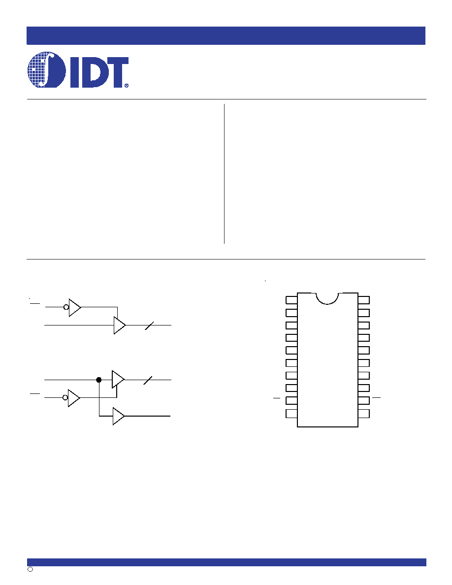
FUNCTIONAL BLOCK DIAGRAM
5
OA
1
- OA
5
OB
1
- OB
5
OE
A
IN
A
OE
B
IN
B
MON
5
PIN CONFIGURATION
OA
1
OA
3
OA
4
GND
Q
IN
A
V
CCA
OA
2
GND
A
OA
5
OE
A
1
2
3
4
5
6
7
8
9
OB
3
OB
4
MON
IN
B
V
CCB
OB
1
OB
2
GND
B
OB
5
OE
B
11
12
13
14
15
16
17
18
19
20
10
SSOP/ QSOP
TOP VIEW
FEATURES:
∑ Advanced CMOS Technology
∑ Guaranteed low skew < 200ps (max.)
∑ Very low propagation delay < 2.5ns (max)
∑ Very low duty cycle distortion < 270ps (max)
∑ Very low CMOS power levels
∑ Operating frequency up to 166MHz
∑ TTL compatible inputs and outputs
∑ Two independent output banks with 3-state control
∑ 1:5 fanout per bank
∑ "Heartbeat" monitor output
∑ V
CC
= 2.5V ± 0.2V
∑ Available in SSOP and QSOP packages
The IDT logo is a registered trademark of Integrated Device Technology, Inc.
DESCRIPTION:
The FCT20805 is a 2.5 volt clock driver built using advanced CMOS
technology. The device consists of two banks of drivers, each with a 1:5 fanout
and its own output enable control. The device has a "heartbeat" monitor for
diagnostics and PLL driving. The MON output is identical to all other outputs
and complies with the output specifications in this document. The FCT20805
offers low capacitance inputs.
The FCT20805 is designed for high speed clock distribution where signal
quality and skew are critical. The FCT20805 also allows single point-to-point
transmission line driving in applications such as address distribution, where one
signal must be distributed to multiple recievers with low skew and high signal
quality.

2
INDUSTRIAL TEMPERATURE RANGE
IDT49FCT20805
2.5V CMOS DUAL 1-TO-5 CLOCK DRIVER
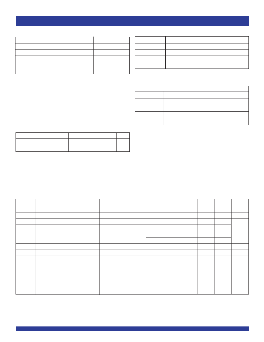
CAPACITANCE (T
A
= +25
O
C, f = 1.0MHz)
Symbol
Parameter
(1)
Conditions
Typ.
Max.
Unit
C
IN
Input Capacitance
V
IN
= 0V
3
4
pF
C
OUT
Output Capacitance
V
OUT
= 0V
--
6
pF
NOTE:
1. This parameter is measured at characterization but not tested.
PIN DESCRIPTION
Pin Names
Description
OE
A
, OE
B
3-State Output Enable Inputs (Active LOW)
IN
A
, IN
B
Clock Inputs
OAn, OBn
Clock Outputs
MON
Monitor Output
FUNCTION TABLE
(1)
Inputs
Outputs
OE
A
, OE
B
IN
A
, IN
B
OAn, OBn
MON
L
L
L
L
L
H
H
H
H
L
Z
L
H
H
Z
H
NOTE:
1. H = HIGH
L = LOW
Z = High-Impedance
ABSOLUTE MAXIMUM RATINGS
(1)
Symbol
Description
Max
Unit
V
CC
Input Power Supply Voltage
≠0.5 to +4.6
V
V
I
Input Voltage
≠0.5 to +5.5
V
V
O
Output Voltage
≠0.5 to V
CC
+0.5
V
T
J
Junction Temperature
150
∞C
T
STG
Storage Temperature
≠65 to +165
∞C
NOTE:
1. Stresses greater than those listed under ABSOLUTE MAXIMUM RATINGS may cause
permanent damage to the device. This is a stress rating only and functional operation
of the device at these or any other conditions above those indicated in the operational
sections of this specification is not implied. Exposure to absolute maximum rating
conditions for extended periods may affect reliability.
DC ELECTRICAL CHARACTERISTICS OVER OPERATING RANGE
Following Conditions Apply Unless Otherwise Specified
Industrial: T
A
= -40∞C to +85∞C, V
CC
= 2.5V ± 0.2V
Symbol
Parameter
Test Conditions
(1)
Min.
Typ.
(2)
Max.
Unit
V
IH
Input HIGH Level
1.7
--
5.5
V
V
IL
Input LOW Level
≠0.5
--
0.7
V
I
IH
Input HIGH Current
V
CC
= Max.
V
I
= 5.5V
--
--
±1
I
IL
Input LOW Current
V
CC
= Max.
V
I
= GND
--
--
±1
µA
I
OZH
High Impedance Output Current
V
CC
= Max.
V
O
= V
CC
--
--
±1
I
OZL
(3-State Outputs Pins)
V
O
= GND
--
--
±1
V
IK
Clamp Diode Voltage
V
CC
= Min., I
IN
= ≠18mA
--
≠0.7
≠1.2
V
I
ODH
Output HIGH Current
V
CC
= 2.5V, V
IN
= V
IH
or V
IL
, V
O
= 1.25V
(3,4)
≠15
≠35
≠90
mA
I
ODL
Output LOW Current
V
CC
= 2.5V, V
IN
= V
IH
or V
IL
, V
O
= 1.25V
(3,4)
25
55
100
mA
I
OS
Short Circuit Current
V
CC
= Max., V
O
= GND
(3,4)
≠30
≠50
≠120
mA
V
OH
Output HIGH Voltage
V
CC
= Min.
I
OH
= ≠8mA
1.7
(5)
--
--
V
V
IN
= V
IH
or V
IL
I
OH
= ≠100
µA
V
CC
- 0.2
--
--
V
OL
Output LOW Voltage
V
CC
= Min.
I
OL
= 8mA
--
0.2
0.4
V
V
IN
= V
IH
or V
IL
I
OL
= 100
µA
--
--
0.2
NOTES:
1. For conditions shown as Max. or Min., use appropriate value specified under Electrical Characteristics for the applicable device type.
2. Typical values are at V
CC
= 2.5V, 25∞C ambient.
3. Not more than one output should be shorted at one time. Duration of the test should not exceed one second.
4. This parameter is guaranteed but not tested.
5. V
OH
= Vcc -0.6V at rated current.

3
IDT49FCT20805
2.5V CMOS DUAL 1-TO-5 CLOCK DRIVER
INDUSTRIAL TEMPERATURE RANGE
NOTES:
1. For conditions shown as Max. or Min., use appropriate value specified under Electrical Characteristics for the applicable device type.
2. Typical values are at V
CC
= 2.5V, +25∞C ambient.
3. This parameter is not directly testable, but is derived for use in Total Power Supply calculations.
4. I
C
= I
QUIESCENT
+
I
INPUTS
+ I
DYNAMIC
I
C
= I
CC
+
I
CC
D
H
N
T
+ I
CCD
(f
O
N
O
)
I
CC
= Quiescent Current (I
CCL
, I
CCH
and I
CCZ
)
I
CC
= Power Supply Current for a TTL High Input (V
I
N
= V
CC
-0.6V)
D
H
= Duty Cycle for TTL Inputs High
N
T
= Number of TTL Inputs at D
H
I
CCD
= Dynamic Current Caused by an Input Transition Pair (HLH or LHL)
f
O
= Output Frequency
N
O
= Number of Outputs at f
O
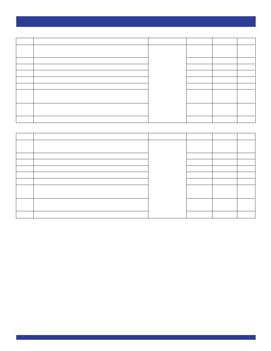
POWER SUPPLY CHARACTERISTICS
Symbol
Parameter
Test Conditions
(1)
Min.
Typ.
(2)
Max.
Unit
I
CCL
Quiescent Power Supply Current
V
CC
= Max.
--
0.1
20
µA
I
CCH
V
IN
= GND or V
CC
I
CCZ
I
CC
Power Supply Current per Input HIGH
V
CC
= Max.
--
35
250
µA
V
IN
= V
CC ≠
0.6V
I
CCD
Dynamic Power Supply Current
V
CC
= Max.
V
IN
= V
CC
--
65
100
µA/MHz
per Output
(3)
C
L
= 15pF
V
IN
= GND
All Outputs Toggling
I
C
Total Power Supply Current
(4)
V
CC
= Max.
V
IN
= V
CC
--
100
125
C
L
= 15pF
V
IN
= GND
All Outputs Toggling
V
IN
= V
CC ≠
0.6V
--
100
125
fi = 133MHz
V
IN
= GND
mA
V
CC
= Max.
V
IN
= V
CC
--
115
150
C
L
= 15pF
V
IN
= GND
All Outputs Toggling
V
IN
= V
CC ≠
0.6V
--
115
150
fi = 166MHz
V
IN
= GND

4
INDUSTRIAL TEMPERATURE RANGE
IDT49FCT20805
2.5V CMOS DUAL 1-TO-5 CLOCK DRIVER
NOTES:
1. See test circuits and waveforms.
2. Minimum limits are guaranteed but not tested on Propagation Delays.
3. t
PLH
and t
PHL
are production tested. All other parameters guaranteed but not production tested.
4. Propagation delay range indicated by Min. and Max. limit is due to V
CC
, operating temperature and process parameters. These propagation delay limits do not imply skew.
5. Skew measured between all outputs under identical transitions and load conditions.
6. Skew measured is difference between propagation delay times t
PHL
and t
PLH
of same outputs under identical load conditions.
7. Part to part skew for all outputs given identical transitions and load conditions at identical V
CC
levels and temperature.
8. Airflow of 1m/s is recommended for frequencies above 133MHz.
9. This parameter is measured using f = 1MHz.
Symbol
Parameter
Conditions
(1,8)
Min
.
(2)
Max
.
Unit
t
PLH
Propagation Delay
C
L
= 15pF
0.5
2.5
ns
t
PHL
IN
A
to OAn, IN
B
to OBn
133MHz
f 166MHz
t
R
Output Rise Time (0.7V to 1.7V)
--
1.25
ns
t
F
Output Fall Time (1.7V to 0.7V)
--
1.25
ns
t
SK(O)
Same device output pin to pin skew
(5)
--
200
ps
t
SK(P)
Pulse skew
(6,9)
--
270
ps
t
SK(PP)
Part to part skew
(7)
--
550
ps
t
PZL
Output Enable Time
--
5.2
ns
t
PZH
OE
A
to OAn, OE
B
to OBn
t
PLZ
Output Disable Time
--
5.2
ns
t
PHZ
OE
A
to OAn, OE
B
to OBn
f
MAX
Input Frequency
--
166
MHz
SWITCHING CHARACTERISTICS OVER OPERATING RANGE
(3,4)
Symbol
Parameter
Conditions
(1)
Min
.
(2)
Max
.
Unit
t
PLH
Propagation Delay
C
L
= 15pF
1
3
ns
t
PHL
IN
A
to OAn, IN
B
to OBn
f
133MHz
t
R
Output Rise Time (0.8V to 2V)
--
1.5
ns
t
F
Output Fall Time (2V to 0.8V)
--
1.5
ns
t
SK(O)
Same device output pin to pin skew
(5)
--
270
ps
t
SK(P)
Pulse skew
(6,9)
--
270
ps
t
SK(PP)
Part to part skew
(7)
--
550
ps
t
PZL
Output Enable Time
--
5.2
ns
t
PZH
OE
A
to OAn, OE
B
to OBn
t
PLZ
Output Disable Time
--
5.2
ns
t
PHZ
OE
A
to OAn, OE
B
to OBn
f
MAX
Input Frequency
--
133
MHz

5
IDT49FCT20805
2.5V CMOS DUAL 1-TO-5 CLOCK DRIVER
INDUSTRIAL TEMPERATURE RANGE
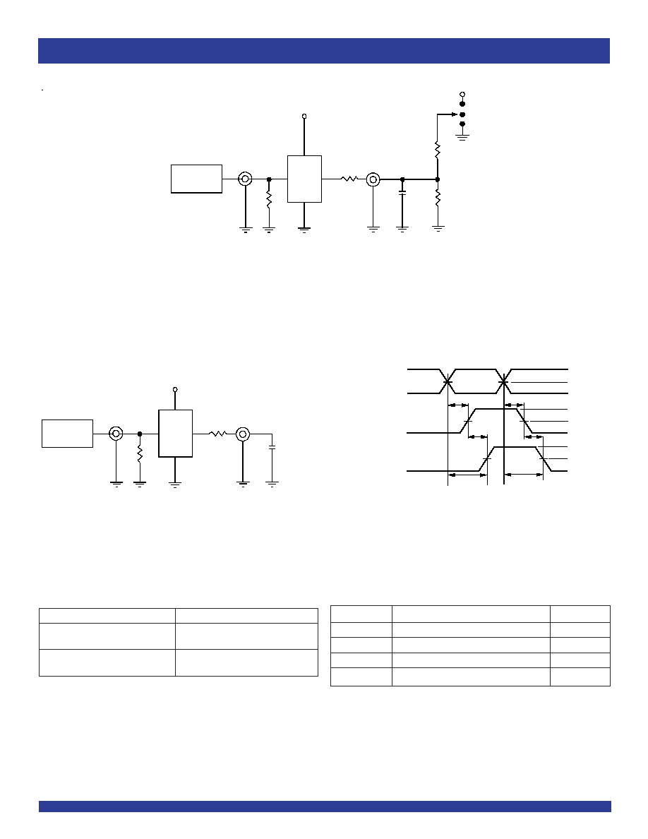
t
PLH1
OUTPUT 1
OUTPUT 2
t
SK(o)
t
PLH2
2.5V
0V
V
OH
1.25V
1.25V
V
OL
V
OH
1.25V
V
OL
INPUT
t
PHL1
t
PHL2
t
SK(o)
t
SK(o)
=
|t
PLH2 -
t
PLH1
|
or
|t
PHL2 -
t
PHL1
|
C
L
V
OUT
V
CC
Pulse
Generator
D.U.T
V
IN
R
T
R
L
V
CC
Pulse
Generator
D.U.T
V
IN
R
T
C
L
4.6V
GND
V
OUT
R
L
500
500
Open
C
L
= 15pF Test Circuit
TEST CIRCUITS AND WAVEFORMS
Enable and Disable Time Circuit
Test
Switch
Disable Low
4.6V
Enable Low
Disable High
GND
Enable High
SWITCH POSITION
Output Skew - t
SK(O)
TEST CONDITIONS
Symbol
V
CC
= 2.5V ±0.2V
Unit
C
L
15
pF
R
T
Z
OUT
of pulse generator
R
L
33
t
R
/ t
F
1 (0V to 2.5V or 2.5V to 0V)
ns
DEFINITIONS:
C
L
= Load capacitance: includes jig and probe capacitance.
R
T
= Termination resistance: should be equal to Z
OUT
of the Pulse Generator.
t
R
/ t
F
= Rise/Fall time of the input stimulus from the Pulse Generator.
