 | –≠–ª–µ–∫—Ç—Ä–æ–Ω–Ω—ã–π –∫–æ–º–ø–æ–Ω–µ–Ω—Ç: 5T940 | –°–∫–∞—á–∞—Ç—å:  PDF PDF  ZIP ZIP |

1
INDUSTRIAL TEMPERATURE RANGE
IDT5T940
PRECISION CLOCK GENERATOR
JUNE 2003
2003 Integrated Device Technology, Inc.
DSC 6195/11
c
IDT5T940
ADVANCE
INFORMATION
INDUSTRIAL TEMPERATURE RANGE
PRECISION CLOCK GENERATOR
The IDT logo is a registered trademark of Integrated Device Technology, Inc.
FEATURES:
∑ Input frequency:
- For OC non-FEC: 19.44MHz, 38.88MHz, 77.76MHz, 155.52MHz, or
311.04MHz
- For OC FEC: 20.83MHz, 41.66MHz, 83.31MHz, 166.63MHz, or
333.26MHz
- For 10GE copper: 19.53MHz, 39.06MHz, 78.125MHz, 156.25MHz, or
312.5MHz
- For 10GE optical: 20.14MHz, 40.28MHz, 80.56MHz, 161.13MHz, or
322.26MHz
∑ 3-level inputs for feedback divide ratio and output frequency range
selection
∑ 2x, 4x, 8x, 16x, and 32x outputs on Q
OUT
∑ Regenerated input clock or Q
OUT
/4 on Q
REG
∑ Lock indicator
∑ Power-down mode
∑ LVPECL or LVDS outputs
∑ Three modes of output frequency range
- Mode 0: Q
OUT
range 155.5 - 166.6MHz. Q
REG
is a regenerated version
of the input clock.
- Mode 1: Q
OUT
range 622 - 666.5MHz. Q
REG
output 155.5-166.6MHz.
- Mode 2: Q
OUT
range 622 - 666.5MHz. Q
REG
is a regenerated version
of the input clock frequency.
∑ Selectable loop bandwidths
∑ Hitless switchover
∑ Differential LVPECL, LVDS, or single-ended LVTTL input interface
∑ 2.375 - 3.465V core and I/O
∑ Available in MLF package
DESCRIPTION:
The IDT5T940 generates a high precision FEC (Forward Error Cor-
rection) or non-FEC OC-12, OC-3 source clock for SONET/SDH sys-
tems as well as a source clock for Gigabit Ethernet systems. This
device also has clock regeneration capability: it creates a "clean" ver-
sion of the clock input by using the internal oscillator to square the input
clock's rising and falling edges and remove jitter. In the event that the
main clock input fails, the device automatically locks to a backup refer-
ence clock using a hitless switchover mechanism.
This device detects loss of valid CLKIN and leaves the VCO of the PLL at
the last valid frequency while an alternate input REFIN is selected. If CLKIN
and REFIN are different frequencies, the multiplication factor will be adjusted to
retain the same output frequency.
The IDT5T940 can act as a translator from a differential LVPECL, LVDS, or
single-ended LVTTL input to LVPECL or LVDS outputs. The IDT5T940-10
has LVDS outputs and the IDT5T940-30 has LVPECL outputs.
The three modes of output frequency range are controlled by the SELmode,
which is a 3-level pin. When SELmode is high or low, the Q
OUT
is a multiplied
version of the input clock while Q
REG
is a regenerated version of the input clock.
When SELmode is mid, the Q
OUT
is a multiplied version of the input clock while
Q
REG
is Q
OUT
/4.
The IDT5T940 features a selectable loop bandwidth.
APPLICATIONS:
∑ Terabit routers
∑ Gigabit ethernet systems
∑ SONET / SDH systems
∑ Digital cross connects
∑ Optical transceiver modules
FUNCTIONAL BLOCK DIAGRAM
PLL
CONTROL
LOGIC
LOCK,
FREQ.
DETECTOR
CLKIN
REFIN
LOCK
DIV
N
DIV
M
Q
REG
Q
OUT
CLK/
REF
0
SEL
MODE
PD
PLLBW
1
PLLBW
0
INPUT
MUX
CLKIN
REFIN
CLK/
REF
1
Q
REG
Q
OUT
2
INDUSTRIAL TEMPERATURE RANGE
IDT5T940
PRECISION CLOCK GENERATOR
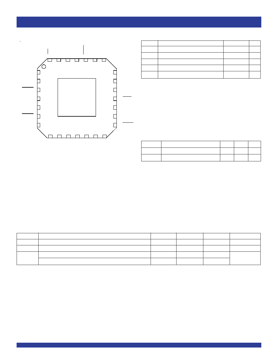
PIN CONFIGURATION
NOTE:
1. Stresses beyond those listed under ABSOLUTE MAXIMUM RATINGS may cause
permanent damage to the device. These are stress ratings only, and functional
operation of the device at these or any other conditions above those indicated in the
operational sections of this specification is not implied. Exposure to absolute-
maximum-rated conditions for extended periods may affect device reliability.
ABSOLUTE MAXIMUM RATINGS
(1)
Symbol
Description
Max
Unit
V
DD
Power Supply Voltage
≠0.5 to +4.1
V
V
I
Input Voltage
≠0.5 to +4.1
V
V
O
Output Voltage
≠0.5 to V
DD
+0.5
V
T
J
Junction Temperature
150
∞C
T
STG
Storage Temperature
≠65 to +165
∞C
NOTE:
1. Capacitance applies to all inputs except CLK/REF
[1:0]
and SELmode.
CAPACITANCE
(T
A
= +25∞C, f = 1MHz, V
IN
= 0V)
Parameter
Description
Typ.
Max.
Unit
C
IN
Input Capacitance
2.5
3
pF
C
OUT
Output Capacitance
--
--
pF
MLF
TOP VIEW
GND
CLKIN
CLKIN
GND
REFIN
REFIN
GND
V
DD
GND
Q
REG
Q
REG
LOCK
GND
V
DD
V
D
D
C
L
K
/
R
E
F
1
C
L
K
/
R
E
F
0
S
E
L
M
O
D
E
V
D
D
P
L
L
B
W
0
P
L
L
B
W
1
P
D
V
D
D
G
N
D
Q
O
U
T
Q
O
U
T
G
N
D
V
D
D
1
2
3
4
5
6
7
21
20
19
18
17
16
15
8
9
10
11
12
13
14
28
27
26
25
24
23
22
GND
Symbol
Description
Min.
Typ.
Max.
Unit
T
A
Ambient Operating Temperature
≠40
+25
+85
∞C
V
DD
Power Supply Voltage
2.375
--
3.465
V
V
T
Termination Voltage (LVPECL)
--
V
DD
≠ 2
--
V
Termination Voltage (LVDS)
--
1.2
--
RECOMMENDED OPERATING RANGE
3
INDUSTRIAL TEMPERATURE RANGE
IDT5T940
PRECISION CLOCK GENERATOR
INPUT FREQUENCY RANGE
CLK/REF
[1:0]
Input Frequency Range
H H
19.4MHz - 20.9MHz
H M
reserved
HL
38.8MHz - 41.7MHz
M H
77.7MHz - 83.4MHz
M M
Automatic Detection
ML
155.5MHz - 167MHz
LH
311MHz - 334MHz
LM
reserved
LL
reserved
PLL BANDWIDTH SELECTION
PLLBW
[1:0]
Min.
Max.
Min. CLKIN/REFIN
LL
65KHz
120KHz
19.44MHz
LH
250KHz
500KHz
19.44MHz
HL
1MHz
2MHz
38.88MHz
H H
4MHz
8MHz
155.52MHz
OUTPUT FREQUENCY RANGE
SELmode
Q
OUT
/Q
OUT
Q
REG
/Q
REG
Unit
L
155.5 - 166.6
regenerated CLKIN/CLKIN
MHz
M
622 - 666.5
155.5 - 166.6
MHz
H
622 - 666.5
regenerated CLKIN/CLKIN
MHz
PIN DESCRIPTION
Pin Name
I/O
Type
Description
CLKIN, CLKIN
I
Adjustable
(1)
Differential or single-ended clock input signal. For differential, LVPECL or LVDS supported. If left open-circuited, inputs will float
to LVTTL threshold voltage so that either input may be used as a single-ended input. A capacitor to ground should be connected
on the floating input.
REFIN, REFIN
I
Adjustable
(1)
Differential reference clock input. The reference clock input is used as an input to the PLL when CLKIN/CLKIN fails. Differential
or single-ended clock input signal. For differential, LVPECL or LVDS supported. If left open-circuited, inputs will float to LVTTL
threshold voltage so that either input may be used as a single-ended input. A capacitor to ground should be connected on the
floating input.
CLK/REF
[1:0]
I
3-level
(2)
3 level inputs controlling PLL feedback divider ratio. Automatic detection is used if both inputs are MID.
SELmode
I
3-level
(2)
3 level input to select output frequency range for Q
OUT
/Q
OUT
and Q
REG
/Q
REG
(see Output Frequency Range table)
PLLBW
[1:0]
I
LVTTL
PLL Bandwidth Select Inputs (see PLL Bandwidth Selection table)
PD
I
LVTTL
Power Down Control. Shuts off entire chip when LOW.
Q
OUT
, Q
OUT
0
Adjustable
(3)
Differential clock output. LVPECL or LVDS outputs.
Q
REG
, Q
REG
0
Adjustable
(3)
Regenerated clock output from CLKIN/CLKIN, LVPECL, or LVDS outputs.
LOCK
0
LVTTL
LOW when PLL is locked to CLKIN, HIGH in all other conditions
V
DD
PWR
Power Supply
GND
PWR
Ground
NOTES:
1. Inputs are capable of translating the following interface standards:
Single-ended 3.3V LVTTL levels
Single-ended 2.5V LVTTL levels
Differential LVPECL levels
Differential LVDS levels
2. 3-level inputs are static inputs and must be tied to V
DD
or GND or left floating.
3. Outputs can be LVPECL or LVDS.
LOCK/ FREQUENCY DETECTOR
The 5T940 will lock to, and track, a valid CLKIN signal; LOCK/ will be low
when this has occurred. If CLKIN fails, the 5T940 PLL will smoothly switch
to lock to REFIN without generating any glitches on the output. The fact that
the PLL is locked to REFIN rather than CLKIN is indicated by a high state on
LOCK/. When a valid input is then applied to CLKIN, the 5T940 will smoothly
switch back to locking on CLKIN, and LOCK/ will go low. LOCK/ will also switch
to high should the frequency of CLKIN drift close to the limits of the VCO tuning
range.
4
INDUSTRIAL TEMPERATURE RANGE
IDT5T940
PRECISION CLOCK GENERATOR
CLOCK INPUT/OUTPUT CONFIGURATION DESCRIPTION
Application
REFIN (MHz)
CKIN (MHz)
SELmode
Q
REG
(MHz)
Q
OUT
(MHz)
Non-FEC
19.44, 38.88, 77.76, 155.52
19.44
LOW
19.44
155.52
MID
155.52
622.08
HIGH
19.44
622.08
38.88
LOW
38.88
155.52
MID
155.52
622.08
HIGH
38.88
622.08
77.76
LOW
77.76
155.52
MID
155.52
622.08
HIGH
77.76
622.08
155.52
LOW
155.52
155.52
MID
155.52
622.08
HIGH
155.52
622.08
311.04
LOW
311.04
155.52
MID
155.52
622.08
HIGH
311.04
622.08
FEC
20.83, 41.66, 83.31, 166.63
20.83
LOW
20.83
166.63
MID
166.63
666.52
HIGH
20.83
666.52
41.66
LOW
41.66
166.63
MID
166.63
666.52
HIGH
41.66
666.52
83.31
LOW
83.31
166.63
MID
166.63
666.52
HIGH
83.31
666.52
166.63
LOW
166.63
166.63
MID
166.63
666.52
HIGH
166.63
666.52
333.26
LOW
333.26
166.63
MID
166.63
666.52
HIGH
333.26
666.52
10GE copper
19.53, 39.06, 78.12, 156.25
19.53
LOW
19.53
156.25
MID
156.25
625
HIGH
19.53
625
39.06
LOW
39.06
156.25
MID
156.25
625
HIGH
39.06
625
78.12
LOW
78.12
156.25
MID
156.25
625
HIGH
78.12
625
156.25
LOW
156.25
156.25
MID
156.25
625
HIGH
156.25
625
312.5
LOW
312.50
156.25
MID
156.25
625
HIGH
312.5
625
5
INDUSTRIAL TEMPERATURE RANGE
IDT5T940
PRECISION CLOCK GENERATOR
CLOCK INPUT/OUTPUT CONFIGURATION DESCRIPTION (CONTINUED)
Application
REFIN (MHz)
CKIN (MHz)
SEL mode
Q
REG
(MHz)
Q
OUT
(MHz)
10GE optical
20.14, 40.28, 80.56, 161.13
20.14
LOW
20.14
161.13
MID
161.13
644.53
HIGH
20.14
644.53
40.28
LOW
40.28
161.13
MID
161.13
644.53
HIGH
40.28
644.53
80.56
LOW
80.56
161.13
MID
161.13
644.53
HIGH
80.56
644.53
161.13
LOW
161.13
161.13
MID
161.13
644.53
HIGH
161.13
644.53
322.26
LOW
322.26
161.13
MID
161.13
644.53
HIGH
322.26
644.53
POWER SUPPLY CHARACTERISTICS
(1,2)
Symbol
Parameter
Test Conditions
Typ.
Max
Unit
I
PP
_
PD
Power Supply Current
V
DD
= Max., All outputs unloaded
--
50
µA
I
DD
Power Supply Current per Input HIGH
V
DD
= Max., V
IN
= 2.375V
--
100
µA
(LVTTL inputs only)
I
TOT
Total Power Supply Current
V
DD
= Max., Q
OUT
= 622MHz, All outputs unloaded
--
200
mA
NOTES:
1. These power consumption characteristics are for all the valid input interfaces and cover the worst case input and output interface combinations.
2. The power supply currents are not listed and are left to design to fill in as required. As a general requirement, these parts must be capable of operating at the maximum frequency
under a nominal load at a reasonable operating temperature. That means that these parts must not burn up under extended use in a typical application.
NOTE:
1. These inputs are normally wired to V
DD
, GND, or left floating. Internal termination resistors bias unconnected inputs to V
DD
/2. If these inputs are switched dynamically after powerup,
the function and timing of the outputs may be glitched, and the PLL may require additional t
AQ
time before all datasheet limits are achieved.
DC ELECTRICAL CHARACTERISTICS OVER OPERATING RANGE
Symbol
Parameter
Test Conditions
Min.
Max
Unit
V
IHH
Input HIGH Voltage Level
(1)
3-Level Inputs Only
V
DD
≠ 0.4
--
V
V
IMM
Input MID Voltage Level
(1)
3-Level Inputs Only
V
DD
/2 ≠ 0.2 V
DD
/2 + 0.2
V
V
ILL
Input LOW Voltage Level
(1)
3-Level Inputs Only
--
0.4
V
V
IN
= V
DD
HIGH Level
--
200
I
3
3-Level Input DC Current
V
IN
= V
DD
/2
MID Level
≠50
+50
µA
V
IN
= GND
LOW Level
≠200
--