 | –≠–ª–µ–∫—Ç—Ä–æ–Ω–Ω—ã–π –∫–æ–º–ø–æ–Ω–µ–Ω—Ç: 5V927 | –°–∫–∞—á–∞—Ç—å:  PDF PDF  ZIP ZIP |
1
IDT5V927
QUAD OUTPUT CLOCK GENERATOR
INDUSTRIAL TEMPERATURE RANGE
FEBRUARY 2003
2003 Integrated Device Technology, Inc.
DSC 5853/5
c
IDT5V927
INDUSTRIAL TEMPERATURE RANGE
QUAD OUTPUT
CLOCK GENERATOR
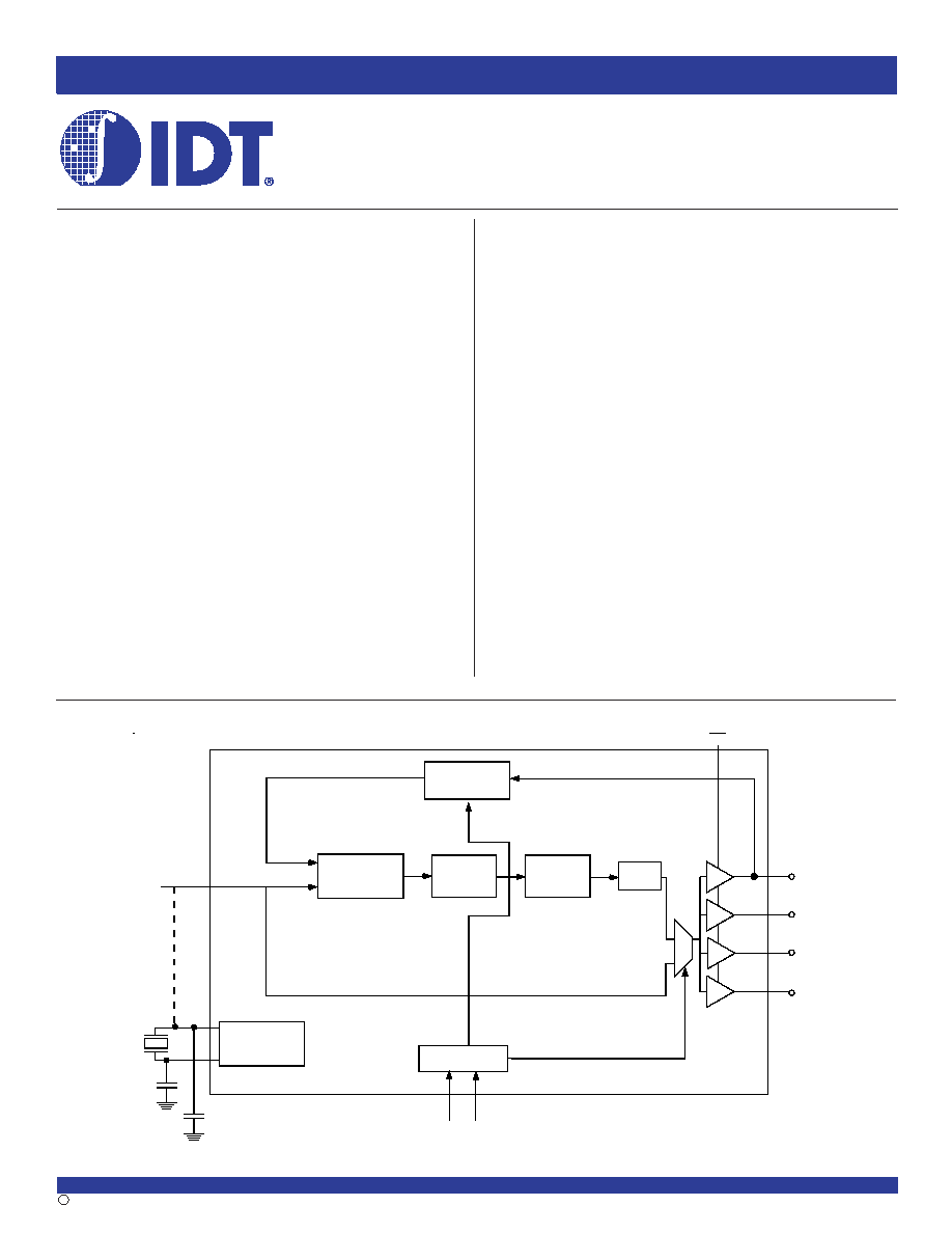
FUNCTIONAL BLOCK DIAGRAM
DESCRIPTION:
The IDT5V927 is a low-cost, low skew, low jitter, and high-performance
clock synthesizer. It has been specially designed to interface with Gigabit
Ethernet (125MHz), Fibre Channel (106.25MHz), and OC-3 (155.52MHz)
applications. It can be programmed to provide output frequencies ranging
from 50MHz to 160MHz, with input frequencies ranging from 6.25MHz to
80MHz.
The IDT5V927 includes an internal RC filter that provides excellent jitter
characteristics and eliminates the need for external components. When
using the optional crystal input, the chip accepts a 10 - 40MHz fundamental
mode crystal with a maximum equivalent series resistance of 50
.
X2
X1
CR Y ST A L
O SC ILLA T O R
P H A S E
D ET E CT OR
CH A R GE
PU M P
LOO P
FILT ER
V CO
SELE CT M O DE
Q
0
Q
3
S 1
S0
OE
0
1
Q
1
Q
2
R EF
VC O D IV ID E
1/N
FEATURES:
∑ 3V to 3.6V operating voltage
∑ 50MHz to 160MHz output frequency range
∑ Input from fundamental crystal oscillator or external source
∑ Internal PLL feedback (loading feedback output relative to
other outputs, adjusts propagation delay between REF inputs
and outputs)
∑ Select inputs (S
[1:0]
) for FB divide selection (multiply ratio of 2,
3, 4, 4.25, 5, 6, 6.25, and 8)
∑ Low jitter
∑ PLL bypass for testing and power-down control (S1 = H, S0 = H,
powers part down <500
µµ
µµ
µA)
∑ Available in TSSOP package
APPLICATIONS:
∑ Gigabit ethernet
∑ Router
∑ Network switches
∑ SAN
∑ Instrumentation
∑ Fibre channel
The IDT logo is a registered trademark of Integrated Device Technology, Inc.
2
INDUSTRIAL TEMPERATURE RANGE
IDT5V927
QUAD OUTPUT CLOCK GENERATOR
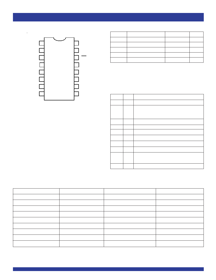
REF
X
1
X
2
V
DD
Q
0
GND
Q
1
V
DDQ
1
2
3
4
5
6
7
8
S
0
S
1
OE
GND
Q
3
GND
Q
2
V
DDQ
9
10
11
12
13
14
15
16
PIN CONFIGURATION
TSSOP
TOP VIEW
CRYSTAL SPECIFICATION
The crystal oscillators should be fundamental mode quartz crystals:
overtone crystals are not suitable. Crystal frequency should be specified
for parallel resonance with 50
maximum equivalent series resonance.
Crystal tuning capacitors should be connected from X
2
/REF to GND and from
X
1
to GND.
ABSOLUTE MAXIMUM RATINGS
(1)
Symbol
Description
Max.
Unit
V
DD
/V
DDQ
Supply Voltage to Ground
≠ 0.5 to +4.6
V
V
I
Input Voltage
≠ 0.5 to +4.6
V
I
O
Output Current
±50
mA
T
STG
Storage Temperature
≠ 65 to +150
∞C
T
J
Junction Temperature
150
∞C
NOTE:
1. Stresses greater than those listed under ABSOLUTE MAXIMUM RATINGS may cause
permanent damage to the device. This is a stress rating only and functional operation
of the device at these or any other conditions above those indicated in the operational
sections of this specification is not implied. Exposure to absolute maximum rating
conditions for extended periods may affect reliability.
PIN DESCRIPTION
Pin Name Type
Description
S[
1:0
]
I
Three level divider/mode select pins. Float to MID.
OE
I
Output enable bar. OE has a pull-down. Output Q
[1:3]
tristated
when HIGH. Output Q
0
remains running when in PLL mode
and tri-states when in TEST mode.
X
1
I
Crystal oscillator input. Connect to GND if oscillator not required.
X
2
I
Crystal oscillator output. Leave unconnected for clock input.
REF
I
Input clock. Connect to X
2
if crystal oscillator is used.
Q
[1:3]
O
Output at N*REF frequency
Q
0
O
Output at N*REF internally connected for PLL feedback
V
DDQ
PWR
Power supply for the device outputs. Connect to V
DD
on PCB.
V
DD
PWR
Power supply for the device core and inputs. Connect to V
DD
on PCB.
GND
PWR
Ground supply
NOTES:
1. H = HIGH
M = MEDIUM
L = LOW
2. Test mode for low frequency testing. In this mode, REF clock bypasses the VCO (VCO powered down) and the crystal oscillator is powered down.
DIVIDE SELECTION TABLE
(1)
S1
S0
Divide-by-N Value
Mode
L
L
2
PLL
L
M
3
PLL
L
H
4
PLL
M
L
4.25
PLL
M
M
5
PLL
M
H
6
PLL
H
L
6.25
PLL
H
M
8
PLL
H
H
TEST
TEST
(2)
3
IDT5V927
QUAD OUTPUT CLOCK GENERATOR
INDUSTRIAL TEMPERATURE RANGE
COMMON OUTPUT FREQUENCY EXAMPLES (MHz)
Output
50
60
64
72
75
80
90
100
Input
25
10
16
12
25
10
15
20
FB Divide Selection S[
1:0
]
LL
M H
LH
M H
LM
H M
M H
M M
Output
106.25
106.25
120
125
125
125
150
155.52
Input
17
25
15
20
25
62.5
25
19.44
FB Divide Selection S[
1:0
]
HL
ML
H M
HL
M M
LL
M H
H M
OPERATING CONDITIONS
Symbol
Parameter
Min.
Typ.
Max.
Unit
V
DD
/V
DDQ
Power Supply Voltage
3
3.3
3.6
V
T
A
Operating Temperature
- 40
25
+85
∞C
C
L
Output Load Capacitance
--
--
15
pF
C
IN
Input Capacitance, OE, F = 1MHz, V
IN
= 0V, T
A
= 25∞C
--
5
7
pF
DC ELECTRICAL CHARACTERISTICS OVER OPERATING RANGE
Following Conditions Apply Unless Otherwise Specified:
Industrial: T
A
= ≠40∞C to +85∞C, V
DD
/V
DDQ
= 3.3V ±0.3V
Symbol
Parameter
Test Conditions
Min.
Typ.
Max
Unit
V
IL
Input LOW Voltage
--
--
0.8
V
V
IH
Input HIGH Voltage
2
--
--
V
V
IHH
Input HIGH Voltage
3-level input only
V
DD
- 0.6
--
--
V
V
IMM
Input MID Voltage
3-level input only
V
DD
/2 - 0.3
--
V
DD
/2 + 0.3
V
V
ILL
Input LOW Voltage
3-level input only
--
--
0.6
V
I
IN
Input Leakage Current (REF input only)
V
IN
= V
DD
or GND,V
DD
= Max.
-5
--
+5
µA
V
IN
= V
DD
HIGH Level
--
--
+200
I
3
3-Level Input DC Current, S
[1:0]
V
IN
= V
DD
/2
MID Level
- 50
--
+50
µA
V
IN
= GND
LOW Level
- 200
--
--
I
IH
Input HIGH Current
V
IN
= V
DD
OE
--
--
100
µA
V
IN
= V
DD
, S
[1:0]
= HH
X
1
--
2
4
mA
V
OL
Output LOW Voltage
I
OL
= 12mA
--
--
0.4
V
V
OH
Output HIGH Voltage
I
OH
= -12mA
2.4
--
--
V

4
INDUSTRIAL TEMPERATURE RANGE
IDT5V927
QUAD OUTPUT CLOCK GENERATOR
POWER SUPPLY CHARACTERISTICS
Symbol
Parameter
Test Conditions
(1)
Min.
Typ.
Max
Unit
I
DD_PD
Power Down Current
V
DD
= Max.
--
--
500
µA
S
[1:0]
= HH
OE = L
;
REF = L; X
1
= L
All outputs unloaded
I
DD
Supply Current per Input
V
DD
= Max., V
IN
= 3V
--
--
30
µA
I
DD
Dynamic Supply Current
V
DD
= 3.6V
--
--
130
mA
S
[1:0]
= LL
OE = L
F
OUT
= 150MHz
All outputs unloaded
NOTE:
1. For conditions shown as Min. or Max., use the appropriate values specified under DC Electrical Characteristics.
INPUT TIMING REQUIREMENTS
Symbol
Description
(1)
Min.
Max.
Unit
t
R,
t
F
Maximum input rise and fall time, 0.8V to 2V
(2)
--
10
ns/V
t
PWC
Input clock pulse, HIGH or LOW
(2)
2
--
ns
D
H
Input duty cycle
(2)
10
90
%
f
OSC
XTAL oscillator frequency
--
40
MHz
f
IN
Input frequency
(2)
50/N
160/N
MHz
NOTES:
1. Where pulse width implied by D
H
is less than the t
PWC
limit, t
PWC
limit applies,
2. When using a clock input.
AC ELECTRICAL CHARACTERISTICS OVER OPERATING RANGE
Symbol
Parameter
Test Conditions
Min.
Typ.
Max.
Unit
t
R,
t
F
Rise Time, Fall Time
0.8V to 2V
--
0.7
1.5
ns
d
T
Output/Duty Cycle
V
T
= V
DDQ
/2
45
50
55
%
f
OUT
100MHz, all N
-200
--
200
t
PD
REF to Q
0
(1)
V
T
= V
DDQ
/2
50 < f
OUT
< 160MHz, N
4
-200
--
200
ps
50 < f
OUT
< 160MHz, N
4.25
-350
--
350
t
SK
Output to Output Skew (Q
0
to Q
1:3
)
Equal loads
--
--
200
ps
t
J
Cycle - Cycle Jitter
f
OUT
100MHz
-100
--
100
ps
f
OUT
Output Frequency
50
--
160
MHz
NOTE:
1. When using a clock input.
5
IDT5V927
QUAD OUTPUT CLOCK GENERATOR
INDUSTRIAL TEMPERATURE RANGE
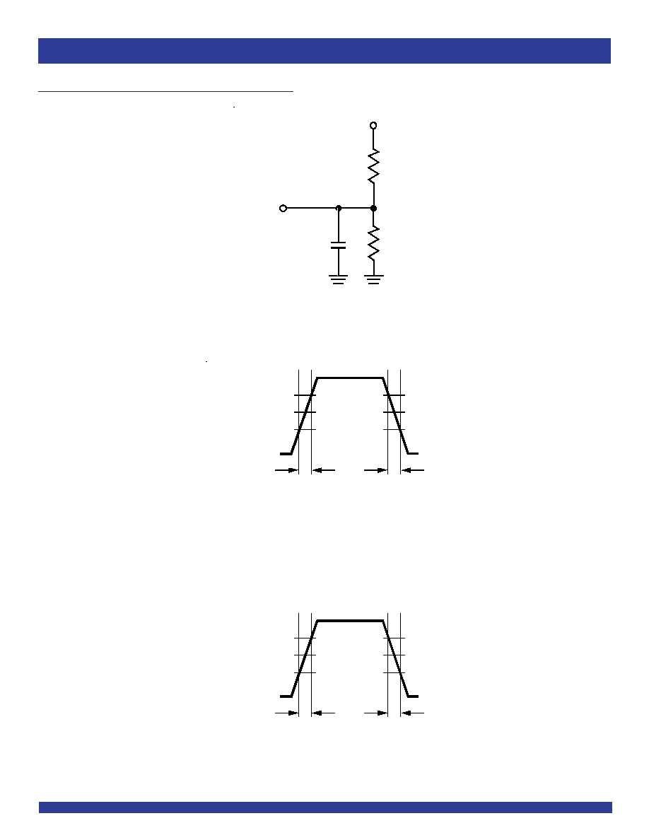
AC TEST LOADS AND WAVEFORMS
15pF
150
OUTPUT
V
DD
150
2V
V
TH
= V
D D
/2
0V
1ns
3V
1ns
0.8
2V
0V
t
R
t
F
0.8
V
D D Q
V
TH
= V
D DQ
/2
AC Test Load
Input Test Waveform
Output Waveform
6
INDUSTRIAL TEMPERATURE RANGE
IDT5V927
QUAD OUTPUT CLOCK GENERATOR
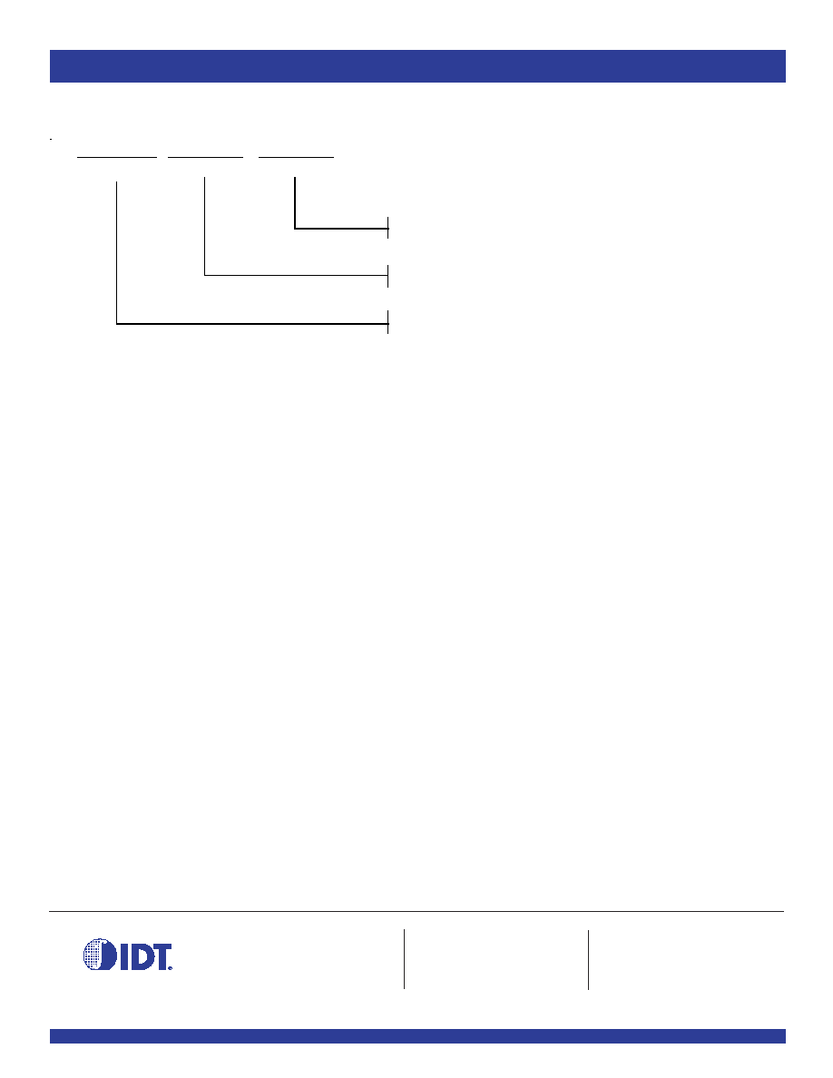
ORDERING INFORMATION
IDT
XXXX
X
Package
Thin Shrink Small Outline Package
PG
Device Type
5V927
Quad Output Clock Generator
X
Package
Industrial Temperature Range (-40∞C to +85∞C)
I
CORPORATE HEADQUARTERS
for SALES:
for Tech Support:
2975 Stender Way
800-345-7015 or 408-727-6116
logichelp@idt.com
Santa Clara, CA 95054
fax: 408-492-8674
(408) 654-6459
www.idt.com