Document Outline
- Features
- Description
- Functional Block Diagram
- Pin Configuration
- Pin Description
- PLL Features and Descriptions
- Reference Clock Inputs Pins and Selection
- Pre-Scaler, Feedback-Divider, and Post-Divider
- Pre-Scaler
- Feedback-Divider
- Post-Divider
- Post-Divider Diagram
- Spread Spectrum Generation
- Sinusoidal with Down Spread
- Fractional Divider
- Loop Filter
- Charge Pump and Loop Filter Configuration
- Configuring the Multi-Purpose I/Os
- Mode 1 - MFC Mode for PLL0
- Mode 2 - MFC Mode for all PLLs
- Mode 3 - I2C Programming Mode
- Mode 4 - JTAG Programming Mode
- Manual Frequency Control Mode
- Understanding the GIN Signals
- Shutdown/Suspend/Enable of Outputs
- MFC Block Diagrams
- Block Diagram for Shurdown/OE Control Signal
- Power Up and Power Saving Features
- Loss of Lock and Input Clock
- Switchover Modes
- Manual Switchover Mode
- Automatic Switchover Mode
- Clock Switch Matrix and Outputs
- High Level Block Diagram for Configuration
- Programming the Device
- I2C Programming
- Fig 1: Framing Diagram
- Fig 2: First Byte Transmitted on I2C Bus
- External I2C Interface Condition
- Progwrite
- Progread
- Progsave
- Progrestore
- JTAG Interface
- JTAG Instruction Register Description
- EEPROM Interface
- I2C Bus DC Characteristics
- I2C Bus AC Characteristics for Standard Mode
- I2C Bus AC Characteristics for Fast Mode
- Absolute Maximum Ratings
- Capacitance
- Recommended Operating Conditions
- DC Electrical Characteristics
- DC Electrical Characteristics for 3.3V LVTTL
- Power Supply Characteristics for LVTTL
- DC Electrical Characteristics for LVDS
- Power Supply Characteristics for LVDS
- DC Electrical Characteristics for LVPECL
- Power Supply Characteristics for LVPECL
- AC Timing Electrical Characteristics
- Spread Spectrum Generation Specs
- Test Circuits and Conditions
- Other Termination Scheme
- RAM (Programming Register) Tables
- Recommended Landing Pattern
- Ordering Information

1
INDUSTRIAL TEMPERATURE RANGE
IDT5V9885
3.3V EEPROM PROGRAMMABLE CLOCK GENERATOR
APRIL 2005
2005 Integrated Device Technology, Inc.
DSC 6787/21
c
IDT5V9885
ADVANCE
INFORMATION
INDUSTRIAL TEMPERATURE RANGE
3.3V EEPROM
PROGRAMMABLE CLOCK
GENERATOR
The IDT logo is a registered trademark of Integrated Device Technology, Inc.
FEATURES:
� Three internal PLLs
� Internal non-volatile EEPROM
� JTAG and FAST mode I
2
C serial interfaces
� Input Frequency Ranges: 1MHz to 400MHz
� Output Frequency Ranges: 4.9kHz to 550MHz
� Reference Crystal Input with programmable oscillator gain and
programmable linear load capacitance
- Crystal Frequency Range: 8MHz to 50MHz
� Each PLL has an 8-bit pre-scaler and a 12-bit feedback-divider
� 10-bit post-divider blocks
� Fractional Dividers
� Two of the PLLs support Spread Spectrum Generation
capability
� I/O Standards:
- Outputs - 3.3V LVTTL/ LVCMOS, LVPECL, and LVDS
- Inputs - 3.3V LVTTL/ LVCMOS
� Programmable Slew Rate Control
� Programmable Loop Bandwidth Settings
� Programmable output inversion to reduce bimodal jitter
� Redundant clock inputs with glitchless auto and manual
switchover options
� JTAG Boundary Scan
� Individual output enable/disable
� Power-down mode
� 3.3V V
DD
� Available in TQFP and VFQFPN packages
DESCRIPTION:
The IDT5V9885 is a programmable clock generator intended for high
performance data-communications, telecommunications, consumer, and
networking applications. There are three internal PLLs, each individually
programmable, allowing for three unique non-integer-related frequencies.
The frequencies are generated from a single reference clock. The
reference clock can come from one of the two redundant clock inputs. A
glitchless automatic or manual switchover function allows any one of the
redundant clocks to be selected during normal operation.
The IDT5V9885 can be programmed through the use of the I
2
C or JTAG
interfaces. The programming interface enables the device to be pro-
grammed when it is in normal operation or what is commonly known as in-
system programmable. An internal EEPROM allows the user to save and
restore the configuration of the device without having to reprogram it on
power-up. JTAG boundary scan is also implemented.
Each of the three PLLs has an 8-bit pre-scaler and a 12-bit feedback
divider. This allows the user to generate three unique non-integer-related
frequencies. The PLL loop bandwidth is programmable to allow the user
to tailor the PLL response to the application. For instance, the user can tune
the PLL parameters to minimize jitter generation or to maximize jitter
attenuation. Spread spectrum generation and fractional divides are
allowed on two of the PLLs.
There are also 10-bit post dividers on five of the six output banks. Two
of the six output banks are configurable to be LVTTL, LVPECL, or LVDS.
The other four output banks are LVTTL. The outputs are connected to the
PLLs via the switch matrix. The switch matrix allows the user to route the
PLL outputs to any output bank. This feature can be used to simplify and
optimize the board layout. In addition, each output's slew rate and enable/
disable function can be programmed.
2
INDUSTRIAL TEMPERATURE RANGE
IDT5V9885
3.3V EEPROM PROGRAMMABLE CLOCK GENERATOR
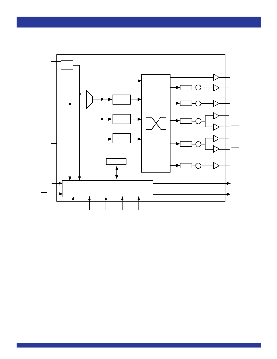
FUNCTIONAL BLOCK DIAGRAM
EEPROM
Control Block for
Multi-Purpose I/O, Programming, Features
OSC.
PLL 0
PLL 1
PLL 2
10-Bit
P2 Divider
10-Bit
P6 Divider
10-Bit
P3 Divider
10-Bit
P4 Divider
10-Bit
P5 Divider
XTALOUT
XTALIN/REF_IN
CLK_IN
SHUTDOWN/OE
GIN5/CLK_SEL
I C/JTAG
2
G
I
N
0
/
S
D
A
T
/
T
D
I
G
I
N
1
/
S
C
L
K
/
T
C
L
K
G
I
N
2
/
T
M
S
G
I
N
3
/
S
U
S
P
E
N
D
G
I
N
4
/
T
R
S
T
/2
/2
OUT1
OUT3
OUT4
OUT4
OUT5
OUT5
OUT2
OUT6
GOUT0/TDO/
LOSS_LOCK
GOUT1/
LOSS_CLKIN
(1)
(1)
(1)
(1)
/2
/2
/2
NOTE:
1. OUT4 and OUT5 pairs can be configured to be LVDS, LVPECL, or two single-ended LVTTL outputs. As LVTTL, OUT4 and OUT5 can be configured to be non-inverting.
3
INDUSTRIAL TEMPERATURE RANGE
IDT5V9885
3.3V EEPROM PROGRAMMABLE CLOCK GENERATOR
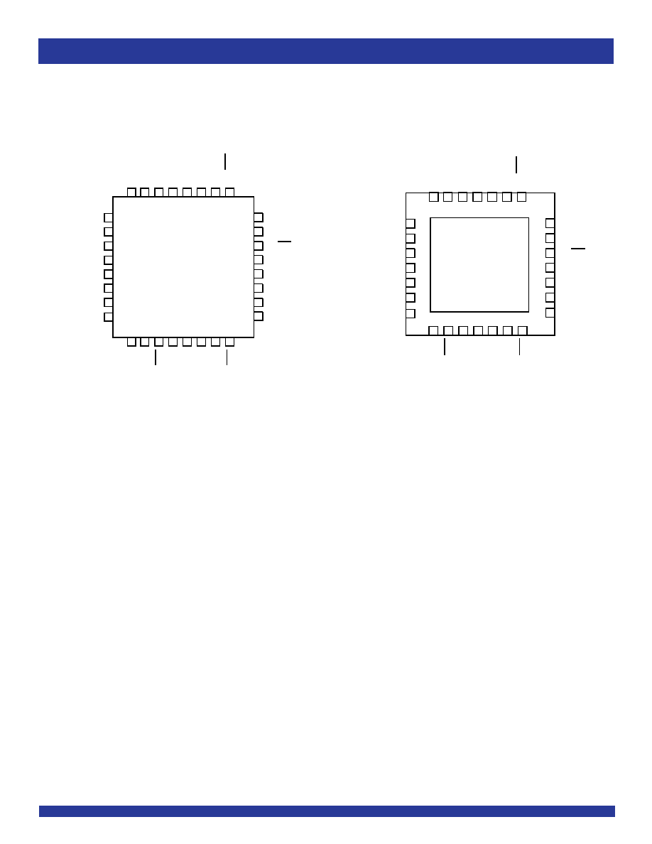
PIN CONFIGURATION
31
10
O
U
T
4
30
29
28
27
26
25
11
12
13
14
15
16
G
O
U
T
0
.
T
D
O
/
L
O
S
S
_
L
O
C
K
O
U
T
2
S
H
U
T
D
O
W
N
/
O
E
G
I
N
3
/
S
U
S
P
E
N
D
V
D
D
O
U
T
4
O
U
T
6
O
U
T
5
O
U
T
5
V
D
D
G
N
D
G
N
D
32
9
V
D
D
G
N
D
G
I
N
4
/
T
R
S
T
1
2
3
4
5
6
7
8
CLKIN
GND
GOUT1/LOSS_CLKIN
XTALIN/REF_IN
OUT1
V
DD
OUT3
XTALOUT
18
GND
24
23
22
21
20
19
I C/JTAG
GIN2/TMS
AV
DD
GIN1/SCLK/TCLK
GIN0/SDA/TDI
GIN5/CLK_SEL
17
V
DD
2
TQFP
TOP VIEW
27
26
25
24
23
22
G
O
U
T
0
.
T
D
O
/
L
O
S
S
_
L
O
C
K
O
U
T
2
S
H
U
T
D
O
W
N
/
O
E
G
I
N
3
/
S
U
S
P
E
N
D
G
N
D
28
V
D
D
G
I
N
4
/
T
R
S
T
8
O
U
T
4
9
10
11
12
13
14
O
U
T
4
O
U
T
6
O
U
T
5
O
U
T
5
V
D
D
G
N
D
1
2
3
4
5
6
7
CLKIN
GND
GOUT1/LOSS_CLKIN
XTALIN/REF_IN
OUT1
OUT3
XTALOUT
21
20
19
18
17
16
I C/JTAG
GIN2/TMS
AV
DD
GIN1/SCLK/TCLK
GIN0/SDA/TDI
GIN5/CLK_SEL
15
V
DD
2
GND
VFQFPN
TOP VIEW

4
INDUSTRIAL TEMPERATURE RANGE
IDT5V9885
3.3V EEPROM PROGRAMMABLE CLOCK GENERATOR
PIN DESCRIPTION
PF32
NL28
Pin Name
Pin#
Pin#
I/O
Type
Description
CLK_IN
1
1
I
LVTTL
Input Clock
XTALIN/REF_IN
4
4
I
LVTTL
CRYSTAL_IN - Reference crystal input or external reference clock input
XTALOUT
5
5
O
LVTTL
CRYSTAL_OUT -Reference crystal feedback
GIN0/SDAT/TDI
19
16
I
LVTTL
(3)
Multi-purpose inputs. Can be used for Frequency Control, SDAT(I
2
C), or TDI(JTAG).
GIN1/SCLK/TCK
20
17
I
LVTTL
(3)
Multi-Purpose inputs. Can be used for Frequency Control, SCLK(I
2
C), or TCK(JTAG).
GIN2/TMS
24
21
I
LVTTL
(3)
Multi-Purpose inputs. Can be used for Frequency Control or TMS (JTAG)
GIN3/SUSPEND
27
23
I
LVTTL
(3)
Multi-Purpose inputs. Can be used for Frequency Control or as a suspend mode control
input (active HIGH).
GIN4/TRST
25
22
I
LVTTL
(3)
Multi-Purpose inputs. Can be used for Frequency Control or TRST (JTAG)
GIN5/CLK_SEL
21
18
I
LVTTL
(3)
Multi-Purpose inputs. Can be used for Frequency Control or input clock selector.
SHUTDOWN/OE
28
24
I
LVTTL
(3)
Enables/disables the outputs or powers down the chip. The SP bit (0x1C) controls the
polarity of the signal to be either active HIGH or LOW. (Default is active HIGH.)
I
2
C/JTAG
22
19
I
3-level
(2)
I
2
C (HIGH) or MFC Mode (MID) or JTAG Programming (LOW)
OUT1
6
6
O
LVTTL
Configurable clock output 1. Can also be used to buffer the reference clock.
OUT2
29
25
O
LVTTL
Configurable clock output 2
OUT3
8
7
O
LVTTL
Configurable clock output 3
OUT4
10
8
O
Adjustable
(1)
Configurable clock output 4, Single-Ended or Differential when combined with OUT4
OUT4
11
9
O
Adjustable
(1)
Configurable complementary clock output 4, Single-Ended or Differential when
combined with OUT4
OUT5
15
13
O
Adjustable
(1)
Configurable clock output 5, Single-Ended or Differential when combined with OUT5
OUT5
16
14
O
Adjustable
(1)
Configurable complementary clock output 5, Single-Ended or Differential when
combined with OUT5
OUT6
13
11
O
LVTTL
Configurable clock output 6
GOUT0/TDO/LOSS_LOCK
31
27
O
LVTTL
(3)
Multi-Purpose Output. Can be programmed to use as PLL LOCK signal, LOSS_LOCK
or TDO in JTAG mode
GOUT1/LOSS_CLKIN
3
3
O
LVTTL
Multi-Purpose Output. Can be programmed to use as LOSS_CLKIN
V
DD
7,12,17,
10,15,28
Power Supply for the output buffers
26,32
AV
DD
23
20
Analog power supply
GND
2,9,14,
2,12,26
Ground
18,30
NOTES:
1. Outputs are user programmable to drive single-ended 3.3V LVTTL, differential LVDS, or differential LVPECL interface levels.
2. 3-level inputs are static inputs and must be tied to V
DD
or GND or left floating. These inputs are internally biased to V
DD
/2. They are not hot-insertable or over voltage tolerant.
3. The JTAG (TDO, TMS, TCLK, TRST, and TDI) and I
2
C (SCLK and SDAT) signals share the same pins with GIN signals.
5
INDUSTRIAL TEMPERATURE RANGE
IDT5V9885
3.3V EEPROM PROGRAMMABLE CLOCK GENERATOR
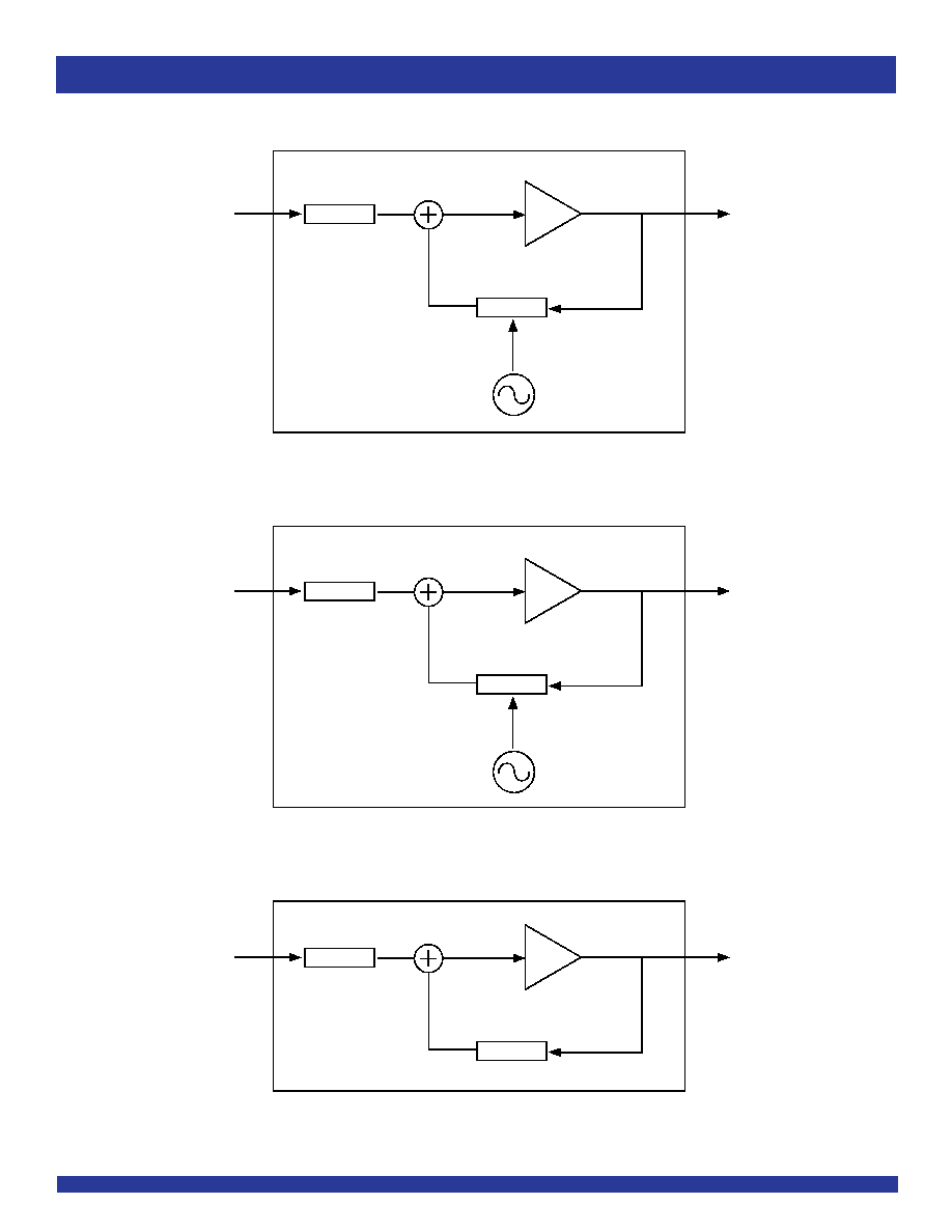
PLL FEATURES AND DESCRIPTIONS
/ 8-bit
/ 12-bit
VCO
D0 Divider
M0 Multiplier
Spread
Spectrum
Modulation
/ 8-bit
/ 12-bit
VCO
D1 Divider
M1 Multiplier
Spread
Spectrum
Modulation
/ 8-bit
/ 12-bit
VCO
D2 Divider
M2 Multiplier
PLL2 Block Diagram
PLL0 Block Diagram
PLL1 Block Diagram