 | –≠–ª–µ–∫—Ç—Ä–æ–Ω–Ω—ã–π –∫–æ–º–ø–æ–Ω–µ–Ω—Ç: 5V9910A | –°–∫–∞—á–∞—Ç—å:  PDF PDF  ZIP ZIP |
1
COMMERCIAL AND INDUSTRIAL TEMPERATURE RANGES
IDT5V9910A
3.3V LOW SKEW PLL CLOCK DRIVER TURBOCLOCK JR.
SEPTEMBER 2001
2001 Integrated Device Technology, Inc.
DSC 5847/1
c
COMMERCIAL AND INDUSTRIAL TEMPERATURE RANGES
The IDT logo is a registered trademark of Integrated Device Technology, Inc.
FEATURES:
∑ Eight zero delay outputs
∑ <250ps of output to output skew
∑ Selectable positive or negative edge synchronization
∑ Synchronous output enable
∑ Output frequency: 15MHz to 85MHz
∑ 3 skew grades:
IDT5V9910A-2: t
SKEW0
<250ps
IDT5V9910A-5: t
SKEW0
<500ps
IDT5V9910A-7: t
SKEW0
<750ps
∑ 3-level inputs for PLL range control
∑ PLL bypass for DC testing
∑ External feedback, internal loop filter
∑ 12mA balanced drive outputs
∑ Low Jitter: <200ps peak-to-peak
∑ Available in SOIC package
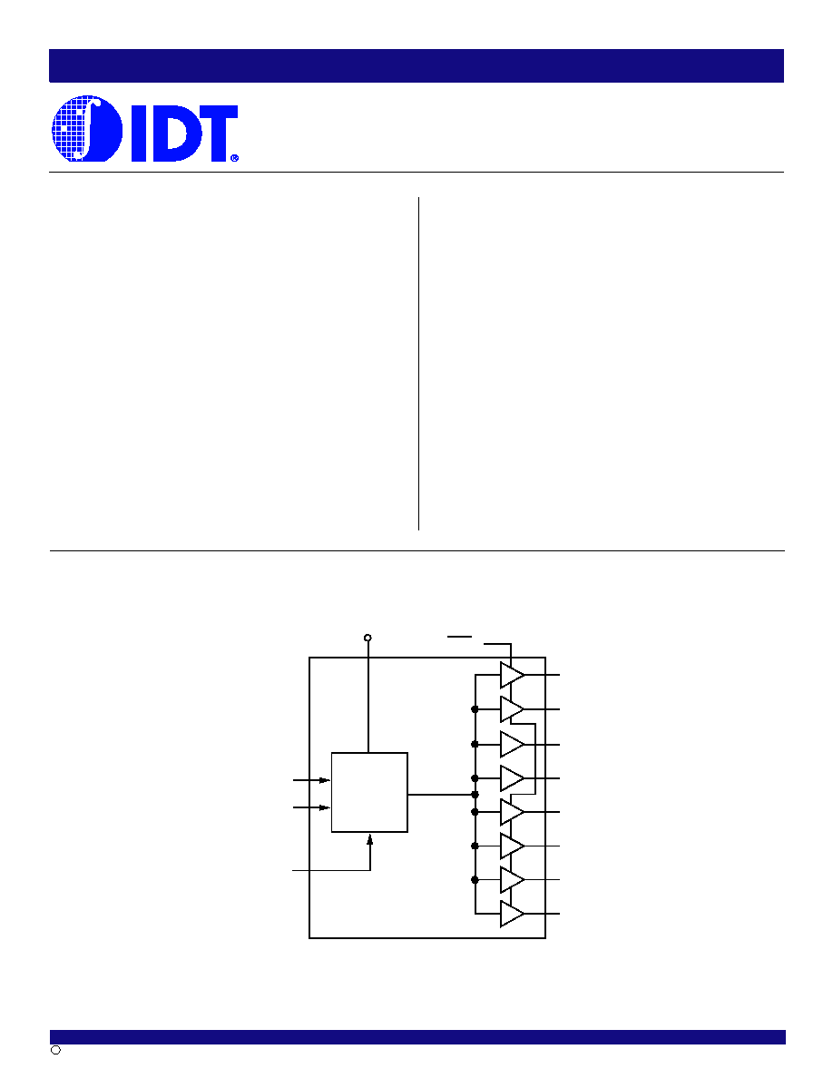
FUNCTIONAL BLOCK DIAGRAM
G ND/sO E
Q
0
Q
1
REF
FS
PLL
FB
V
CCQ
/PE
Q
2
Q
3
Q
4
Q
5
Q
6
Q
7
IDT5V9910A
3.3V LOW SKEW
PLL CLOCK DRIVER
TURBOCLOCKTM JR.
DESCRIPTION:
The IDT5V9910A is a high fanout phase locked-loop clock driver
intended for high performance computing and data-communications appli-
cations. It has eight zero delay LVTTL outputs.
When the GND/
sOE pin is held low, all the outputs are synchronously
enabled. However, if GND/
sOE is held high, all the outputs except Q
2
and
Q
3
are synchronously disabled.
Furthermore, when the V
CCQ
/PE is held high, all the outputs are
synchronized with the positive edge of the REF clock input. When V
CCQ
/
PE is held low, all the outputs are synchronized with the negative edge of
REF.
The FB signal is compared with the input REF signal at the phase detector
in order to drive the VCO. Phase differences cause the VCO of the PLL to
adjust upwards or downwards accordingly.
An internal loop filter moderates the response of the VCO to the phase
detector. The loop filter transfer function has been chosen to provide minimal
jitter (or frequency variation) while still providing accurate responses to input
frequency changes.

2
COMMERCIAL AND INDUSTRIAL TEMPERATURE RANGES
IDT5V9910A
3.3V LOW SKEW PLL CLOCK DRIVER TURBOCLOCK JR.
PIN CONFIGURATION
NOTE:
1. Stresses beyond those listed under ABSOLUTE MAXIMUM RATINGS may cause
permanent damage to the device. These are stress ratings only, and functional
operation of the device at these or any other conditions above those indicated in the
operational sections of this specification is not implied. Exposure to absolute-
maximum-rated conditions for extended periods may affect device reliability.
ABSOLUTE MAXIMUM RATINGS
(1)
Symbol
Description
Max
Unit
Supply Voltage to Ground
≠0.5 to +7
V
V
I
DC Input Voltage
≠0.5 to V
CC
+0.5
V
REF Input Voltage
≠0.5 to +5.5
V
Maximum Power Dissipation (T
A
= 85∞C)
530
mW
T
STG
Storage Temperature
≠65 to +150
∞ C
NOTE:
1. Capacitance applies to all inputs except TEST and FS. It is characterized but not
production tested.
CAPACITANCE
(T
A
= +25∞C, f = 1MHz, V
IN
= 0V)
Parameter
Description
Typ.
Max.
Unit
C
IN
Input Capacitance
5
7
pF
PIN DESCRIPTION
Pin Name
Type
Description
REF
I N
Reference Clock Input
FB
I N
Feedback Input
TEST
(1)
I N
When MID or HIGH, disables PLL (except for conditions of Note 1). REF goes to all outputs. Set LOW for normal operation.
GND/
sOE
(1)
I N
Synchronous Output Enable. When HIGH, it stops clock outputs (except Q
2
and Q
3
) in a LOW state - Q
2
and Q
3
may be used as the
feedback signal to maintain phase lock. Set GND/
sOE LOW for normal operation.
V
CCQ
/PE
I N
Selectable positive or negative edge control. When LOW/HIGH the outputs are synchronized with the negative/positive edge of the
reference clock.
FS
(2)
I N
Frequency range select:
FS = GND: 15 to 35MHz
FS = MID (or open): 25 to 60MHz
FS = V
CC
: 40 to 85MHz
Q
0
- Q
7
OUT
Eight clock output
V
CCN
PWR
Power supply for output buffers
V
CCQ
PWR
Power supply for phase locked loop and other internal circuitry
GND
PWR
Ground
SOIC
TOP VIEW
NOTES:
1. When TEST = MID and GND/
sOE = HIGH, PLL remains active.
2. This input is wired to Vcc, GND, or unconnected. Default is MID level. If it is switched in the real time mode, the outputs may glitch, and the PLL may require an additional
lock time before all data sheet limits are achieved.
1
2
3
4
5
6
7
8
9
10
11
12
24
23
22
21
20
19
18
17
16
15
14
13
R E F
FS
N C
V
C C Q
/P E
Q
0
Q
1
G N D
Q
2
Q
3
G N D
TE ST
N C
G N D /sO E
Q
7
Q
6
G N D
Q
5
Q
4
FB
V
C C N
V
C C N
V
C C Q
V
C C N
V
C C N

3
COMMERCIAL AND INDUSTRIAL TEMPERATURE RANGES
IDT5V9910A
3.3V LOW SKEW PLL CLOCK DRIVER TURBOCLOCK JR.
RECOMMENDED OPERATING RANGE
IDT5V9910A-5, -7
IDT5V9910A-2
(Industrial)
(Commercial)
Symbol
Description
Min.
Max.
Min.
Max.
Unit
V
CC
Power Supply Voltage
3
3.6
3
3.6
V
T
A
Ambient Operating Temperature
-40
+85
0
+70
∞ C
POWER SUPPLY CHARACTERISTICS
Symbol
Parameter
Test Conditions
(1)
Typ.
(2)
Max.
Unit
I
CCQ
Quiescent Power Supply Current
V
CC
= Max., TEST = MID, REF = LOW,
8
25
mA
GND/
sOE = LOW, All outputs unloaded
I
CC
Power Supply Current per Input HIGH
V
CC
= Max., V
IN
= 3V
1
30
µ
A
I
CCD
Dynamic Power Supply Current per Output
V
CC
= Max., C
L
= 0pF
55
90
µ
A/MHz
I
TOT
Total Power Supply Current
V
CC
= 3.3V, F
REF
= 25MHz, C
L
= 160pF
(1)
34
--
V
CC
= 3.3V, F
REF
= 33MHz, C
L
= 160pF
(1)
42
--
mA
V
CC
= 3.3V, F
REF
= 66MHz, C
L
= 160pF
(1)
76
--
NOTE:
1. For eight outputs, each loaded with 20pF.
DC ELECTRICAL CHARACTERISTICS OVER OPERATING RANGE
Symbol
Parameter
Conditions
Min.
Max.
Unit
V
IH
Input HIGH Voltage
Guaranteed Logic HIGH (REF, FB Inputs Only)
2
--
V
V
IL
Input LOW Voltage
Guaranteed Logic LOW (REF, FB Inputs Only)
--
0.8
V
V
IHH
Input HIGH Voltage
(1)
3-Level Inputs Only
V
CC
-
0.6
--
V
V
IMM
Input MID Voltage
(1)
3-Level Inputs Only
V
CC
/2
-
0.3
V
CC
/2+0.3
V
V
ILL
Input LOW Voltage
(1)
3-Level Inputs Only
--
0.6
V
I
IN
Input Leakage Current
V
IN
= V
CC
or GND
--
±5
µ A
(REF, FB Inputs Only)
V
CC
= Max.
V
IN
= V
CC
HIGH Level
--
±200
I
3
3-Level Input DC Current (TEST, FS)
V
IN
= V
CC
/2
MID Level
--
±50
µ A
V
IN
= GND
LOW Level
--
±200
I
PU
Input Pull-Up Current (V
CCQ
/PE)
V
CC
= Max., V
IN
= GND
--
±100
µ A
I
PD
Input Pull-Down Current (GND/
sOE)
V
CC
= Max., V
IN
= V
CC
--
±100
µ A
V
OH
Output HIGH Voltage
V
CC
= Min., I
OH
=
-
12mA
2.4
--
V
V
OL
Output LOW Voltage
V
CC
= Min., I
OL
= 12mA
--
0.55
V
NOTE:
1.
These inputs are normally wired to V
CC
, GND, or unconnected. Internal termination resistors bias unconnected inputs to V
CC
/2. If these inputs are switched, the function and
timing of the outputs may be glitched, and the PLL may require an additional t
LOCK
time before all datasheet limits are achieved.

4
COMMERCIAL AND INDUSTRIAL TEMPERATURE RANGES
IDT5V9910A
3.3V LOW SKEW PLL CLOCK DRIVER TURBOCLOCK JR.
INPUT TIMING REQUIREMENTS
Symbol
Description
(1)
Min.
Max.
Unit
t
R
, t
F
Maximum input rise and fall times, 0.8V to 2V
--
10
ns/V
t
PWC
Input clock pulse, HIGH or LOW
3
--
ns
D
H
Input duty cycle
10
90
%
R
EF
Reference clock input
15
85
MHz
NOTE:
1. Where pulse width implied by D
H
is less than t
PWC
limit, t
PWC
limit applies.
SWITCHING CHARACTERISTICS OVER OPERATING RANGE
IDT5V9910A-2
IDT5V9910A-5
IDT5V9910A-7
Symbol
Parameter
Min.
Typ.
Max.
Min.
Typ.
Max.
Min.
Typ.
Max.
Unit
FS = LOW
15
--
35
15
--
35
15
--
35
F
REF
REF Frequency Range
FS = MED
25
--
60
25
--
60
25
--
60
MHz
FS = HIGH
40
--
85
40
--
85
40
--
85
t
RPWH
REF Pulse Width HIGH
(8)
3
--
--
3
--
--
3
--
--
ns
t
RPWL
REF Pulse Width LOW
(8)
3
--
--
3
--
--
3
--
--
ns
t
SKEW0
Zero Output Skew (All Outputs)
(1,3,4)
--
0.1
0.25
--
0.25
0.5
--
0.3
0.75
ns
t
DEV
Device-to-Device Skew
(1,2,5)
--
--
0.75
--
--
1.25
--
--
1.65
ns
t
PD
REF Input to FB Propagation Delay
(1,7)
-
0.25
0
0.25
-
0.5
0
0.5
-
0.7
0
0.7
ns
t
ODCV
Output Duty Cycle Variation from 50%
(1)
-
1.2
0
1.2
-
1.2
0
1.2
-
1.2
0
1.2
ns
t
ORISE
Output Rise Time
(1)
0.15
1
1.2
0.15
1
1.5
0.15
1.5
2.5
ns
t
OFALL
Output Fall Time
(1)
0.15
1
1.2
0.15
1
1.5
0.15
1.5
2.5
ns
t
LOCK
PLL Lock Time
(1,6)
--
--
0.5
--
--
0.5
--
--
0.5
ms
t
JR
Cycle-to-Cycle Output Jitter
(1)
RMS
--
--
25
--
--
25
--
--
25
ps
Peak-to-Peak
--
--
200
--
--
200
--
--
200
NOTES:
1.
All timing and jitter tolerances apply for F
NOM
> 25MHz.
2.
Skew is the time between the earliest and the latest output transition among all outputs with the specified load.
3.
t
SKEW
is the skew between all outlets. See AC TEST LOADS.
4.
For IDT5V9910A-2 t
SKEW0
is measured with C
L
= 0pF; for C
L
= 20pF, t
SKEW0
= 0.35ns Max.
5.
t
DEV
is the output-to-output skew between any two devices operating under the same conditions (V
CC
, ambient temperature, air flow, etc.)
6.
t
LOCK
is the time that is required before synchronization is achieved. This specification is valid only after V
CC
is stable and within normal operating limits. This parameter is
measured from the application of a new signal or frequency at REF or FB until t
PD
is within specified limits.
7.
t
PD
is measured with REF input rise and fall times (from 0.8V to 2V
) of 1ns.
8.
Refer to INPUT TIMING REQUIREMENTS for more detail.
5
COMMERCIAL AND INDUSTRIAL TEMPERATURE RANGES
IDT5V9910A
3.3V LOW SKEW PLL CLOCK DRIVER TURBOCLOCK JR.
150
150
V
C C
O utpu t
2.0V
t
O R ISE
t
OF AL L
0.8V
1 ns
1 ns
2.0V
0.8V
3.0V
0 V
Vth = 1.5V
20p F
REF
F B
Q
OTHER Q
t
R EF
t
PD
t
S K EW
t
JR
t
O D CV
t
R PW H
t
RP W L
t
SK E W
t
O D CV
AC TEST LOADS AND WAVEFORMS
Test Load
LVTTL Input Test Waveform
LVTTL Output Waveform
AC TIMING DIAGRAM
NOTES:
Skew:
The time between the earliest and the latest output transition among all outputs when all are loaded with 20pF and terminated with 75
to V
CC
/2.
t
SKEW
:
The skew between all outputs.
t
DEV
:
The output-to-output skew between any two devices operating under the same conditions (V
CC
,
ambient temperature, air flow, etc.)
t
ODCV
:
The deviation of the output from a 50% duty cycle.
t
ORISE
and t
OFALL
are measured between 0.8V and 2V.
t
LOCK
:
The time that is required before synchronization is achieved. This specification is valid only after V
CC
is stable and within normal operating limits. This parameter
is measured from the application of a new signal or frequency at REF or FB until t
PD
is within specified limits.
6
COMMERCIAL AND INDUSTRIAL TEMPERATURE RANGES
IDT5V9910A
3.3V LOW SKEW PLL CLOCK DRIVER TURBOCLOCK JR.
ORDERING INFORMATION
ID T
XXXXX
X
Package
Process
Device Type
Blank
I
5V9910A-2
5V9910A-5
5V9910A-7
3.3V Low Skew PLL Clock Driver TurboC lock Jr.
Sm all O utline IC (300-m il)
SO
Com m ercial (0∞C to +70∞C)
Industrial (-40∞C to +85∞C )
XX
CORPORATE HEADQUARTERS
for SALES:
for Tech Support:
2975 Stender Way
800-345-7015 or 408-727-6116
logichelp@idt.com
Santa Clara, CA 95054
fax: 408-492-8674
(408) 654-6459
www.idt.com