 | –≠–ª–µ–∫—Ç—Ä–æ–Ω–Ω—ã–π –∫–æ–º–ø–æ–Ω–µ–Ω—Ç: 61298SA | –°–∫–∞—á–∞—Ç—å:  PDF PDF  ZIP ZIP |
FEBRUARY 2001
DSC-2971/08
1
©2000 Integrated Device Technology, Inc.
Features
x
x
x
x
x
64K x 4 high-speed static RAM
x
x
x
x
x
Fast Output Enable (
OE) pin available for added system
flexibility
x
x
x
x
x
High speed (equal access and cycle times)
≠ Commercial: 12/15 ns (max.)
x
x
x
x
x
JEDEC standard pinout
x
x
x
x
x
300 mil 28-pin SOJ
x
x
x
x
x
Produced with advanced CMOS technology
x
x
x
x
x
Bidirectional data inputs and outputs
x
x
x
x
x
Inputs/Outputs TTL-compatible
x
x
x
x
x
Three-state outputs
x
x
x
x
x
Military product compliant to MIL-STD-883, Class B
Description
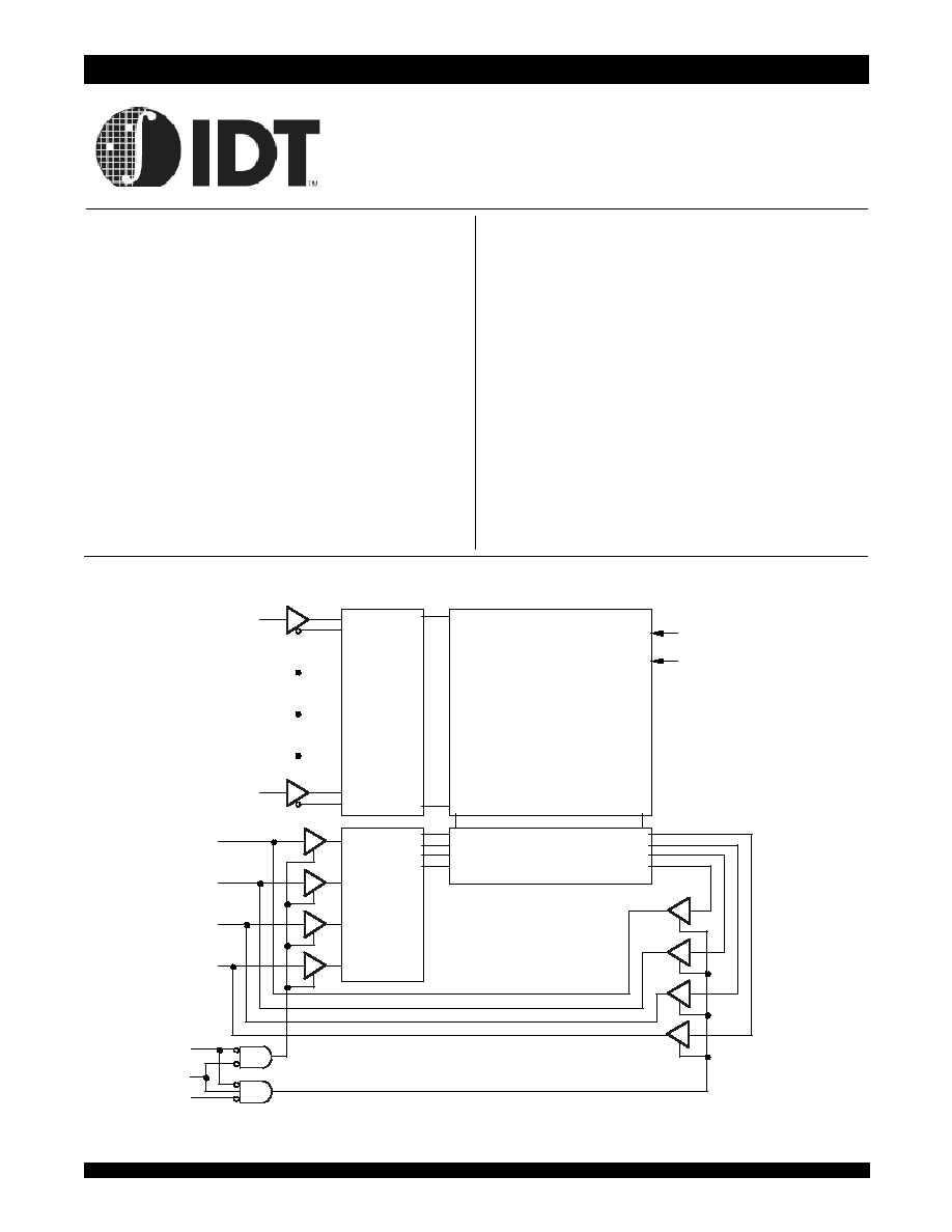
The lDT61298SA is a 262,144-bit high-speed static RAM organized
as 64K x 4. It is fabricated using IDT's high-performance, high-reliability
CMOS technology. This state-of-the-art technology, combined with inno-
vative circuit design techniques, provides a cost-effective approach for
memory intensive applications.
The IDT61298SA features two memory control functions: Chip Select
(
CS) and Output Enable (OE). These two functions greatly enhance the
IDT61298SA's overall flexibility in high-speed memory applications.
Access times as fast as 12ns are available. The IDT61298SA offers
a reduced power standby mode, I
SB1
, which enables the designer to
considerably reduce device power requirements. This capability signifi-
cantly decreases system power and cooling levels, while greatly enhanc-
ing system reliability.
All inputs and outputs are TTL-compatible and the device operates from
a single 5V supply. Fully static asynchronous circuitry, along with matching
access and cycle times, favor the simplified system design approach.
The IDT61298SA is packaged in a 300 mil, 28-pin SOJ, providing
improved board-level packing densities.
Functional Block Diagram
A
0
D
E
C
O
D
E
R
262,144-BIT
MEMORY ARRAY
I/O CONTROL
2971 drw 01
INPUT
DATA
CONTROL
WE
OE
CS
I/O
0
I/O
1
I/O
2
I/O
3
A
15
V
CC
GND
,
CMOS Static RAM
256K (64K x 4-Bit)
IDT61298SA
2
IDT61298SA
CMOS Static RAM 256K (64K x 4-Bit) Commercial Temperature Range
2971 drw 02
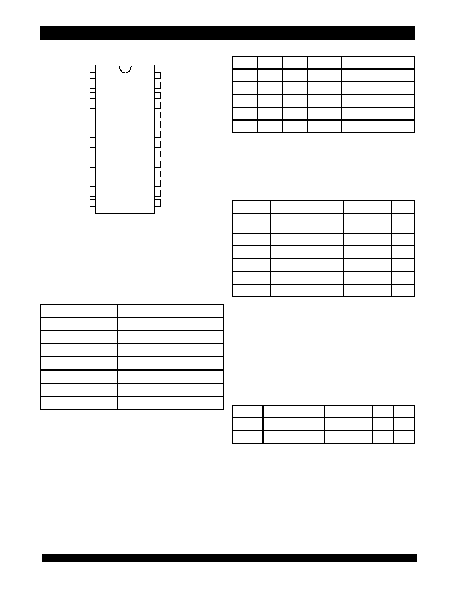
5
6
7
8
9
10
11
12
1
2
3
4
24
23
22
21
20
19
18
17
SO28-5
13
14
28
27
26
25
16
15
NC
A
0
A
1
A
2
A
3
A
4
A
5
A
6
A
7
A
8
A
9
CS
OE
GND
V
CC
A
15
A
14
A
13
A
12
A
11
A
10
NC
NC
I/O
3
I/O
2
I/O
1
I/O
0
WE
,
Absolute Maximum Ratings
(1)
Pin Configuration
SOJ
Top View
Capacitance
(T
A
= +25∞C, f = 1.0MHz, SOJ Package)
Truth Table
(1,2)
Pin Descriptions
Name
Description
A
0
- A
14
Addresses
I/O
0
- I/O
7
Data Input/Output
CS
Chip Select
WE
Write Enable
OE
Output Enable
GND
Ground
V
CC
Power
2971 tbl 01
NOTES:
1. H = V
IH
, L = V
IL
, x = Don't care.
2. V
LC
= 0.2V, V
HC
= V
CC
-0.2V.
3. Other inputs
V
HC
or
V
LC
.
CS
OE
WE
I/O
Function
L
L
H
DATA
OUT
Read Data
L
X
L
DATA
IN
Write Data
L
H
H
High-Z
Outputs Disabled
H
X
X
High-Z
Deselecte d - Standby (I
SB
)
V
HC
(3)
X
X
High-Z
Deselecte d - Standby (I
SB1
)
2971 tbl 02
NOTES:
1. Stresses greater than those listed under ABSOLUTE MAXIMUM RATINGS
may cause permanent damage to the device. This is a stress rating only and
functional operation of the device at these or any other conditions above those
indicated in the operational sections of this specification is not implied. Exposure
to absolute maximum rating conditions for extended periods may affect
reliability.
2. V
TERM
must not exceed V
CC
+ 0.5V.
Symbol
Rating
Com'l.
Unit
V
TERM
(2)
Terminal Voltage
with Respect to GND
-0.5 to +7.0
V
T
A
Operating Temperature
0 to +70
o
C
T
BIAS
Temperature Under Bias
-55 to +125
o
C
T
STG
Storage Temperature
-55 to +125
o
C
P
T
Power Dissipation
1.0
W
I
OUT
DC Output Current
50
mA
2971 tbl 03
NOTE:
1. This parameter is determined by device characterization, but is not production
tested.
Symbol
Parameter
(1)
Conditions
Max.
Unit
C
IN
Input Capacitance
V
IN
= 3dV
5
pF
C
OUT
Output Capacitance
V
OUT
= 3dV
7
pF
2971 tbl 04
6.42
IDT61298SA
CMOS Static RAM 256K (64K x 4-Bit) Commercial Temperature Range
3
Recommended DC Operating
Conditions
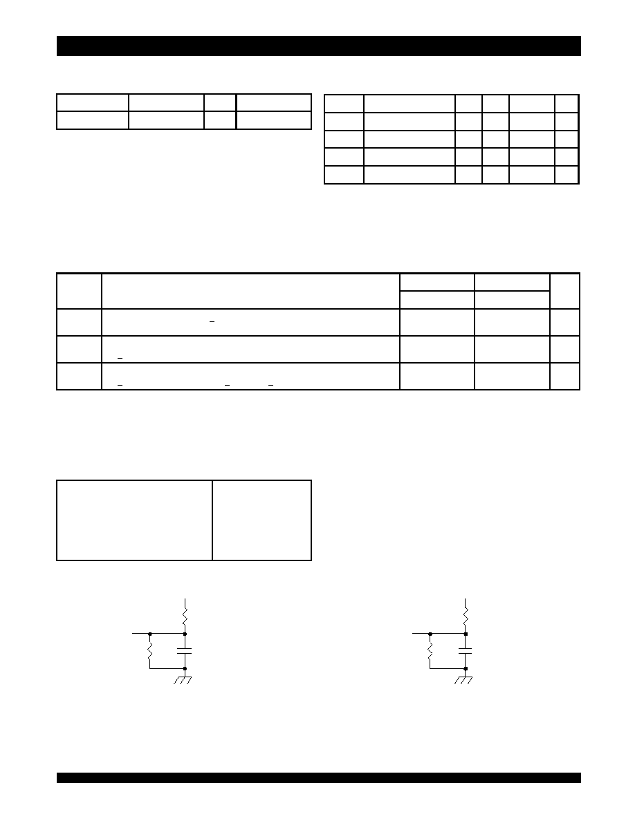
Figure 1. AC Test Load
Figure 2. AC Test Load
(for t
CLZ
, t
OLZ
, t
CHZ
, t
OHZ
, t
OW
, t
WHZ
)
AC Test Conditions
*Includes scope and jig capacitances
Recommended Operating
Temperature and Supply Voltage
DC Electrical Characteristics
(1)
(V
CC
= 5V ± 10%, V
LC
= 0.2V, V
HC
= V
CC
- 0.2V)
2971 drw 03
480
30pF*
255
DATA
OUT
5V
,
2971 drw 04
480
5pF*
255
DATA
OUT
5V
,
Grade
Temperature
GND
Vcc
Commercial
0
O
C to +70
O
C
0V
5V ± 10%
2971 tbl 05
NOTE:
1. V
IL
(min.) = ≠1.5V for pulse width less than 10ns, once per cycle.
Symbol
Parameter
Min.
Typ.
Max.
Unit
V
CC
Supply Voltage
4.5
5.0
5.5
V
GND
Ground
0
0
0
V
V
IH
Input High Voltage
2.2
____
V
CC
+ 0.5V
V
V
IL
Input Low Voltage
-0.5
(1)
____
0.8
V
2971 tbl 06
NOTES:
1. All values are maximum guaranteed values.
2. f
MAX
= 1/t
RC
(all address inputs are cycling at f
MAX
); f = 0 means no address input lines are changing.
Symbol
Parameter
61298SA12
61298SA15
Unit
Com'l.
Com'l.
I
CC
Dynamic Operating Current
CS < V
IL
, Outputs
Open, V
CC
= Max., f = f
MAX
(2)
160
140
mA
I
SB
Standby Power Supply Current (TTL Level)
CS > V
IH
, V
CC
= Max., Outputs Open, f = f
MAX
(2)
50
45
mA
I
SB1
Full Standby Power Supply Current (CMOS Level)
CS > V
HC
, V
CC
= Max., f = 0
(2)
, V
IN
< V
LC
or V
IN
> V
HC
20
20
mA
2971 tbl 07
Input Pulse Levels
Input Rise/Fall Times
Input Timing Reference Levels
Output Reference Levels
AC Test Load
GND to 3.0V
3ns
1.5V
1.5V
See Figures 1 and 2
2971 tbl 08
4
IDT61298SA
CMOS Static RAM 256K (64K x 4-Bit) Commercial Temperature Range
DC Electrical Characteristics
(V
CC
= 5.0V ± 10%)
AC Electrical Characteristics
(V
CC
= 5.0V ± 10%)
Symbol
Parameter
Test Conditions
IDT61298SA
Unit
Min.
Typ.
Max.
|I
LI
|
Input Leakage Current
V
CC
= Max., V
IN
=
GND to V
CC
____
____
5
µ A
|I
LO
|
Output Leakage Current
V
CC
= Max.,
CS = V
IH
, V
OUT
= GND to V
CC
____
____
5
µ A
V
OL
Output Low Voltage
I
OL
= 8mA, V
CC
= Min.
I
OL
= 10mA, V
CC
= Min.
____
____
____
____
0.4
0.5
V
V
OH
Output High Voltage
I
OH
= -4mA, V
CC
= Min.
2.4
___
___
V
2971 tbl 09
NOTE:
1. This parameter is guaranteed with AC test load (Figure 2) by device characterization, but is not production tested.
Symbol
Parameter
61298SA12
61298SA15
Unit
Min.
Max.
Min.
Max.
Read Cycle
t
RC
Read Cycle Time
12
____
15
____
ns
t
AA
Address Access Time
____
12
____
15
ns
t
ACS
Chip Select Access Time
____
12
____
15
ns
t
CLZ
(1)
Chip Select to Output in Low-Z
4
____
4
____
ns
t
CHZ
(1)
Chip Desele ct to Output in High-Z
____
6
____
7
ns
t
OE
Output Enable to Output Valid
____
6
____
7
ns
t
OLZ
(1)
Output Enab le to Output in Low-Z
0
____
0
____
ns
t
OHZ
(1)
Output Disab le to Output in High-Z
____
6
____
6
ns
t
OH
Output Hold from Address Change
3
____
3
____
ns
t
PU
(1)
Chip Select to Power-Up Time
0
____
0
____
ns
t
PD
(1)
Chip Deselect to Power-Down Time
____
12
____
15
ns
Write Cycle
t
WC
Write Cycle Time
12
____
15
____
ns
t
CW
Chip Select to End-of-Write
9
____
10
____
ns
t
AW
Address Valid to End-of-Write
9
____
10
____
ns
t
AS
Address Set-up Time
0
____
0
____
ns
t
WP
Write Pulse Width
9
____
10
____
ns
t
WR
Write Recovery Time
0
____
0
____
ns
t
DW
Data Valid to End-of-Write
6
____
7
____
ns
t
DH
Data Hold Time
0
____
0
____
ns
t
WHZ
(1)
Write Enab le to Output in High-Z
____
6
____
6
ns
t
OW
(1)
Output Active from End-of-Write
4
____
4
____
ns
2971 tbl 10
6.42
IDT61298SA
CMOS Static RAM 256K (64K x 4-Bit) Commercial Temperature Range
5
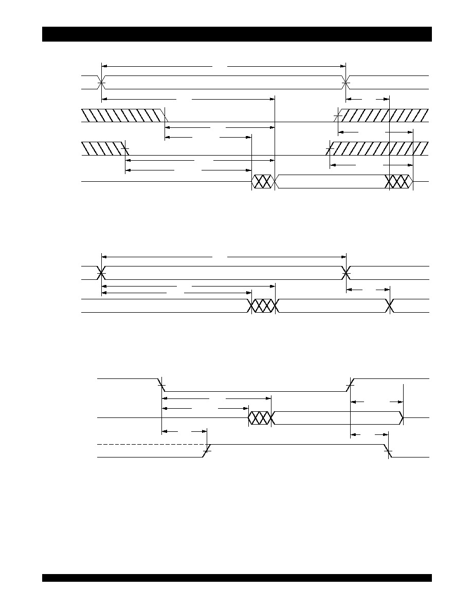
Timing Waveform of Read Cycle No. 1
(1)
Timing Waveform of Read Cycle No. 3
(1,3,4)
NOTES:
1.
WE is HIGH for Read cycle.
2. Device is continuously selected,
CS is LOW.
3. Address valid prior to or coincident with
CS transition LOW.
4.
OE is LOW.
5. Transition is measured ±200mV from steady state.
Timing Waveform of Read Cycle No. 2
(1,2,4)
2971 drw 06
ADDRESS
DATA
t
RC
t
AA
t
OH
OUT
t
OH
DATA VALID
,
2971 drw 05
ADDRESS
CS
OE
DATA
t
RC
t
AA
t
OH
t
OHZ
t
OE
OUT
t
ACS
t
CLZ
(5)
t
CHZ
t
OLZ
(5)
(5)
(5)
DATA VALID
,
2971 drw 07
DATA
OUT
CS
t
ACS
(5)
t
CLZ
CHZ
t
t
PD
t
PU
I
CC
I
SB
SUPPLY
CURRENT
V
CC
(5)
DATA VALID
,