 | –≠–ª–µ–∫—Ç—Ä–æ–Ω–Ω—ã–π –∫–æ–º–ø–æ–Ω–µ–Ω—Ç: 70121 | –°–∫–∞—á–∞—Ç—å:  PDF PDF  ZIP ZIP |
©1998 Integrated Device Technology, Inc.
JUNE 1999
DSC 2654/8
1
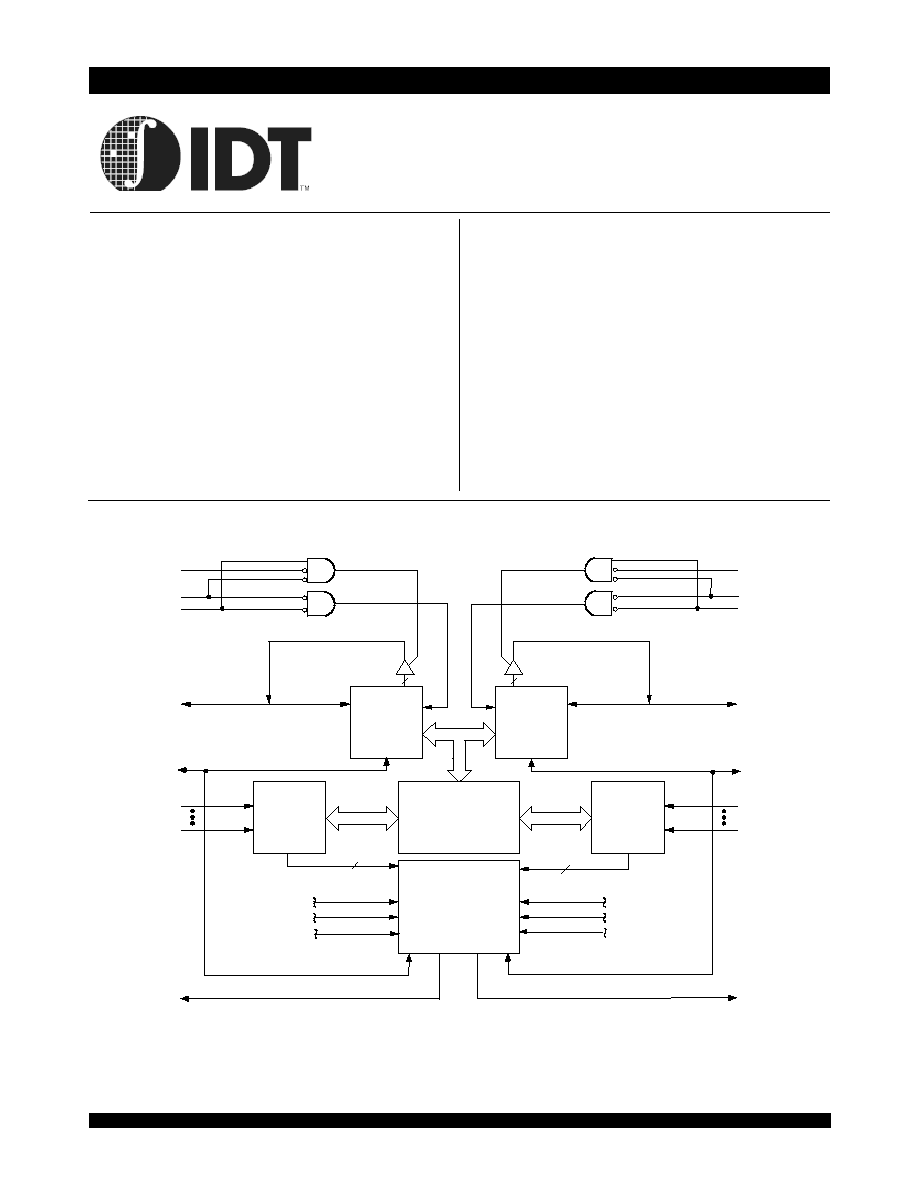
I/O
Control
Address
Decoder
MEMORY
ARRAY
ARBITRATION
INTERRUPT
LOGIC
Address
Decoder
I/O
Control
R/
W
L
CE
L
OE
L
BUSY
L
A
10L
A
0L
2654 drw 01
I/O
0L
- I/O
8L
CE
L
OE
L
R/
W
L
INT
L
BUSY
R
I/O
0R
-I/O
8R
A
10R
A
0R
INT
R
CE
R
OE
R
(2)
(1,2)
(1,2)
(2)
R/
W
R
CE
R
OE
R
R/
W
R
11
11
HIGH-SPEED
2K x 9 DUAL-PORT
STATIC RAM
WITH BUSY & INTERRUPT
IDT70121S/L
IDT70125S/L
NOTES:
1. 70121 (MASTER): BUSY is non-tri-stated push-pull output.
70125 (SLAVE): BUSY is input.
2. INT is totem-pole output.
Functional Block Diagram
Features
x
High-speed access
Commercial: 25/35/45/55ns (max.)
x
Low-power operation
IDT70121/70125S
Active: 675mW (typ.)
Standby: 5mW (typ.)
IDT70121/70125L
Active: 675mW (typ.)
Standby: 1mW (typ.)
x
Fully asychronous operation from either port
x
MASTER IDT70121 easily expands data bus width to 18 bits or more
using SLAVE IDT70125 chip
x
On-chip port arbitration logic (IDT70121 only)
x
BUSY
output flag on Master; BUSY input on Slave
x
INT
flag for port-to-port communication
x
Battery backup operation2V data retention
x
TTL-compatible, signal 5V (±10%) power supply
x
Available in 52-pin PLCC
x
Industrial temperature range (40∞C to +85∞C) is available for
selected speeds
Description
The IDT70121/IDT70125 are high-speed 2K x 9 Dual-Port Static
RAMs. The IDT70121 is designed to be used as a stand-alone 9-bit Dual-
Port RAM or as a MASTER Dual-Port RAM together with the IDT70125
SLAVE Dual-Port in 18-bit-or-more word width systems. Using the IDT
MASTER/SLAVE Dual-Port RAM approach in 18-bit-or-wider memory
system applications results in full-speed, error-free operation without the
need for additional discrete logic.

6.42
IDT70121/IDT70125
High-Speed 2K x 9 Dual-Port Static RAM with Busy & Interrupt Industrial and Commercial Temperature Ranges
2
A
9R
G
N
D
2
1
2
2
2
3
2
4
2
5
2
6
2
7
2
8
2
9
3
0
3
1
3
2
7
6
5
4
3
2
5
2
5
1
5
0
4
9
4
8
4
7
3
3
8
9
10
11
12
13
14
15
16
17
18
IDT70121/125J
J52-1
(4)
19
A
6L
A
7L
A
1L
A
2L
A
3L
A
4L
A
5L
A
8L
I/O
0L
I/O
1L
I/O
2L
I/O
3L
46
45
44
43
42
41
40
39
38
37
36
35
A
5R
A
6R
A
0R
A
1R
A
2R
A
3R
A
4R
A
7R
A
8R
I/O
8R
I/O
7R
1
INDEX
34
20
OE
R
A
9L
2654 drw 02
52-Pin PLCC
Top View
(5)
A
1
0
R
I
N
T
R
R
/
W
R
C
E
R
V
C
C
C
E
L
I
N
T
L
A
1
0
L
O
E
L
A
0
L
I
/
O
4
L
I
/
O
5
L
I
/
O
6
L
I
/
O
7
L
I
/
O
8
L
I
/
O
0
R
I
/
O
1
R
I
/
O
2
R
I
/
O
3
R
I
/
O
4
R
I
/
O
5
R
I
/
O
6
R
B
U
S
Y
R
R
/
W
L
B
U
S
Y
L
Description (con't.)
Pin Configurations
(1,2,3)
Both devices provide two independent ports with separate control,
address, and I/O pins that permit independent, asynchronous access for
reads or writes to any location in memory. An automatic power-down
feature, controlled by CE, permits the on-chip circuitry of each port to enter
a very low standby power mode.
The IDT70121/IDT70125 utilizes a 9-bit wide data path to allow for
Data/Control and parity bits at the users option. This feature is especially
useful in data communications applications where it is necessary to use a
parity bit for transmission/reception error checking.
Fabricated using IDTs CMOS high-performance technology, these
devices typically operate on only 675mW of power. Low-power (L)
versions offer battery backup data retention capability with each port
typically consuming 200µW from a 2V battery.
The IDT70121/IDT70125 devices are packaged in a 52-pin PLCC.
NOTES:
1. All V
CC
pins must be connected to power supply.
2. All GND pins must be connected to ground supply.
3. Package body is approximately .75 in x .75 in x .17 in.
4. This package code is used to reference the package diagram.
5. This text does not indicate orientation of the actual part-marking.
3
IDT70121/IDT70125
High-Speed 2K x 9 Dual-Port Static RAM with Busy & Interrupt Industrial and Commercial Temperature Ranges
Maximum Operating Temperature
and Supply Voltage
(1,2)
Recommended DC
Operating Conditions
Absolute Maximum Ratings
(1)
Capacitance
(T
A
= +25∞C, f = 1.0MHz)
NOTES:
1. Stresses greater than those listed under ABSOLUTE MAXIMUM RATINGS may
cause permanent damage to the device. This is a stress rating only and functional
operation of the device at these or any other conditions above those indicated
in the operational sections of this specification is not implied. Exposure to absolute
maximum rating conditions for extended periods may affect reliabilty.
2. V
TERM
must not exceed Vcc + 10% for more than 25% of the cycle time or 10ns
maximum, and is limited to < 20mA for the period of V
TERM
> V
cc
+ 10%.
NOTES:
1. V
IL
> -1.5V for pulse width less than 10ns.
2. V
TERM
must not exceed Vcc + 10%.
NOTES:
1. This is the parameter T
A
.
2. Industrial temperature: for specific speeds, packages and powers contact your
sales office.
NOTE:
1. This parameter is determined by device characterization but is not production
tested.
DC Electrical Characteristics Over the Operating
Temperature and Supply Voltage Range
(V
CC
= 5.0V ± 10%)
NOTE:
1. At Vcc < 2.0V leakages are undefined.
Symbol
Rating
Commercial
& Industrial
Unit
V
TERM
(2)
Terminal Voltage
with Respect
to GND
-0.5 to +7.0
V
T
BIAS
Temperature
Under Bias
-55 to +125
o
C
T
STG
Storage
Temperature
-55 to +125
o
C
I
OUT
DC Output
Current
50
mA
2654 tbl 01
Grade
Ambient
Temperature
GND
Vcc
Commercial
0
O
C to +70
O
C
0V
5.0V
+
10%
Industrial
-40
O
C to +85
O
C
0V
5.0V
+
10%
2654 tbl 02
Symbol
Parameter
Min.
Typ.
Max.
Unit
V
CC
Supply Voltage
4.5
5.0
5.5
V
GND
Ground
0
0
0
V
V
IH
Input High Voltage
2.2
____
6.0
(2)
V
V
IL
Input Low Voltage
-0.5
(1)
____
0.8
V
2654 tbl 03
Symbol
Parameter
Conditions
(1)
Max. Unit
C
IN
Input Capacitance
V
IN
= 3dV
9
pF
C
OUT
Output Capacitance
V
OUT
= 3dV
10
pF
2654 tbl 04
Symbol
Parameter
Test Conditions
70121S
70125S
70121L
70125L
Unit
Min.
Max.
Min.
Max.
|I
LI
|
Input Leakage Current
(1)
V
CC
= 5.5V, V
IN
= 0V to V
CC
___
10
___
5
µA
|I
LO
|
Output Leakage Current
V
CC
= 5.5V, CE = V
IH
, V
OUT
= 0V to V
CC
___
10
___
5
µA
V
OL
Output Low Voltage
I
OL
= +4mA
___
0.4
___
0.4
V
V
OH
Output High Voltage
I
OH
= -4mA
2.4
___
2.4
___
V
2654 tbl 05

6.42
IDT70121/IDT70125
High-Speed 2K x 9 Dual-Port Static RAM with Busy & Interrupt Industrial and Commercial Temperature Ranges
4
DC Electrical Characteristics Over the Operating
Temperature and Supply Voltage Range
(1,4,6)
(V
CC
= 5V ± 10%)
NOTES:
1. 'X' in part numbers indicates power rating (S or L).
2. At f = f
MAX
, address and control lines (except Output Enable) are cycling at the maximum frequency read cycle of 1/t
RC
, and using AC TEST CONDITIONS of
input levels of GND to 3V.
3. f = 0 means no address or control lines change. Applies only to inputs at CMOS level standby.
4. Vcc=5V, T
A
=+25∞C for Typ, and is not production tested.
5. Port "A" may be either left or right port. Port "B" is opposite from port "A".
6. Industrial temperature: for specific speeds, packages and powers contact your sales office.
70121X25
70125X25
Com'l Only
70121X35
70125X35
Com'l Only
Symbol
Parameter
Test Condition
Version
Typ.
Max.
Typ.
Max.
Unit
I
CC
Dynamic Operating Current
(Both Ports Active)
CE
= V
IL
, Outputs Open
f = f
MAX
COM'L
S
L
135
135
260
220
135
135
250
210
mA
IND
S
L
135
135
285
260
135
135
275
250
I
SB1
Standby Current
(Both Ports - TTL Level Inputs)
CE
"A"
= CE
"B"
= V
IH
f = f
MAX
COM'L
S
L
30
30
65
45
30
30
65
45
mA
IND
S
L
30
30
80
65
30
30
80
65
I
SB2
Standby Current
(One Port - TTL Level Inputs)
CE
"A"
= V
IL
and CE
"B"
= V
IH
#
Active Port Outputs Open,
f=f
MAX
COM'L
S
L
80
80
175
145
80
80
165
135
mA
IND
S
L
80
80
200
175
80
80
190
165
I
SB3
Full Standby Current (Both Ports
- CMOS Level Inputs)
CE
"A"
and CE
"B"
> V
CC
- 0.2V
V
IN
> V
CC
- 0.2V or
VIN < 0.2V, f = 0
!
COM'L
S
L
1.0
0.2
15
5
1.0
0.2
15
5
mA
IND
S
L
1.0
0.2
15
5
1.0
0.2
15
5
I
SB4
Full Standby Current
(One Port - CMOS Level Inputs)
CE
"A"
< 0.2V and
CE
"B"
> V
CC
- 0.2V
#
V
IN
> V
CC
- 0.2V or V
IN
< 0.2V
Active Port Outputs Open
f = f
MAX
COM'L
S
L
70
70
170
140
70
70
160
130
mA
IND
S
L
70
70
195
170
70
70
185
160
2654 tbl 06a
70121X45
70125X45
Com'l Only
70121X55
70125X55
Com'l Only
Symbol
Parameter
Test Condition
Version
Typ.
Max.
Typ.
Max.
Unit
I
CC
Dynamic Operating Current
(Both Ports Active)
CE
= V
IL
, Outputs Open
f = f
MAX
COM'L
S
L
135
135
245
205
135
135
240
200
mA
IND
S
L
135
135
270
245
135
135
265
240
I
SB1
Standby Current
(Both Ports - TTL Level Inputs)
CE
"A"
= CE
"B"
= V
IH
f = f
MAX
COM'L
S
L
30
30
65
45
30
30
65
45
mA
IND
S
L
30
30
80
65
30
30
80
65
I
SB2
Standby Current
(One Port - TTL Level Inputs)
CE
"A"
= V
IL
and CE
"B"
= V
IH
#
Active Port Outputs Open,
f=f
MAX
COM'L
S
L
80
80
160
130
80
80
155
125
mA
IND
S
L
80
80
185
160
80
80
180
155
I
SB3
Full Standby Current
(Both Ports - CMOS Level
Inputs)
CE
"A"
and CE
"B"
> V
CC
- 0.2V
V
IN
> V
CC
- 0.2V or
V
IN
< 0.2V, f = 0
!
COM'L
S
L
1.0
0.2
15
5
1.0
0.2
15
5
mA
IND
S
L
1.0
0.2
15
5
1.0
0.2
15
5
I
SB4
Full Standby Current
(One Port - CMOS Level Inputs)
CE
"A"
< 0.2V and
CE
"B"
> V
CC
- 0.2V
#
V
IN
> V
CC
- 0.2V or V
IN
< 0.2V
Active Port Outputs Open
f = f
MAX
COM'L
S
L
70
70
155
125
70
70
150
120
mA
IND
S
L
70
70
180
155
70
70
175
150
2654 tbl 06b
5
IDT70121/IDT70125
High-Speed 2K x 9 Dual-Port Static RAM with Busy & Interrupt Industrial and Commercial Temperature Ranges
Data Retention Characteristics
(L Version Only)
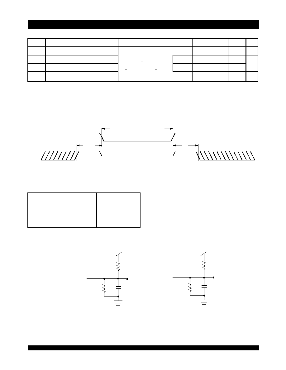
Data Retention Waveform
AC Test Conditions
Figure 1. AC Output Test Load
Figure 2. Output Test Load
(For t
LZ
, t
HZ
, t
WZ
, t
OW
)
*Including scope and jig.
NOTES:
1. V
CC
= 2V, T
A
= +25∞C, and are not production tested.
2. t
RC
= Read Cycle Time.
3. This parameter is guaranteed but is not production tested.
V
DR
2V
DATA RETENTION MODE
Vcc
CE
4.5V
t
CDR
t
R
V
IH
V
DR
V
IH
4.5V
2654 drw 03
1250
30pF
775
DATA
OUT
BUSY
INT
5V
5V
1250
5pF*
775
DATA
OUT
2654 drw 04
Symbol
Parameter
Test Condition
Min.
Typ.
(1)
Max.
Unit
V
DR
V
CC
for Data Retention
2.0
___
___
V
I
CCDR
Data Retention Current
V
CC
= 2V, CE > V
CC
- 0.2V
IND.
___
100
4000
µA
t
CDR
(3)
Chip Deselect to Data Retention Time
V
IN
> V
CC
- 0.2V or V
IN
< 0.2
COM'L.
___
100
1500
t
R
(3)
Operation Recovery Time
t
RC
(2)
___
___
V
2654 tbl 07
Input Pulse Levels
Input Rise/Fall Times
Input Timing Reference Levels
Output Reference Levels
Output Load
GND to 3.0V
5ns
1.5V
1.5V
Figures 1 and 2
2654 tbl 08