 | –≠–ª–µ–∫—Ç—Ä–æ–Ω–Ω—ã–π –∫–æ–º–ø–æ–Ω–µ–Ω—Ç: 7035 | –°–∫–∞—á–∞—Ç—å:  PDF PDF  ZIP ZIP |
©1999 Integrated Device Technology, Inc.
SEPTEMBER 1999
DSC 4088/5
1
I/O
Control
Address
Decoder
MEMORY
ARRAY
ARBITRATION
INTERRUPT
SEMAPHORE
LOGIC
Address
Decoder
I/O
Control
R/
W
L
BUSY
L
A
12L
A
0L
4088 drw 01
UB
L
LB
L
CE
L
OE
L
I/O
9L
-I/O
17L
I/O
0L
-I/O
8L
CE
L
OE
L
R/
W
L
SEM
L
INT
L
M/
S
R/
W
R
BUSY
R
UB
R
LB
R
CE
R
OE
R
I/O
9R
-I/O
17R
I/O
0R
-I/O
8R
A
12R
A
0R
R/
W
R
SEM
R
INT
R
CE
R
OE
R
(2)
(1,2)
(1,2)
(2)
13
13
IDT7035S/L
HIGH-SPEED
8K x 18 DUAL-PORT
STATIC RAM
Features
x
x
x
x
x
True Dual-Ported memory cells which allow simultaneous
reads of the same memory location
x
x
x
x
x
High-speed access
Commercial: 15/20ns (max.)
x
x
x
x
x
Low-power operation
IDT7035S
Active: 800mW (typ.)
Standby: 5mW (typ.)
IDT7035L
Active: 800mW (typ.)
Standby: 1mW (typ.)
x
x
x
x
x
Separate upper-byte and lower-byte control for multiplexed
bus compatibility
x
x
x
x
x
IDT7035 easily expands data bus width to 36 bits or more
using the Master/Slave select when cascading more than
one device
x
x
x
x
x
M/S = H for BUSY output flag on Master
M/S = L for BUSY input on Slave
x
x
x
x
x
Interrupt Flag
x
x
x
x
x
On-chip port arbitration logic
x
x
x
x
x
Full on-chip hardware support of semaphore signaling
between ports
x
x
x
x
x
Fully asynchronous operation from either port
x
x
x
x
x
Battery backup operation2V data retention
x
x
x
x
x
TTL-compatible, single 5V (±10%) power supply
x
x
x
x
x
Available in 100-pin Thin Quad Flatpack
Industrial temperature range (40∞C to +85∞C) is available
for selected speeds
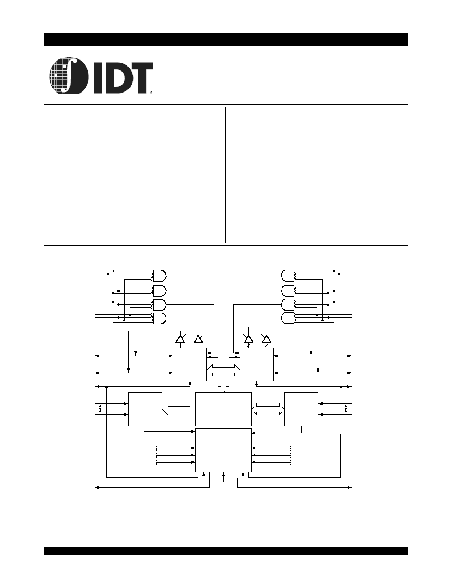
Functional Block Diagram
NOTES:
1. (MASTER): BUSY is output; (SLAVE): BUSY is input.
2. BUSY outputs and INT outputs are non-tri-stated push-pull.
6.42
IDT7035S/L
High-Speed 8K x 18 Dual-Port Static RAM Industrial and Commercial Temperature Ranges
2
Description
The IDT7035 is a high-speed 8K x 18 Dual-Port Static RAM. The
IDT7035 is designed to be used as a stand-alone 144K-bit Dual-Port RAM
or as a combination MASTER/SLAVE Dual-Port RAM for 36-bit or more
word systems. Using the IDT MASTER/SLAVE Dual-Port RAM approach
in 36-bit or wider memory system applications results in full-speed, error-
free operation without the need for additional discrete logic.
This device provides two independent ports with separate control,
address, and I/O pins that permit independent, asynchronous access for
reads or writes to any location in memory. An automatic power down
feature controlled by Chip Enable (CE) permits the on-chip circuitry of each
port to enter a very low standby power mode.
The IDT7035 utilizes a 18-bit wide data path to alow for parity at the
user's option. This feature is especially useful in data communications
applications where it is necessary to use a parity bit for transmission/
reception error checking.
Fabricated using IDTs CMOS high-performance technology, these
devices typically operate on only 800mW of power. Low-power (L)
versions offer battery backup data retention capability with typical power
consumption of 500µW from a 2V battery.
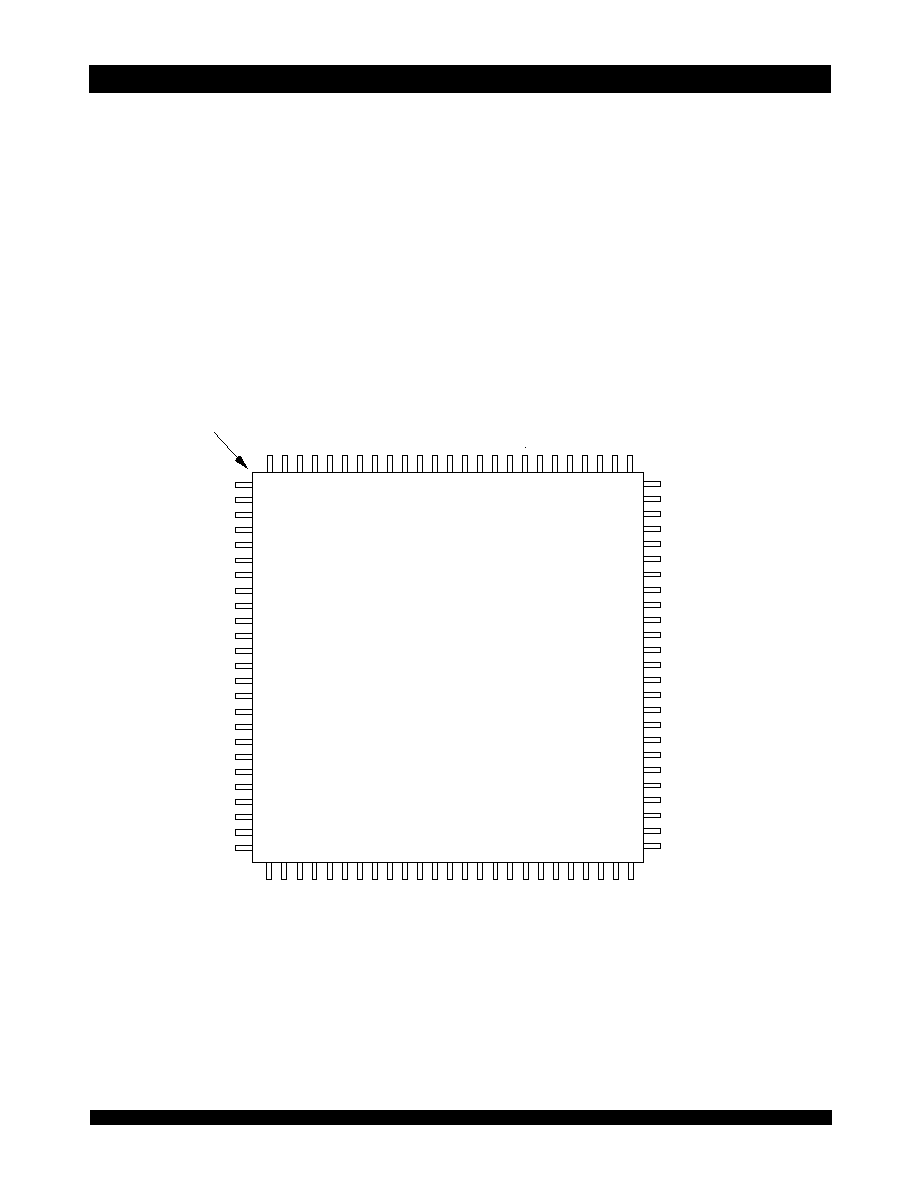
Pin Configurations
(1,2,3)
NOTES:
1. All V
CC
pins must be connected to power supply.
2. All GND pins must be connected to ground supply.
3. Package body is approximately 14mm x 14mm x 1.4mm.
4. This package code is used to reference the package diagram.
5. This text does not indicate orientation of the actual part-marking.
Index
1
2
3
4
5
6
7
8
9
10
11
12
13
14
15
16
17
18
19
20
21
22
23
24
25
75
74
73
72
71
70
69
68
67
66
65
64
63
62
61
60
59
58
57
56
55
54
53
52
51
26 27 28 29 30 31 32 33 34 35 36 37 38 39 40 41 42 43 44 45 46 47 48 49 50
100 99 98 97 96 95 94 93 92 91 90 89 88 87 86 85 84 83 82 81 80 79 78 77 76
IDT7035PF
PN100-1
(4)
100-Pin TQFP
Top View
(5)
N/C
N/C
I/O
8L
I/O
17L
I/O
11L
I/O
12L
I/O
13L
I/O
14L
GND
I/O
15L
I/O
16L
V
CC
GND
I/O
0R
I/O
1R
I/O
2R
I/O
3R
V
CC
I/O
4R
I/O
5R
I/O
6R
I/O
8R
I/O
17R
N/C
N/C
4088 drw 02
N/C
N/C
N/C
N/C
A
5L
A
4L
A
3L
A
2L
A
1L
A
0L
INT
L
GND
M/
S
BUSY
R
INT
R
A
0R
N/C
N/C
N/C
N/C
BUSY
L
A
1R
A
2R
A
3R
A
4R
I
/
O
1
0
L
I
/
O
9
L
I
/
O
7
L
I
/
O
6
L
I
/
O
5
L
I
/
O
4
L
I
/
O
3
L
I
/
O
2
L
G
N
D
I
/
O
1
L
I
/
O
0
L
O
E
L
V
C
C
R
/
W
L
S
E
M
L
C
E
L
U
B
L
L
B
L
A
1
1
L
A
1
0
L
A
9
L
A
8
L
A
7
L
A
6
L
I
/
O
7
R
I
/
O
9
R
I
/
O
1
0
R
I
/
O
1
1
R
I
/
O
1
2
R
I
/
O
1
3
R
I
/
O
1
4
R
I
/
O
1
5
R
G
N
D
I
/
O
1
6
R
O
E
R
R
/
W
R
S
E
M
R
C
E
R
U
B
R
L
B
R
G
N
D
A
1
1
R
A
1
0
R
A
9
R
A
8
R
A
7
R
A
6
R
A
5
R
A
1
2
L
A
1
2
R
.
6.42
IDT7035S/L
High-Speed 8K x 18 Dual-Port Static RAM Industrial and Commercial Temperature Ranges
3
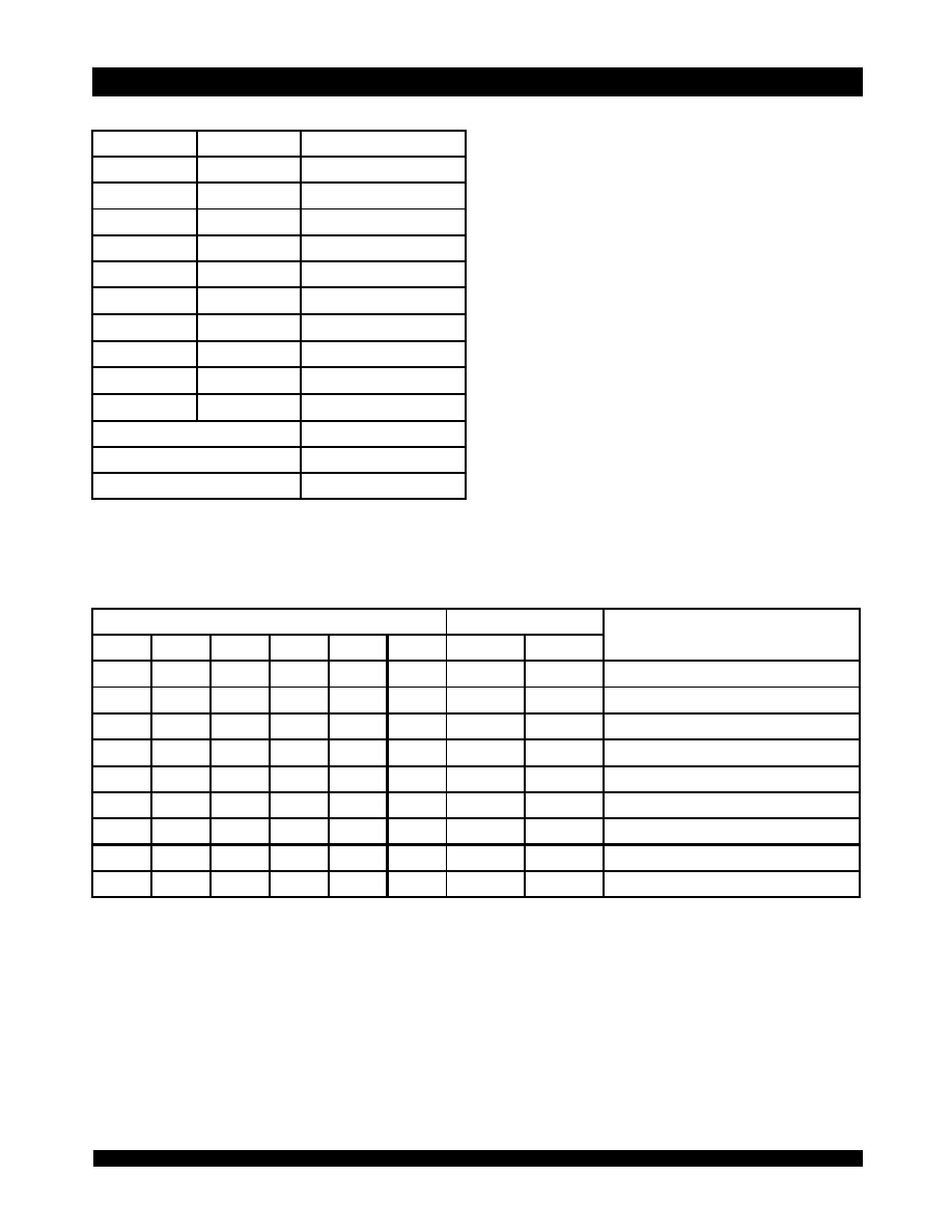
Pin Names
Truth Table I: Non-Contention Read/Write Control
NOTE:
1. A
0L
A
12L
A
0R
A
12R
Left Port
Right Port
Names
CE
L
CE
R
Chip Enable
R/W
L
R/W
R
Read/Write Enable
OE
L
OE
R
Output Enable
A
0L
- A
12L
A
0R
- A
12R
Address
I/O
0L
- I/O
17L
I/O
0R
- I/O
17R
Data Input/Output
SEM
L
SEM
R
Semaphore Enable
UB
L
UB
R
Upper Byte Select
LB
L
LB
R
Lower Byte Select
INT
L
INT
R
Interrupt Flag
BUSY
L
BUSY
R
Busy Flag
M/S
Master or Slave Select
V
CC
Power
GND
Ground
4088 tbl 01
Inputs
(1)
Outputs
Mode
CE
R/W
OE
UB
LB
SEM
I/O
9-17
I/O
0-8
H
X
X
X
X
H
High-Z
High-Z
Deselected: Power-Down
X
X
X
H
H
H
High-Z
High-Z
Both Bytes Deselected
L
L
X
L
H
H
DATA
IN
High-Z
Write to Upper Byte Only
L
L
X
H
L
H
High-Z
DATA
IN
Write to Lower Byte Only
L
L
X
L
L
H
DATA
IN
DATA
IN
Write to Both Bytes
L
H
L
L
H
H
DATA
OUT
High-Z
Read Upper Byte Only
L
H
L
H
L
H
High-Z
DATA
OUT
Read Lower Byte Only
L
H
L
L
L
H
DATA
OUT
DATA
OUT
Read Both Bytes
X
X
H
X
X
X
High-Z
High-Z
Outputs Disabled
4088 tbl 02
6.42
IDT7035S/L
High-Speed 8K x 18 Dual-Port Static RAM Industrial and Commercial Temperature Ranges
4
Recommended DC Operating
Conditions
Maximum Operating
Temperature and Supply Voltage
(1,2)
Capacitance
(T
A
= +25∞C, f = 1.0MHz)
(1)
Absolute Maximum Ratings
(1)
NOTE:
1. There are eight semaphore flags written to via I/O
0
and read from I/O
0
- I/O
17.
These eight semaphores are addressed by A
0
- A
2
.
Truth Table II: Semaphore Read/Write Control
(1)
NOTES:
1. Stresses greater than those listed under ABSOLUTE MAXIMUM RATINGS may
cause permanent damage to the device. This is a stress rating only and
functional operation of the device at these or any other conditions above those
indicated in the operational sections of this specification is not implied. Exposure
to absolute maximum rating conditions for extended periods may affect
reliability.
2. V
TERM
must not exceed Vcc + 10% for more than 25% of the cycle time or 10ns
maximum, and is limited to < 20 mA for the period over V
TERM
> Vcc + 10%.
NOTES:
1. This is the parameter T
A
.
2. Industrial temperature: for specific speeds, packages and powers contact your
sales office.
NOTES:
1. V
IL
> -1.5V for pulse width less than 10ns.
2. V
TERM
must not exceed Vcc + 10%.
NOTES:
1. This parameter is determined by device characterization but is not production
tested. For TQFP Package Only.
2. 3dV references the interpolated capacitance when the input and output signals
switch from 0V to 3V or from 3V to 0V.
Inputs
Outputs
Mode
CE
R/W
OE
UB
LB
SEM
I/O
9-17
I/O
0-8
H
H
L
X
X
L
DATA
OUT
DATA
OUT
Read Data in Semaphore Flag
X
H
L
H
H
L
DATA
OUT
DATA
OUT
Read Data in Semaphore Flag
H
X
X
X
L
DATA
IN
DATA
IN
Write I/O
0
into Semaphore Flag
X
X
H
H
L
DATA
IN
DATA
IN
Write I/O
0
into Semaphore Flag
L
X
X
L
X
L
______
______
Not Allowed
L
X
X
X
L
L
______
______
Not Allowed
4088 tbl 03
Symbol
Rating
Commercial
& Industrial
Unit
V
TERM
(2)
Terminal Voltage
with Respect
to GND
-0.5 to +7.0
V
T
BIAS
Temperature
Under Bias
-55 to +125
o
C
T
STG
Storage
Temperature
-55 to +125
o
C
I
OUT
DC Output
Current
50
mA
4088 tbl 04
Grade
Ambient
Temperature
GND
Vcc
Commercial
0
O
C to +70
O
C
0V
5.0V
+
10%
Industrial
-40
O
C to +85
O
C
0V
5.0V
+
10%
4088 tbl 05
Symbol
Parameter
Min.
Typ.
Max.
Unit
V
CC
Supply Voltage
4.5
5.0
5.5
V
GND
Ground
0
0
0
V
V
IH
Input High Voltage
2.2
____
6.0
(2)
V
V
IL
Input Low Voltage
-0.5
(1)
____
0.8
V
4088 tbl 06
Symbol
Parameter
Conditions
(2)
Max. Unit
C
IN
Input Capacitance
V
IN
= 3dV
9
pF
C
OUT
Output
Capacitance
V
OUT
= 3dV
10
pF
4088 tbl 07
6.42
IDT7035S/L
High-Speed 8K x 18 Dual-Port Static RAM Industrial and Commercial Temperature Ranges
5
DC Electrical Characteristics Over the Operating
Temperature and Supply Voltage Range
(V
CC
= 5.0V ± 10%)
NOTE:
1. At Vcc < 2.0V input leakages are undefined.
DC Electrical Characteristics Over the Operating
Temperature and Supply Voltage Range
(1,6)
(V
CC
= 5.0V ± 10%)
NOTES:
1. 'X' in part numbers indicates power rating (S or L)
2. V
CC
= 5V, T
A
= +25∞C, and are not production tested. Icc dc
=
120mA (TYP)
3. At f = f
MAX
,
address and I/O'
S
are cycling at the maximum frequency read cycle of 1/t
RC
, and using AC Test Conditions of input levels of
GND to 3V.
4. f = 0 means no address or control lines change.
5. Port "A" may be either left or right port. Port "B" is the opposite from port "A".
6. Industrial temperature: for specific speeds, packages and powers contact your sales office.
Symbol
Parameter
Test Conditions
7035S
7035L
Unit
Min.
Max.
Min.
Max.
|I
LI
|
Input Leakage Current
(1)
V
CC
= 5.5V, V
IN
= 0V to V
CC
___
10
___
5
µA
|I
LO
|
Output Leakage Current
CE
= V
IH
, V
OUT
= 0V to V
CC
___
10
___
5
µA
V
OL
Output Low Voltage
I
OL
= 4mA
___
0.4
___
0.4
V
V
OH
Output High Voltage
I
OH
= -4mA
2.4
___
2.4
___
V
4088 tbl 08
Symbol
Parameter
Test Condition
Version
7035X15
Com'l Only
Typ.
(2)
Max.
7035X20
Com'l Only
Typ.
(2)
Max.
Unit
I
CC
Dynamic Operating Current
(Both Ports Active)
CE
= V
IL
, Outputs Open
SEM
= V
IH
f = f
MAX
(3)
COM'L
S
L
170
170
310
260
160
160
290
240
mA
IND
S
L
____
____
____
____
160
160
370
320
I
SB1
Standby Current
(Both Ports - TTL Level
Inputs)
CE
L
= CE
R
= V
IH
SEM
R
= SEM
L
= V
IH
f = f
MAX
(3)
COM'L
S
L
20
20
60
50
20
20
60
50
mA
IND
S
L
____
____
____
____
20
20
90
70
I
SB2
Standby Current
(One Port - TTL Level Inputs)
CE
"A"
= V
IL
and CE
"B"
= V
IH
(5)
Active Port Outputs Open,
f=f
MAX
(3)
SEM
R
= SEM
L
= V
IH
COM'L
S
L
105
105
190
160
95
95
180
150
mA
IND
S
L
____
____
____
____
95
95
240
210
I
SB3
Full Standby Current (Both
Ports - All CMOS Level
Inputs)
Both Ports CE
L
and
CE
R
> V
CC
- 0.2V
V
IN
> V
CC
- 0.2V or
V
IN
< 0.2V, f = 0
(4)
SEM
R
= SEM
L
> V
CC
- 0.2V
COM'L
S
L
1.0
0.2
15
5
1.0
0.2
15
5
mA
IND
S
L
____
____
____
____
1.0
0.2
30
10
I
SB4
Full Standby Current
(One Port - All CMOS Level
Inputs)
CE
"A"
< 0.2V and
CE
"B"
> V
CC
- 0.2V
(5)
SEM
R
= SEM
L
> V
CC
- 0.2V
V
IN
> V
CC
- 0.2V or V
IN
< 0.2V
Active Port Outputs Open
f = f
MAX
(3)
COM'L
S
L
100
100
170
140
90
90
155
130
mA
IND
S
L
____
____
____
____
90
90
225
200
4088 tbl 09