 | –≠–ª–µ–∫—Ç—Ä–æ–Ω–Ω—ã–π –∫–æ–º–ø–æ–Ω–µ–Ω—Ç: 7052 | –°–∫–∞—á–∞—Ç—å:  PDF PDF  ZIP ZIP |
©1999 Integrated Device Technology, Inc.
JUNE 1999
DSC 2674/9
1
IDT7052S/L
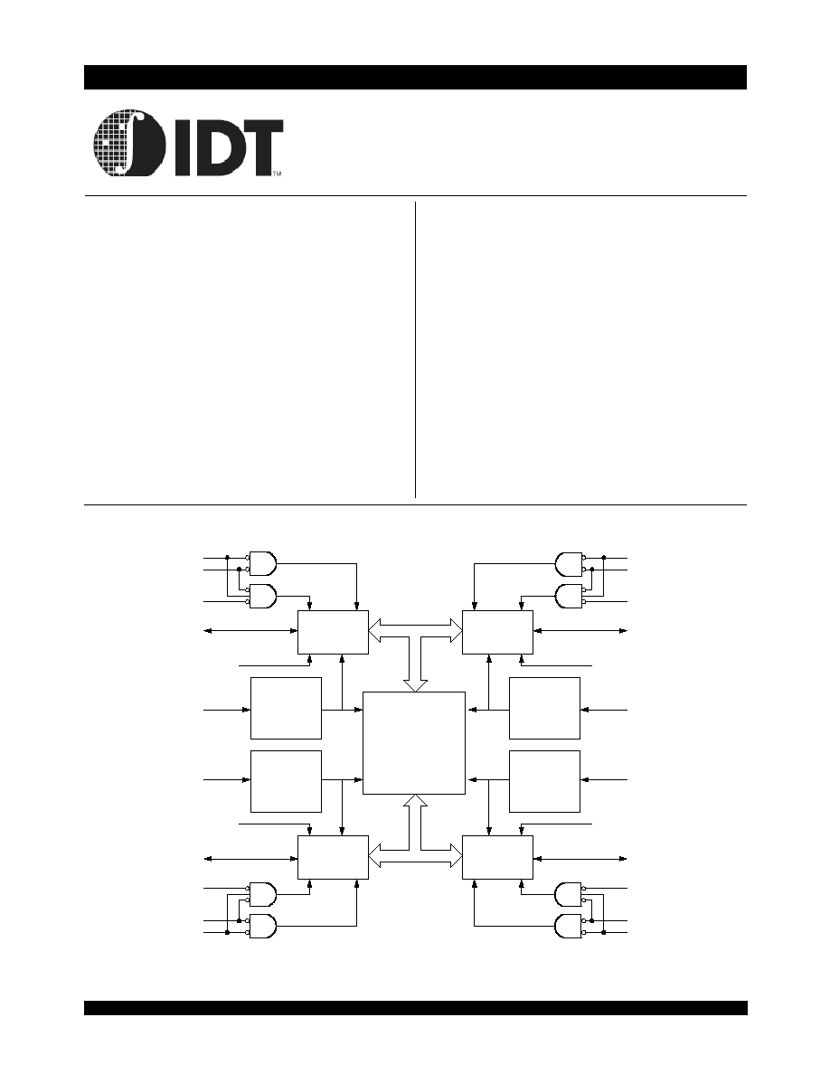
Functional Block Diagram
HIGH-SPEED
2K x 8 FourPort
TM
STATIC RAM
Features
x
x
x
x
x
High-speed access
≠ Military: 25/35ns (max.)
≠ Commercial: 20/25/35ns (max.)
x
x
x
x
x
Low-power operation
≠ IDT7052S
Active: 750mW (typ.)
Standby: 7.5mW (typ.)
≠ IDT7052L
Active: 750mW (typ.)
Standby: 1.5mW (typ.)
x
x
x
x
x
True FourPort memory cells which allow simultaneous
access of the same memory locations
x
x
x
x
x
Fully asynchronous operation from each of the four ports:
P1, P2, P3, P4
x
x
x
x
x
Versatile control for write-inhibit: separate
BUSY input to
control write-inhibit for each of the four ports
x
x
x
x
x
Battery backup operation--2V data retention
MEMORY
ARRAY
COLUMN
I/O
PORT 1
ADDRESS
DECODE
LOGIC
PORT 2
ADDRESS
DECODE
LOGIC
COLUMN
I/O
COLUMN
I/O
PORT 4
ADDRESS
DECODE
LOGIC
PORT 3
ADDRESS
DECODE
LOGIC
COLUMN
I/O
R/
W
P1
I/O
0P1
-I/O
7P1
CE
P1
OE
P1
A
0P1
- A
10P1
BUSY
P2
R/
W
P2
CE
P2
OE
P2
2674 drw 01
I/O
0P2
-I/O
7P2
A
0P2
- A
10P2
BUSY
P1
R/
W
P4
I/O
0P4
-I/O
7P4
CE
P4
OE
P4
A
0P4
- A
10P4
BUSY
P3
R/
W
P3
CE
P3
OE
P3
I/O
0P3
-I/O
7P3
A
0P3
- A
10P3
BUSY
P4
x
x
x
x
x
TTL-compatible; single 5V (±10%) power supply
x
x
x
x
x
Available in 120 pin and 132 pin Thin Quad Flatpacks and
108 pin PGA
x
x
x
x
x
Military product compliant to MIL-PRF-38535 QML
x
x
x
x
x
Industrial temperature range (≠40∞C to +85∞C) is available
for selected speeds
Description
The IDT7052 is a high-speed 2K x 8 FourPortTM Static RAM designed
to be used in systems where multiple access into a common RAM is
required. This FourPort Static RAM offers increased system performance
in multiprocessor systems that have a need to communicate in real time and
also offers added benefit for high-speed systems in which multiple access
is required in the same cycle.
The IDT7052 is also designed to be used in systems where on-chip
hardware port arbitration is not needed. This part lends itself to those

6.42
IDT7052S/L
High-Speed 2K x 8 FourPortTM Static RAM Military, Industrial and Commercial Temperature Ranges
2
NOTES:
1. All V
CC
pins must be connected to the power supply.
2. All GND pins must be connected to the ground supply.
3. Package body is approximately 1.21 in x 1.21 in x .16 in.
4. This package code is used to reference the package diagram.
5. This text does not indicate orientation of the actual part-marking.
Pin Configurations
(1,2,3)
2674 drw 02
OE
P2
A
7
P2
A
8
P2
A
5
P2
80
I/O
2
P1
I/O
3
P1
I/O
6
P1
V
CC
GND
I/O
2
P4
I/O
5
P4
A
3
P2
A
4
P2
A
5
P3
A
7
P3
A
8
P3
OE
P3
A
0
P2
A
1
P3
A
1
P2
A
0
P3
77
74
72
69
68
65
63
60
A
3
P3
A
4
P3
83
78
76
73
70
67
64
61
59
84
56
86
87
88
90
91
92
94
95
97
96
100
99
103
101
105
104
2
1
5
4
7
8
10
12
13
17
16
21
19
25
22
28
24
32
31
34
35
37
39
40
44
43
48
46
52
49
55
51
IDT7052G
G108-1
(4)
108-Pin PGA
Top View
(5)
A
B
C
D
E
F
G
H
J
K
L
M
81
57
54
53
82
79
75
71
66
62
58
50
R/
W
P2
NC
NC
R/
W
P3
BUSY
P2
BUSY
P3
A
6
P2
CE
P3
A
2
P3
A
2
P2
A
6
P3
A
2
P4
A
1
P4
A
9
P3
A
9
P2
CE
A
1
P1
A
2
P1
33
36
38
41
42
45
47
3
6
9
11
14
15
18
20
23
29
30
26
27
85
89
93
98
102
106
107
108
NC
P1
GND
A
5
P1
A
3
P1
A
0
P1
A
6
P1
A
4
P1
V
CC
CE
P1
OE
P1
I/O
0
P1
A
8
P1
A
9
P1
A
7
P1
R/
W
P1
BUSY
I/O
1
P1
V
CC
V
CC
V
CC
GND
I/O
6
P4
I/O
4
P1
I/O
7
P1
I/O
0
P2
I/O
2
P2
I/O
4
P2
I/O
6
P2
I/O
1
P3
I/O
3
P3
I/O
5
P3
I/O
7
P3
I/O
3
P4
I/O
4
P4
I/O
5
P1
NC
I/O
1
P2
I/O
3
P2
I/O
5
P2
I/O
7
P2
I/O
0
P3
I/O
2
P3
I/O
4
P3
I/O
6
P3
I/O
0
P4
I/O
1
P4
A
0
P4
A
3
P4
A
5
P4
A
4
P4
A
6
P4
GND
P4
A
7
P4
A
8
P4
NC
P4
A
9
P4
OE
P4
R/
W
GND
P4
I/O
7
P4
BUSY
GND
CE
12
11
10
09
08
07
06
05
04
03
02
01
A
10
P1
A
10
P2
A
10
P3
A
10
P4
INDEX
systems which cannot tolerate wait states or are designed to be able to
externally arbitrate or withstand contention when all ports simultaneously
access the same FourPort RAM location.
The IDT7052 provides four independent ports with separate control,
address, and I/O pins that permit independent, asynchronous access for
reads or writes to any location in memory. It is the user's responsibility to
ensure data integrity when simultaneously accessing the same memory
location from all ports. An automatic power down feature, controlled by
CE,
permits the on-chip circuitry of each port to enter a very low power standby
power mode.
Fabricated using IDT's CMOS high-performance technology, this
FourPort SRAM typically operates on only 750mW of power. Low-power
(L) versions offer battery backup data retention capability, with each port
typically consuming 50µW from a 2V battery.
The IDT7052 is packaged in a ceramic 108-pin Pin Grid Array (PGA),
120-pin Thin Quad Flatpack (TQFP) and 132-pin Plastic Quad Flatpack
(PQF). Military grade product is manufactured in compliance with the latest
revision of MIL-PRF-38535 QML, making it ideally suited to military
temperature applications demanding the highest level of performance and
reliability.

6.42
IDT7052S/L
High-Speed 2K x 8 FourPortTM Static RAM Military, Industrial and Commercial Temperature Ranges
3
1
2
3
4
5
6
7
8
9
10
11
12
13
14
15
16
17
18
19
20
21
22
23
24
25
26
27
28
29
30
3
1
3
2
3
3
3
4
3
5
3
6
3
7
3
8
3
9
4
0
4
1
4
2
4
3
4
4
4
5
4
6
4
7
4
8
4
9
5
0
5
1
5
2
5
3
5
4
5
5
5
6
5
7
5
8
5
9
6
0
90
89
88
87
86
85
84
83
82
81
80
79
78
77
76
75
74
73
72
71
70
69
68
67
66
65
64
63
62
61
1
2
0
1
1
9
1
1
8
1
1
7
1
1
6
1
1
5
1
1
4
1
1
3
1
1
2
1
1
1
1
1
0
1
0
9
1
0
8
1
0
7
1
0
6
1
0
5
1
0
4
1
0
3
1
0
2
1
0
1
1
0
0
9
9
9
8
9
7
9
6
9
5
9
4
9
3
9
2
9
1
N/C
N/C
OE
P2
BUSY
P2
A
0P1
A
1P1
A
2P1
A
3P1
A
4P1
A
5P1
A
6P1
A
10P1
V
CC
A
7P1
A
8P1
A
9P1
N/C
CE
P1
R/
W
P1
OE
P1
BUSY
P1
I/O
0P1
I/O
1P1
I/O
2P1
I/O
3P1
GND
I/O
4P1
I/O
5P1
N/C
N/C
N
/
C
I
/
O
6
P
1
I
/
O
7
P
1
N
/
C
V
C
C
I
/
O
0
P
2
I
/
O
1
P
2
I
/
O
2
P
2
G
N
D
I
/
O
3
P
2
I
/
O
4
P
2
I
/
O
5
P
2
V
C
C
I
/
O
6
P
2
I
/
O
7
P
2
N
/
C
I
/
O
0
P
3
I
/
O
1
P
3
V
C
C
I
/
O
2
P
3
I
/
O
3
P
3
I
/
O
4
P
3
G
N
D
I
/
O
5
P
3
I
/
O
6
P
3
I
/
O
7
P
3
V
C
C
I
/
O
0
P
4
I
/
P
1
P
4
N
/
C
N/C
N/C
BUSY
P3
A
0P4
A
1P4
A
2P4
A
3P4
A
4P4
A
5P4
A
6P4
A
10P4
GND
A
7P4
A
8PR
A
9P4
N/C
CE
P4
R/
W
P4
OE
P4
BUSY
P4
GND
I/O
7P4
I/O
6P4
I/O
5P4
GND
I/O
4P4
I/O
3P4
I/O
2PR
N/C
N/C
C
E
P
2
R
/
W
P
2
N
/
C
A
9
P
2
A
8
P
2
A
7
P
2
A
1
0
P
2
A
6
P
2
A
5
P
2
A
4
P
2
A
3
P
2
A
2
P
2
A
1
P
2
A
0
P
2
N
/
C
A
0
P
3
A
1
P
3
A
2
P
3
A
3
P
3
A
4
P
3
A
5
P
3
A
6
P
3
A
1
0
P
3
A
7
P
3
A
8
P
3
A
9
P
3
N
/
C
O
E
P
3
C
E
P
3
R
/
W
P
3
2674 drw 04
IDT7052PF
PN120-1
(4)
120-Pin Thin Quad Flatpack
Top View
(5)
Pin Configurations
(1,2,3)
(con't.)
NOTES:
1. All V
CC
pins must be connected to the power supply.
2. All GND pins must be connected to the ground supply.
3. PQ132-1 package body is approximately
.95 in x .95 in x .14 in.
PN120-1 package body is approximately
14mm x 14mm x 1.4mm.
4. This package code is used to reference the package diagram.
5. This text does not indicate orientation of the actual part-marking
6. The side of the package containing pin1 may have a bevelled edge in place of the indicator dot..
IDT7052PQF
PQ132-1
(4)
132-Pin Plastic Quad Flatpack
Top View
(5,6)
1
17
117
116
18
50
51
83
84
N/C
OE
P2
BUSY
P2
N/C
A
0P1
A
1P1
A
2P1
A
3P1
A
4P1
A
5P1
A
6P1
A
7P1
A
8P1
A
9P1
N/C
V
CC
N/C
CE
P1
R/
W
P1
OE
P1
BUSY
P1
N/C
I/O
0P1
I/O
1P1
I/O
2P1
I/O
3P1
I/O
4P1
I/O
5P1
N/C
GND
N/C
N/C
I/O
2P4
I/O
3P4
I/O
4P4
I/O
5P4
I/O
6P4
I/O
7P4
N/C
N/C
GND
N/C
GND
N/C
CE
P4
R/
W
P4
OE
P4
BUSY
P4
N/C
A
0P4
A
1P4
A
2P4
A
3P4
A
4P4
A
5P4
A
6P4
A
7P4
A
8P4
A
9P4
GND
N/C
N/C
BUSY
P3
N/C
2674 drw 03
A
10P4
A
10P1
N
/
C
A
9
P
2
A
8
P
2
A
7
P
2
A
6
P
2
A
5
P
2
A
4
P
2
A
3
P
2
A
2
P
2
A
1
P
2
A
0
P
2
N
/
C
N
/
C
N
/
C
C
E
P
2
C
E
P
3
O
E
P
3
N
/
C
N
/
C
A
0
P
3
A
1
P
3
A
2
P
3
A
4
P
3
A
5
P
3
A
6
P
3
A
7
P
3
A
8
P
3
A
9
P
3
A
3
P
3
A
1
0
P
3
A
1
0
P
2
I
/
O
5
P
3
I
/
O
6
P
1
I
/
O
7
P
1
N
/
C
V
C
C
N
/
C
I
/
O
0
P
2
I
/
O
1
P
2
I
/
O
2
P
2
I
/
O
3
P
2
I
/
O
4
P
2
I
/
O
5
P
2
G
N
D
V
C
C
I
/
O
0
P
3
I
/
O
1
P
3
I
/
O
2
P
3
I
/
O
3
P
3
I
/
O
4
P
3
I
/
O
6
P
3
I
/
O
7
P
3
I
/
O
0
P
4
I
/
O
1
P
4
N
/
C
V
C
C
G
N
D
N
/
C
N
/
C
V
C
C
N
/
C
N
/
C
I
/
O
7
P
2
R
/
W
P
2
R
/
W
P
3
I
/
O
6
P
2

6.42
IDT7052S/L
High-Speed 2K x 8 FourPortTM Static RAM Military, Industrial and Commercial Temperature Ranges
4
Pin Configurations
(1,2)
NOTES:
1. All V
CC
pins must be connected to the power supply.
2. All GND pins must be connected to the ground supply
Absolute Maximum Ratings
(1)
NOTES:
1. Stresses greater than those listed under ABSOLUTE MAXIMUM RATINGS may
cause permanent damage to the device. This is a stress rating only and
functional operation of the device at these or any other conditions above those
indicated in the operational sections of this specification is not implied. Exposure
to absolute maximum rating conditions for extended periods may affect
reliability.
2. V
TERM
must not exceed Vcc + 10% for more than 25% of the cycle time or 10ns
maximum, and is limited to < 20mA for the period of V
TERM
> V
CC
+ 10%.
Capacitance
(1)
(T
A
= +25∞C, f = 1.0MHz) TQFP only
NOTES:
1. This parameter is determined by device characterization but is not
production tested.
2. 3dV references the interpolated capacitance when the input and
the output signals switch from 0V to 3V or from 3V to 0V.
Maximum Operating
Temperature and Supply Voltage
(1, 2)
Recommended DC Operating
Conditions
NOTES:
1. V
IL
>
-1.5V for pulse width less than 10ns.
2. V
TERM
must not exceed Vcc + 10%.
NOTES:
1. This is the parameter T
A
.
2. Industrial temperature: for specific speeds, packages and powers, contact your
sales office
Symbol
Pin Name
A
0
P1 - A
10
P1
Address Line s - Port 1
A
0
P2 - A
10
P2
Address Line s - Port 2
A
0
P3 - A
10
P3
Address Line s - Port 3
A
0
P4 - A
10
P4
Address Line s - Port 4
I/O
0
P1 - I/O
7
P1
Data I/O - Port 1
I/O
0
P2 - I/O
7
P2
Data I/O - Port 2
I/O
0
P3 - I/O
7
P3
Data I/O - Port 3
I/O
0
P4 - I/O
7
P4
Data I/O - Port 4
R/W P1
Read/Write - Port 1
R/W P2
Read/Write - Port 2
R/W P3
Read/Write - Port 3
R/W P4
Read/Write - Port 4
GND
Ground
CE P1
Chip Enab le - Port 1
CE P2
Chip Enab le - Port 2
CE P3
Chip Enab le - Port 3
CE P4
Chip Enab le - Port 4
OE P1
Output Enab le - Port 1
OE P2
Output Enab le - Port 2
OE P3
Output Enab le - Port 3
OE P4
Output Enab le - Port 4
BUSY P1
Write Disab le - Port 1
BUSY P2
Write Disab le - Port 2
BUSY P3
Write Disab le - Port 3
BUSY P4
Write Disab le - Port 4
V
CC
Power
2674 tbl 01
Symbol
Rating
Commercial
& Industrial
Military
Unit
V
TERM
(2)
Terminal Voltage
with Respect to
GND
-0.5 to +7.0
-0.5 to +7.0
V
T
BIAS
Temperature
Under Bias
-55 to +125
-65 to +135
o
C
T
STG
Storage
Temperature
-55 to +125
-65 to +150
o
C
I
OUT
DC Output Current
50
50
mA
2674 tbl 02
Grade
Ambient
Temperature
GND
Vcc
Military
-55
O
C to+125
O
C
0V
5.0V
+
10%
Commercial
0
O
C to +70
O
C
0V
5.0V
+
10%
Industrial
-40
O
C to +85
O
C
0V
5.0V
+
10%
2674 tbl 04
Symbol
Parameter
Conditions
(2)
Max.
Unit
C
IN
Input Capacitance
V
IN
= 0V
9
pF
C
OUT
Output Capacitance
V
OUT
= 0V
10
pF
2674 tbl 03
Symbol
Parameter
Min.
Typ.
Max.
Unit
V
CC
Supply Voltage
4.5
5.0
5.5
V
GND
Ground
0
0
0
V
V
IH
Input High Voltage
2.2
____
6.0
(2)
V
V
IL
Input Low Voltage
-0.5
(1)
____
0.8
V
2674 tbl 05

6.42
IDT7052S/L
High-Speed 2K x 8 FourPortTM Static RAM Military, Industrial and Commercial Temperature Ranges
5
NOTES:
1. 'X' in part number indicates power rating (S or L).
2. V
CC
= 5V, T
A
= +25∞C and are not production tested.
3. f = 0 means no address or control lines change.
4. At f = f
MAX
,
address and control lines (except Output Enable) are cycling at the maximum frequency read cycle of 1/t
RC
, and using "AC Test Conditions" of input
levels of GND to 3V.
5. For the case of one port, divide the appropriate current above by four.
6. Industrial temperature: for specific speeds, packages and powers contact your sales office.
DC Electrical Characteristics Over the Operating
Temperature and Supply Voltage Range
(V
CC
= 5.0V ± 10%)
N
OTE:
1. At Vcc < 2.0V input leakages are undefined.
DC Electrical Characteristics Over the Operating
Temperature and Supply Voltage Range
(1,5,6)
(V
CC
= 5.0V ± 10%)
Symbol
Parameter
Condition
7052X20
Com'l Only
7052X25
Com'l &
Military
7052X35
Com'l &
Military
Unit
Version
Typ.
(2)
Max.
Typ.
(2)
Max.
Typ.
(2)
Max.
I
CC1
Operating Power
Supply Current
(All Ports Active)
CE = V
IL
Outputs Open
f =
0
(3)
COM'L.
S
L
150
150
300
250
150
150
300
250
150
150
300
250
mA
MIL. &
IND.
S
L
____
____
____
____
150
150
360
300
150
150
360
300
I
CC2
Dynamic Operating
Current
(All Ports Active)
CE = V
IL
Outputs Open
f =
f
MAX
(4)
COM'L.
S
L
240
210
370
325
225
195
350
305
210
180
335
290
mA
MIL. &
IND.
S
L
____
____
____
____
225
195
400
340
210
180
395
330
I
SB
Standby Current
(All Ports - TTL Level
Inputs)
CE = V
IH
f =
f
MAX
(4)
COM'L.
S
L
70
60
95
80
45
40
85
70
40
35
75
60
mA
MIL. &
IND.
S
L
____
____
____
____
45
40
115
85
40
35
110
80
I
SB1
Full Standby Current
(All Ports - All CMOS
Level Inputs)
All Ports
CE > V
CC
- 0.2V
V
IN
> V
CC
- 0.2V or
V
IN
< 0.2V, f = 0
(3)
COM'L.
S
L
1.5
0.3
15
1.5
1.5
0.3
15
1.5
1.5
0.3
15
1.5
mA
MIL. &
IND.
S
L
____
____
____
____
1.5
0.3
30
4.5
1.5
0.3
30
4.5
2674 tbl 06
Symbol
Parameter
Test Conditions
7052S
7052L
Unit
Min.
Max.
Min.
Max.
|I
LI
|
Input Leakage Current
(1)
V
CC
= 5.5V, V
IN
= 0V to V
CC
___
10
___
5
µA
|I
LO
|
Output Leakage Current
CE = V
IH
, V
OUT
= 0V to V
CC
___
10
___
5
µA
V
OL
Output Low Voltage
I
OL
= 4mA
___
0.4
___
0.4
V
V
OH
Output High Voltage
I
OH
= -4mA
2.4
___
2.4
___
V
2674 tbl 07