 | –≠–ª–µ–∫—Ç—Ä–æ–Ω–Ω—ã–π –∫–æ–º–ø–æ–Ω–µ–Ω—Ç: 70825 | –°–∫–∞—á–∞—Ç—å:  PDF PDF  ZIP ZIP |
6.07
APRIL 2000
DSC-3016/9
1
©2000 Integrated Device Technology, Inc.
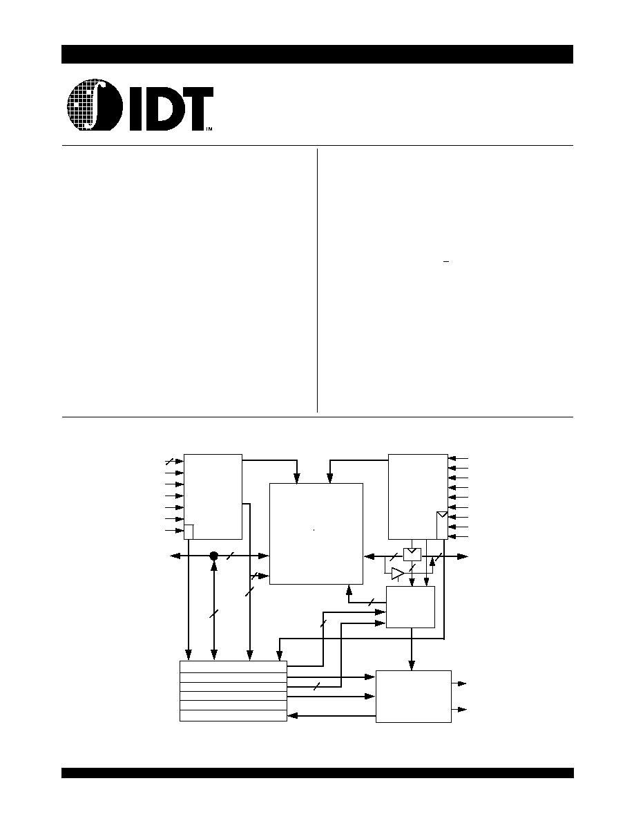
Random
Access
Port
Controls
Sequential
Access
Port
Controls
8K X 16
Memory
Array
Data
L
Data
R
Addr
L
Addr
R
I/O
0-15
SI/O
0-15
Pointer/
Counter
13
Start Address for Buffer #1
End Address for Buffer #1
Start Address for Buffer #2
End Address for Buffer #2
Flow Control Buffer
Flag Status
EOB
1
EOB
2
13
13
13
16
13
13
RST
COMPARATOR
LB
UB
A
0-12
13
CE
OE
R/
W
LSB
MSB
CMD
16
RST
SCLK
CNTEN
SOE
SSTRT
2
SCE
SR/
W
SLD
SSTRT
1
16
13
3016 drw 01
Reg.
,
HIGH SPEED 128K (8K X 16 BIT)
SEQUENTIAL ACCESS
RANDOM ACCESS MEMORY (SARAMTM)
Functional Block Diagram
IDT70825S/L
Features
x
x
x
x
x
High-speed access
≠ Military: 35/45ns (max.)
≠ Commercial: 20/25/35/45ns (max.)
x
x
x
x
x
Low-power operation
≠ IDT70825S
Active: 775mW (typ.)
Standby: 5mW (typ.)
≠ IDT70825L
Active: 775mW (typ.)
Standby: 1mW (typ.)
x
x
x
x
x
8K x 16 Sequential Access Random Access Memory
(SARAM
TM
)
≠ Sequential Access from one port and standard Random
Access from the other port
≠ Separate upper-byte and lower-byte control of the
Random Access Port
x
x
x
x
x
High speed operation
≠ 20ns t
AA
for random access port
≠ 20ns t
CD
for sequential port
≠ 25ns clock cycle time
x
x
x
x
x
Architecture based on Dual-Port RAM cells
x
x
x
x
x
Compatible with Intel BMIC and 82430 PCI Set
x
x
x
x
x
Width and Depth Expandable
x
x
x
x
x
Sequential side
≠ Address based flags for buffer control
≠ Pointer logic supports up to two internal buffers
x
x
x
x
x
Battery backup operation - 2V data retention
x
x
x
x
x
TTL-compatible, single 5V (+10%) power supply
x
x
x
x
x
Available in 80-pin TQFP and 84-pin PGA
x
x
x
x
x
Military product compliant to MIL-PRF-38535 QML
x
x
x
x
x
Industrial temperature range (-40∞C to +85∞C) is available
for selected speeds
Description
The IDT70825 is a high-speed 8K x 16-Bit Sequential Access
Random Access Memory (SARAM). The SARAM offers a single-chip
solution to buffer data sequentially on one port, and be accessed
randomly (asynchronously) through the other port. The device has a
2
IDT70825S/L
High-Speed 8K x 16 Sequential Access Random Access Memory Military, Industrial and Commercial Temperature Ranges
NOTES:
1. All V
CC
pins must be connected to power supply.
2. All GND pins must be connected to ground supply.
3. PN-80-1 package body is approximately 14mm x 14mm x 1.4mm.
G84-3 package body is approximately 1.21 in x 1.21 in x .16 in.
4. This package code is used to reference the package diagram.
5. This text does not indicate orientation of the actual part-marking.
Dual-Port RAM based architecture with a standard SRAM interface for
the random (asynchronous) access port, and a clocked interface with
counter sequencing for the sequential (synchronous) access port.
Fabricated using CMOS high-performance technology, this memory
device typically operates on less than 775mW of power at maximum
high-speed clock-to-data and Random Access. An automatic power
down feature, controlled by
CE, permits the on-chip circuitry of each
port to enter a very low standby power mode.
The IDT70825 is packaged in a 80-pin Thin Quad Flatpack (TQFP)
or 84-pin Pin Grid Array (PGA). Military grade product is manufactured
in compliance with the latest revision of MIL-PRF-38535 QML, making
it ideally suited to military temperature applications demanding the
highest level of performance and reliability.
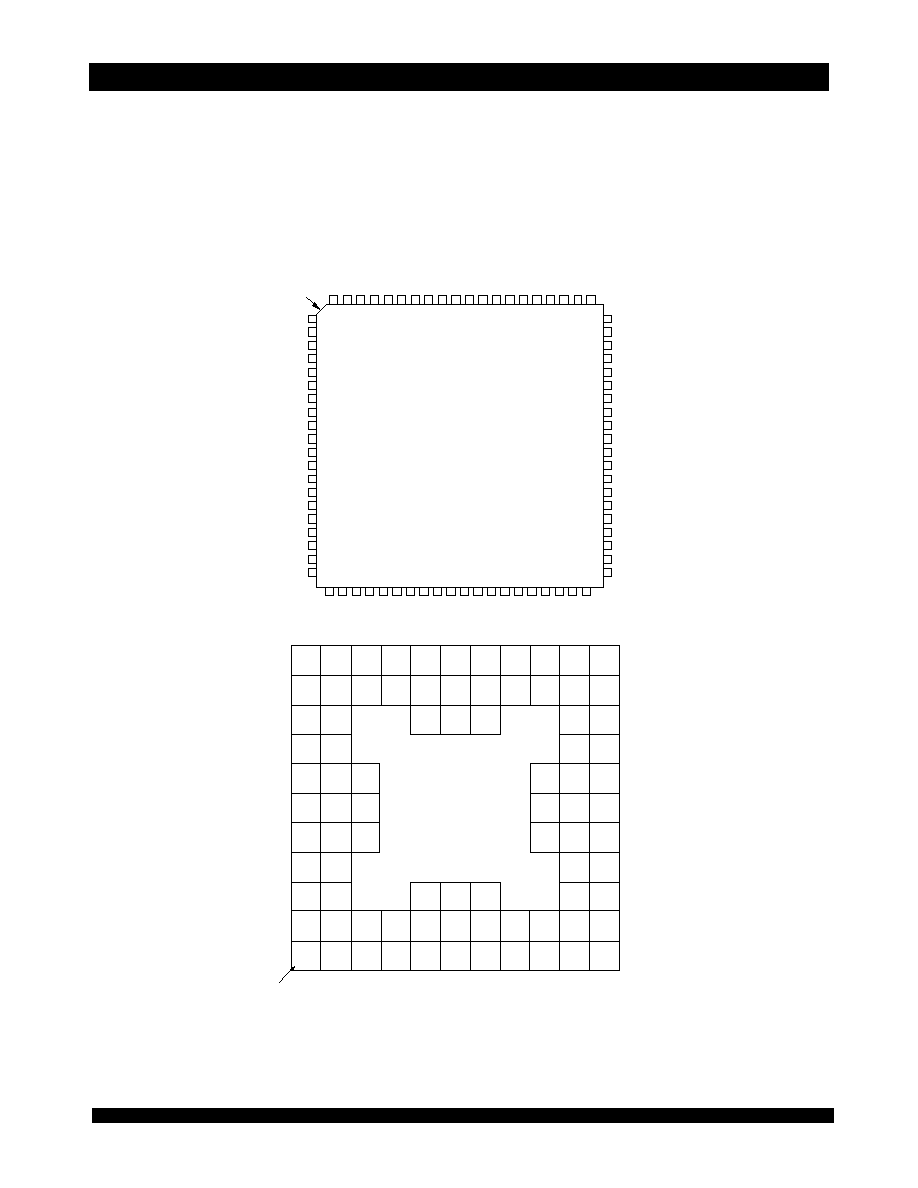
3016 drw 02
4
5
6
7
8
9
10
INDEX
11
12
13
14
1
80 79 78 77 76 75 74 73 72 71
23 24 25 26 27 28 29 30 31 32 33 34 35
3
2
15
16
17
18
19
20
21 22
36 37 38 39 40
41
42
43
62 61
60
59
58
57
56
55
54
53
52
63
64
51
50
49
48
47
46
45
44
70 69 68 67 66 65
IDT70825PF
PN80-1
(4)
80-PinTQFP
Top View
(5)
G
N
D
G
N
D
V
C
C
G
N
D
V
C
C
V
C
C
G
N
D
V
C
C
N
/
C
A
1
2
G
N
D
V
CC
A
10
A
9
A
8
A
7
A
6
A
5
A
4
A
3
A
1
A
2
CMD
CE
LB
UB
R/
W
OE
A
11
V
CC
A
0
SSTRT
1
SCLK
S
I
/
O
9
S
I
/
O
7
S
I
/
O
1
0
S
I
/
O
1
5
S
I
/
O
1
4
S
I
/
O
8
S
I
/
O
1
1
S
I
/
O
1
2
S
I
/
O
4
S
I
/
O
2
S
I
/
O
1
3
S
I
/
O
6
GND
SI/O
0
N/C
I/O
0
CNTEN
SLD
SCE
SR/
W
RST
SSTRT
2
SI/O
1
GND
GND
GND
EOB
2
V
CC
SOE
EOB
1
I
/
O
1
I
/
O
1
5
I
/
O
1
4
I
/
O
1
3
I
/
O
1
2
I
/
O
2
I
/
O
3
I
/
O
4
I
/
O
5
I
/
O
7
I
/
O
6
I
/
O
9
I
/
O
1
0
I
/
O
1
1
I
/
O
8
S
I
/
O
5
S
I
/
O
3
,
3016 drw 03
63
61
60
58
55
54
51
48
46
45
66
67
69
72
75
76
79
81
82
83
1
2
5
7
8
11
10
12
14
17
20
23
26
28
29
32
31
33
35
38
41
43
IDT70825G
G84-3
(4)
84-Pin PGA
Top View
(5)
A
B
C
D
E
F
G
H
J
K
L
42
59
56
49
50
40
25
27
30
36
34
37
39
84
3
4
6
9
15
13
16
18
22
24
19
21
68
71
70
77
80
11
10
09
08
07
06
05
04
03
02
01
64
65
62
57
53
52
47
44
73
74
78
A
3
NC
R/
W
UB
A
1
CE
A
5
A
6
A
8
A
9
A
11
I/O
14
NC
V
CC
CMD
A
2
NC SI/O
15
I/O
12
I/O
13
SI/O
14
SI/O
13
I/O
9
I/O
5
I/O
8
SI/O
9
SI/O
10
SI/O
6
I/O
4
SI/O
4
SI/O
5
I/O
3
GND
SSTRT
1
SCLK GND
SI/O
2
V
CC
I/O
7
I/O
6
GND
SI/O
8
SI/O
7
GND
NC
I/O
0
EOB
2
SOE RST SLD
SI/O
1
SI/O
3
SCE
SI/O
0
I/O
1
GND
CNTEN
GND
SSTRT
2
SR/
W
GND
NC
NC
V
CC
I/O
15
GND
OE
A
0
LB
V
CC
A
10
A
12
GND
A
4
A
7
I/O
10
V
CC
V
CC
SI/O
11
I/O
11
SI/O
12
I/O
2
V
CC
INDEX
EOB
1
Pin Configurations
(1,2,3)
6.42
IDT70825S/L
High-Speed 8K x 16 Sequential Access Random Access Memory Military, Industrial and Commercial Temperature Ranges
3
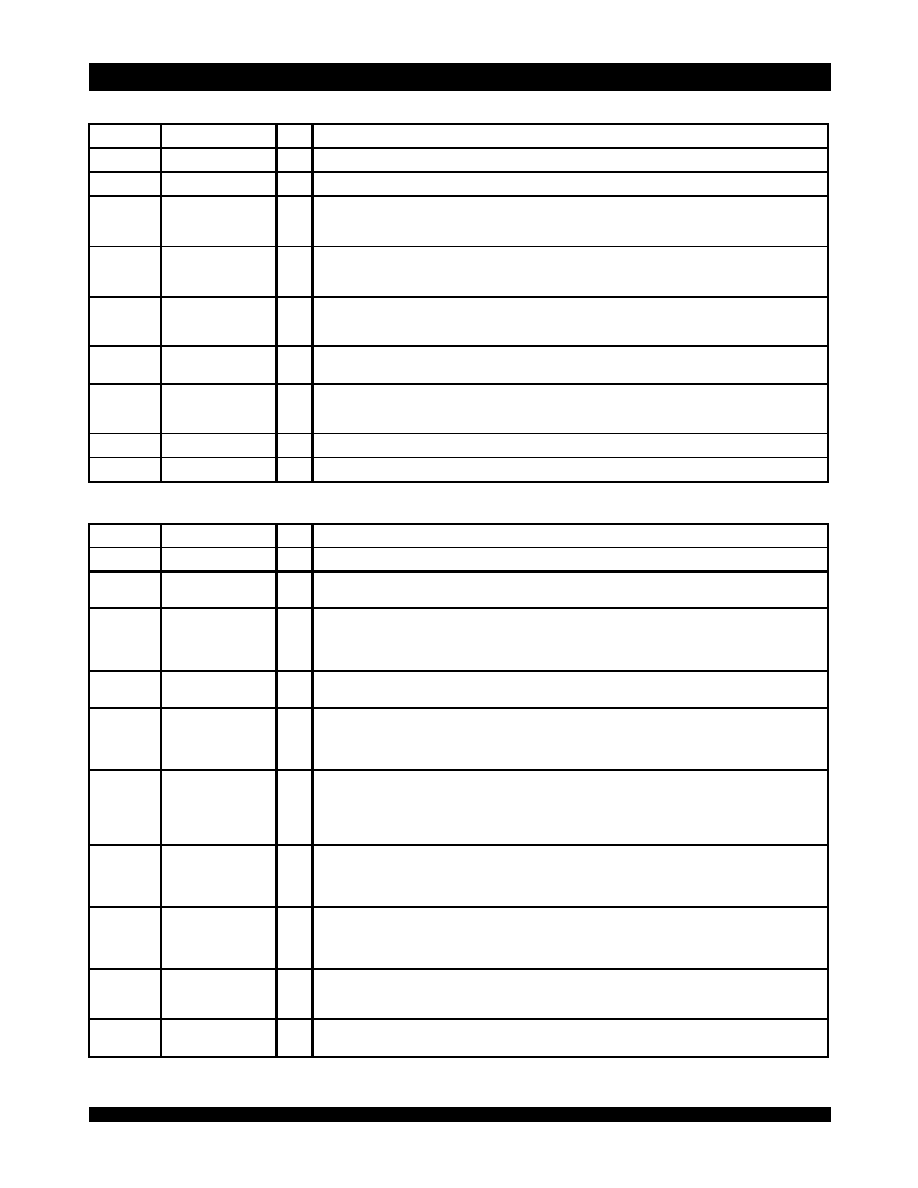
Pin Descriptions: Random Access Port
(1)
Pin Descriptions: Sequential Access Port
(1)
NOTE:
1. "I/O" is bidirectional input and output. "I" is input and "O" is output.
SYMBOL
NAME
I/O
DESCRIPTIONS
A
0-
A
12
Address Lines
I
Address inputs to access the 8192-word (16-Bit) memory array.
I/O
0
-I/O
15
Inputs/Outputs
I
Random access data inputs/outputs for 16-Bit wide data.
CE
Chip Enable
I
When
CE is LOW, the random access port is enabled. When CE is HIGH, the random access port is disabled
into power-down mode and the I/O outputs are in the High-impedance state. All data is retained during
CE =
V
IH
, unless it is altered by the sequential port.
CE and CMD may not be LOW at the same time.
CMD
Control Register
Enable
I
When
CMD is LOW, address lines A
0
-A
2
, R/W, and inputs/outputs I/O
0
-I/O
12
, are used to access the control
register, the flag register, and the start and end of buffer registers.
CMD and CE may not be LOW at the same
time.
R/
W
Read/Write Enable
I
If
CE is LOW and CMD is HIGH, data is written into the array when R/W is LOW and read o ut of the array when
R/
W is HIGH. If CE is HIGH and CMD is LOW, R/W is used to access the buffer command registers. CE and
CMD may not be LOW at the same time.
OE
Output Enable
I
When
OE is LOW and R/W is HIGH, I/O
0
-I/O
15
outputs are enabled. When
OE is HIGH, the I/O outputs are in
the High-impedance state.
LB, UB
Lower Byte, Upper
Byte Enables
I
When
LB is LOW, I/O
0
-I/O
7
are accessible for read and write operations. When
LB is HIGH I/O
0
-I/O
7
are tri-
stated and blocked during read and write operations.
UB controls access for I/O
8
-I/O
15
in the same manner and
is asynchronous from
LB.
V
CC
Power Supply
I
Seven +5V powe r supply pins. All V
CC
pins must be connected to the same +5V V
CC
supply.
GND
Ground
I
Ten ground pins. All ground pins must be connected to the same ground supply.
3016 tbl 01
SYMBOL
NAME
I/O
DESCRIPTIONS
SI/O
0-15
Inputs/Outputs
I
Sequential data inputs/outputs for 16-bit wide data.
SCLK
Clock
I
SI/O
0
-SI/O
15
,
SCE, SR/W, and SLD are registered on the LOW-to-HIGH transition of SCLK. Also, the sequential
access port address pointer increments by 1 on each LOW-to-HIGH transition of SCLK when
CNTEN is LOW.
SCE
Chip Enable
I
When
SCE is LOW, the sequential access port is enabled on the LOW-to-HIGH transition of SCLK. When SCE
is HIGH, the sequential access port is disabled into powere d-down mode on the LOW-to-HIGH transition of
SCLK, and the SI/O outputs are in the High-impedance state. All data is retained, unless altered by the random
access port.
CNTEN
Control Enable
I
When
CNTEN is LOW, the address pointer increments on the LOW-to-HIGH transition of SCLK. This function is
independent of
CE.
SR/
W
Read/Write Enable
I
When SR/
W and SCE are LOW, a write cycle is initiated on the LOW-to-HIGH transition of SCLK. When SR/W is
HIGH, and
SCE and SOE are LOW, a read cycle is initiated on the LOW-to-HIGH transition of SCLK. Termination
of a write cycle is done on the LOW-to-HIGH trans ition of SCLK if SR/
W or SCE is HIGH.
SLD
Address Pointer
Load Control
I
When
SLD is sampled LOW, there is an internal delay of one cycle before the address pointer changes. When
SLD is LOW, data on the inputs SI/O
0
-SI/O
12
is loaded into a data-in registe r on the LOW-to-HIGH transition of
SCLK. On the cycle following
SLD, the address pointer changes to the address location contained in the data-
in register.
SSTRT
1
and
SSTRT
2
may not be LOW while
SLD is LOW or during the cycle following SLD.
SSTRT
1
,
SSTRT
2
Load Start of
Address Register
I
When
SSTRT
1
or
SSTRT
2
is LOW, the start of address register #1 or #2 is loaded into the address pointer on
the LOW-to-HIGH transition of SCLK. The start address are stored in internal registers.
SSTRT
1
and
SSTRT
2
may not be LOW while
SLD is LOW or during the cycle following SLD.
EOB
1
,
EOB
2
End of Buffer Flag
I
EOB
1
or
EOB
2
is output LOW when the address pointer is incremented to match the addre ss stored in the end
of the buffer registers. The flags can be cleared by either asserting
RST LOW or by writing zero into Bit 0
and/or Bit 1 of the control register at address 101.
EOB
1
and
EOB
2
are dependent on separate internal
registers, and therefore separate match addresses.
SOE
Output Enable
I
SOE controls the data outputs and is independ ent of SCLK. When SOE is LOW, output buffers and the
sequentially addressed d ata is output. When
SOE is HIGH, the SI/O output bus is in the High-impedance state.
SOE is asynchronous to SCLK.
RST
Reset
I
When
RST is LOW, all internal registers are set to their default state, the address pointer is set to zero and the
EOB
1
and
EOB
2
flags are set HIGH. Rst is asynchronous to SCLK.
3016 tbl 02

4
IDT70825S/L
High-Speed 8K x 16 Sequential Access Random Access Memory Military, Industrial and Commercial Temperature Ranges
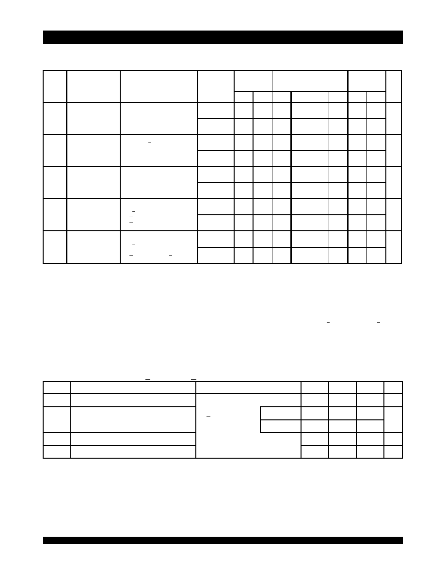
Absolute Maximum Ratings
(1)
Capacitance
(T
A
= +25∞C, f = 1.0mhz, TQFP only)
Recommended DC Operating
Conditions
Recommended Operating
Temperature and Supply Voltage
(1,2)
DC Electrical Characteristics Over the Operating
Temperature and Supply Voltage Range
(VCC = 5.0V ± 10%)
NOTES:
1. Stresses greater than those listed under ABSOLUTE MAXIMUM RATINGS may
cause permanent damage to the device. This is a stress rating only and functional
operation of the device at these or any other conditions above those indicated in the
operational sections of this specification is not implied. Exposure to absolute
maximum rating conditions for extended periods may affect reliability.
2. V
TERM
must not exceed Vcc + 10% for more than 25% of the cycle time or 10ns
maximum, and is limited to < 20mA for the period of V
TERM
>
Vcc + 10%.
NOTES:
1. This is the parameter T
A
.
2. Industrial temperature: for specific speeds, packages and powers contact your
sales office.
NOTES:
1. V
IL
> ≠1.5V for pulse width less than 10ns.
2.
V
TERM
must not exceed Vcc + 10%.
NOTES:
1. This parameter is determined by device characterization, but is not production
tested.
2. 3dV references the interpolated capacitance when the input and output signals
switch from 0V to 3V or from 3V to 0V.
Symbol
Rating
Commercial
& Industrial
Military
Unit
V
TERM
(2)
Terminal Voltage
with Respect
to GND
-0.5 to +7.0
-0.5 to +7.0
V
T
BIAS
Temperature
Under Bias
-55 to +125
-65 to +135
o
C
T
STG
Storage
Temperature
-55 to +125
-65 to +150
o
C
I
OUT
DC Output
Current
50
50
mA
3016 tbl 03
Grade
Ambient
Temperature
GND
Vcc
Military
-55
O
C to +125
O
C
0V
5.0V
+
10%
Commercial
0
O
C to +70
O
C
0V
5.0V
+
10%
Industrial
-40
O
C to +85
O
C
0V
5.0V
+
10%
3016 tbl 04
Symbol
Parameter
Min.
Typ.
Max.
Unit
V
CC
Supply Voltage
4.5
5.0
5.5
V
GND
Ground
0
0
0
V
V
IH
Input High Voltage
2.2
____
6.0
(2)
V
V
IL
Input Low Voltage
-0.5
(1)
____
0.8
V
3016 tbl 05
Symbol
Parameter
Conditions
(2)
Max.
Unit
C
IN
Input Capacitance
V
IN
= 3dV
9
pF
C
OUT
Output Capacitance
V
OUT
= 3dV
10
pF
3016 tbl 06
Symbol
Parameter
Test Conditions
70825S
70825L
Unit
Min.
Max.
Min.
Max.
|I
LI
|
Input Leakage Current
V
CC
= 5.5V, V
IN
= 0V to V
CC
___
5
___
1
µ A
|I
LO
|
Output Leakage Current
V
OUT
= 0V to V
CC
___
5
___
1
µ A
V
OL
Output Low Voltage
I
OL
= +4mA
___
0.4
___
0.4
V
V
OH
Output High Voltage
I
OH
= -4mA
2.4
___
2.4
___
V
3016 tbl 07
6.42
IDT70825S/L
High-Speed 8K x 16 Sequential Access Random Access Memory Military, Industrial and Commercial Temperature Ranges
5
DC Electrical Characteristics Over the Operating
Temperature and Supply Voltage Range
(1,2,8)
(V
CC
= 5.0V ± 10%)
Data Retention Characteristics Over All Temperature Ranges
(L Version Only)
(V
LC
< 0.2V, V
HC
> V
CC
- 0.2V)
NOTES:
1. 'X' in part number indicates power rating (S or L).
2. V
CC
= 5V, T
A
= +25∞C; guaranteed by device characterization but not production tested.
3. At f = f
MAX
, address, control lines (except Output Enable), and SCLK are cycling at the maximum frequency read cycle of 1/t
RC.
4. f = 0 means no address or control lines change.
5.
SCE may transition, but is LOW (SCE=V
IL
) when clocked in by SCLK.
6.
SCE may be - 0.2V, after it is clocked in, since SCLK=V
IH
must be clocked in prior to powerdown.
7. If one port is enabled (either
CE or SCE = LOW) then the other port is disabled (SCE or CE = HIGH, respectively). CMOS HIGH > Vcc - 0.2V and LOW < 0.2V, and
TTL HIGH = V
IH
and LOW = V
IL
.
8. Industrial temperature: for other speeds, packages and powers contact your sales office.
NOTES :
1. T
A
= +25∞C, V
CC
= 2V; guaranteed by device characterization but not production tested.
2. t
RC
= Read Cycle Time
3. This parameter is guaranteed by device characterization, but is not production tested.
4. To initiate data retention,
SCE = V
IH
must be clocked in.
70825X20
Com'l Only
70825X25
Com'l Only
70825X35
Com'l &
Military
70825X45
Com'l &
Military
Symbol
Parameter
Test Condition
Version
Typ.
Max.
Typ.
Max.
Typ.
Max.
Typ.
Max.
Unit
I
CC
Dynamic Operating
Current
(Both Ports Active)
CE = V
IL
,
Outputs Open
SCE = V
IL
(5)
f = f
MAX
(3)
COM'L
S
L
180
180
380
330
170
170
360
310
160
160
340
290
155
155
340
290
mA
MIL &
IND
S
L
____
____
____
____
____
____
____
____
160
160
400
340
155
155
400
340
I
SB1
Standby Current
(Both Ports - TTL
Level Inputs)
SCE and CE > V
IH
(7)
CMD = V
IH
f = f
MAX
(3)
COM'L
S
L
25
25
70
50
25
25
70
50
20
20
70
50
16
16
70
50
mA
MIL &
IND
S
L
____
____
____
____
____
____
____
____
20
20
85
65
16
16
85
65
I
SB2
Standby Current
(One Port - TTL
Level Inputs)
CE or SCE
= V
IH
Active Port Outputs Open,
f=f
MAX
(3)
COM'L
S
L
115
115
260
230
105
105
250
220
95
95
240
210
90
90
240
210
mA
MIL &
IND
S
L
____
____
____
____
____
____
____
____
95
95
290
250
90
90
290
250
I
SB3
Full Standby Current
(Both Ports -
CMOS Level Inputs)
Both Ports
CE and
SCE > V
CC
- 0.2V
(6,7)
V
IN
> V
CC
- 0.2V or
V
IN
< 0.2V, f = 0
(4)
COM'L
S
L
1.0
0.2
15
5
1.0
0.2
15
5
1.0
0.2
15
5
1.0
0.2
15
5
mA
MIL &
IND
S
L
____
____
____
____
____
____
____
____
1.0
0.2
30
10
1.0
0.2
30
10
I
SB4
Full Standby Current
(One Port -
CMOS Level Inputs)
One Port
CE or
SCE > V
CC
- 0.2V
(6)
Outputs Open (Active Port)
V
IN
> V
CC
- 0.2V or V
IN
< 0.2V
f = f
MAX
(3)
COM'L
S
L
110
110
240
200
100
100
230
190
90
90
220
180
85
85
220
180
mA
MIL &
IND
S
L
____
___
____
____
____
____
____
____
90
90
260
215
85
85
260
215
3016 tbl 08
Symbol
Parameter
Test Condition
Min.
Typ.
(1)
Max.
Unit
V
DR
V
CC
for Data Retention
V
CC
= 2V
2.0
___
___
V
I
CCDR
Data Retention Current
CE > V
HC
V
IN
= V
HC
or = V
LC
MIL. & IND.
___
100
4000
µ A
COM'L.
___
100
1500
t
CDR
(3)
Chip Deselect to Data Retention Time
SCE = V
HC
(4)
when SCLK =
CMD = V
HC
___
___
___
V
t
R
(3)
Operation Recovery Time
t
RC
(2)
___
___
V
3016 tbl 09