 | –≠–ª–µ–∫—Ç—Ä–æ–Ω–Ω—ã–π –∫–æ–º–ø–æ–Ω–µ–Ω—Ç: 70914 | –°–∫–∞—á–∞—Ç—å:  PDF PDF  ZIP ZIP |
©2000 Integrated Device Technology, Inc.
JANUARY 2001
DSC-3490/6
1
Features
x
x
x
x
x
High-speed clock-to-data output times
≠ Military: 20/25ns (max.)
≠ Commercial: 12/15/20ns (max.)
x
x
x
x
x
Low-power operation
≠ IDT70914S
Active: 850 mW (typ.)
Standby: 50 mW (typ.)
x
x
x
x
x
Architecture based on Dual-Port RAM cells
≠ Allows full simultaneous access from both ports
x
x
x
x
x
Synchronous operation
≠ 4ns setup to clock, 1ns hold on all control, data, and address
inputs
≠ Data input, address, and control registers
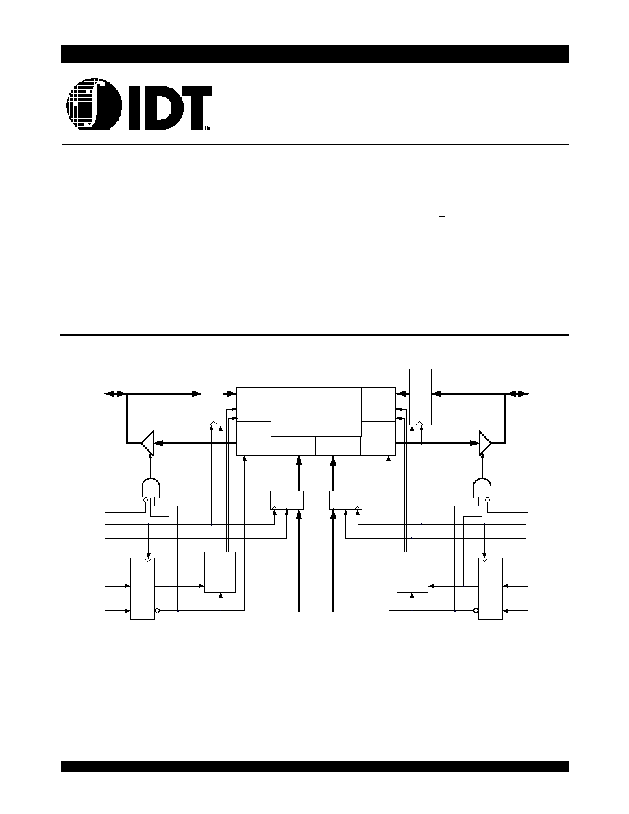
Functional Block Diagram
≠ Fast 12ns clock to data out
≠ Self-timed write allows fast cycle times
≠ 16ns cycle times, 60MHz operation
x
x
x
x
x
TTL-compatible, single 5V (+ 10%) power supply
x
x
x
x
x
Clock Enable feature
x
x
x
x
x
Guaranteed data output hold times
x
x
x
x
x
Available in 68-pin PLCC, and 80-pin TQFP
x
x
x
x
x
Military product compliant to MIL-PRF-38535 QML
x
x
x
x
x
Industrial temperature range (-40∞C to +85∞C) is available
for selected speeds.
x
x
x
x
x
Recommended for replacement of IDT7099 (4K x 9) if
separate 9th bit data control signals are not required.
HIGH SPEED 36K (4K X 9)
SYNCHRONOUS
DUAL-PORT RAM
IDT70914S
MEMOR
Y
ARRAY
I/O
0-8L
OE
L
CLK
L
CLKEN
L
R/
W
L
CE
L
Self-
timed
Write
Logic
REG
REG
en
REG
en
REGI
S
T
ER
REG
I
S
T
ER
MEMORY
ARRAY
WRITE
LOGIC
SENSE
AMPS
WRITE
LOGIC
SENSE
AMPS
DECODER DECODER
Self-
timed
Write
Logic
REG
I/O
0-8R
OE
R
CLK
R
CLKEN
R
R/
W
R
CE
R
3490 drw 01
A
0L
-A
11L
A
0R
-A
11R
6.42
IDT70914S
High-Speed 36K (4K x 9) Synchronous Dual-Port Static RAM Military, Industrial and Commercial Temperature Ranges
2
,
3490 drw 03
10
11
12
13
14
15
16
50
49
48
47
46
45
44
INDEX
17
18
19
20
21
22
23
24
25
26
51
52
53
54
55
56
57
58
59
60
9
8
7
6
5
4
3
2
1
68 67 66 65 64 63 62 61
27 28 29 30 31 32 33 34 35 36 37 38 39 40 41 42 43
A
6L
A
7L
A
8L
A
9L
A
10L
A
11L
OE
L
V
CC
R/
W
L
N/C
N/C
CE
L
GND
I/O
8L
I/O
7L
I/O
6L
N
/
C
I
/
O
5
L
V
C
C
I
/
O
4
L
I
/
O
3
L
I
/
O
2
L
I
/
O
1
L
I
/
O
0
L
G
N
D
G
N
D
I
/
O
0
R
I
/
O
1
R
I
/
O
2
R
I
/
O
3
R
V
C
C
I
/
O
4
R
I
/
O
5
R
A
7R
A
8R
A
9R
A
10R
A
11R
OE
R
GND
GND
R/
W
R
N/C
N/C
CE
R
GND
I/O
8R
I/O
7R
I/O
6R
A
5
L
A
4
L
A
3
L
A
2
L
A
1
L
A
0
L
C
L
K
E
N
L
C
L
K
L
C
L
K
R
C
L
K
E
N
R
A
0
R
A
1
R
A
2
R
A
3
R
A
4
R
A
5
R
A
6
R
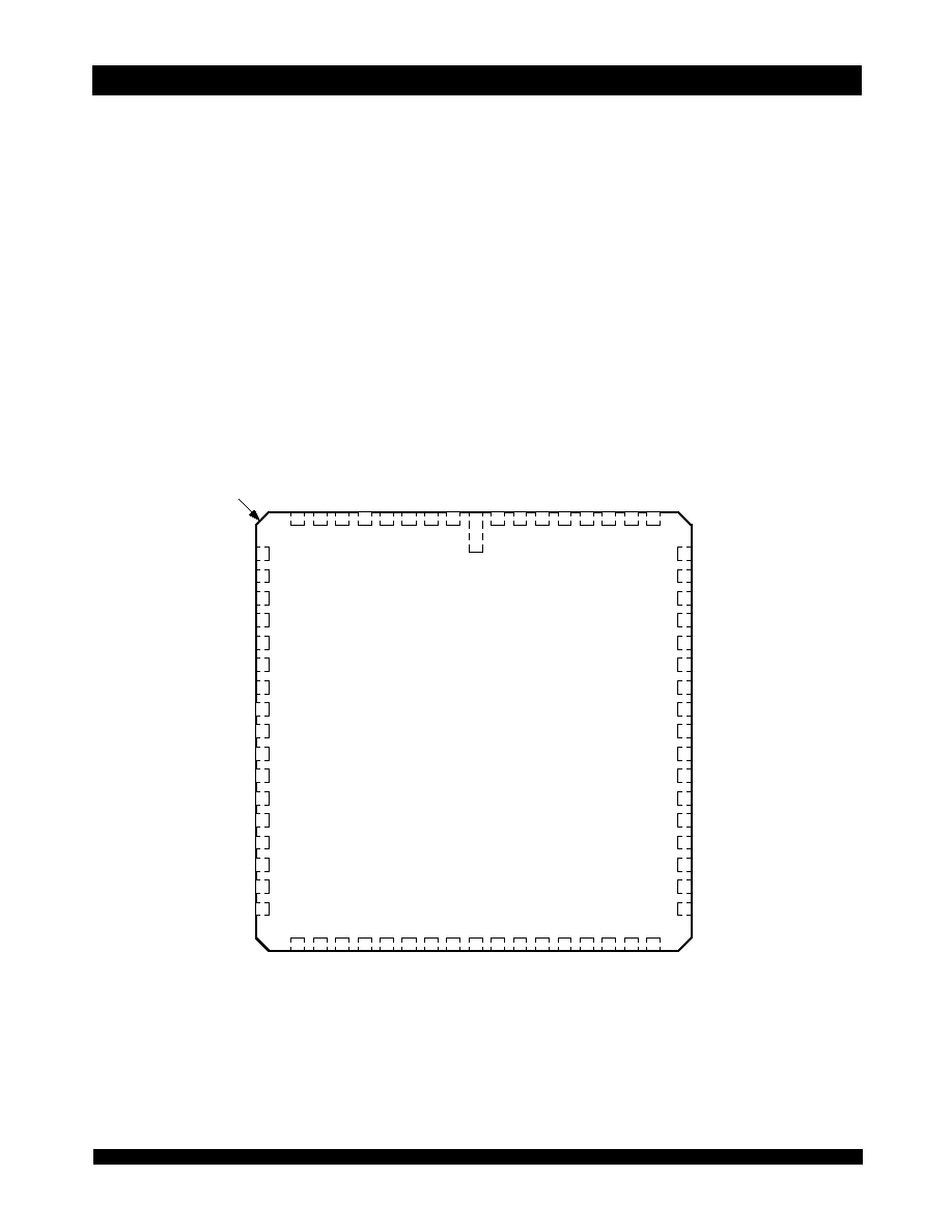
IDT70914J
J68-1
(4)
68-Pin PLCC
Top View
(5)
N/C
N/C
Pin Configurations
(1,2,3)
Description
The IDT70914 is a high-speed 4K x 9 bit synchronous Dual-Port RAM.
The memory array is based on Dual-Port memory cells to allow
simultaneous access from both ports. Registers on control, data, and
address inputs provide low set-up and hold times. The timing latitude
provided by this approach allow systems to be designed with very short
cycle times. With an input data register, this device has been optimized for
applications having unidirectional data flow or bi-directional data flow in
bursts.
The IDT70914 utilizes a 9-bit wide data path to allow for parity at the
user's option. This feature is especially useful in data communication
applications where it is necessary to use a parity bit for transmission/
reception error checking.
Fabricated using IDT's CMOS high-performance technology, these
Dual-Ports typically operate on only 850mW of power at maximum high-
speed clock-to-data output times as fast as 12ns. An automatic power
down feature, controlled by
CE, permits the on-chip circuitry of each port
to enter a very low standby power mode.
The IDT70914 is packaged in a 68-pin PLCC, and an 80-pin TQFP.
Military grade product is manufactured in compliance with the latest revision
of MIL-PRF-38535 QML, making it ideally suited for military temperature
applications demanding the highest level of performance and reliability.
NOTES:
1. All V
CC
pins must be connected to power supply.
2. All ground pins must be connected to ground supply.
3. J68-1 package body is approximately .95 in x .95 in x .17 in.
4. This package code is used to reference the package diagram.
5. This text does not indicate orientation of the actual part-marking.
6.42
IDT70914S
High-Speed 36K (4K x 9) Synchronous Dual-Port Static RAM Military, Industrial and Commercial Temperature Ranges
3
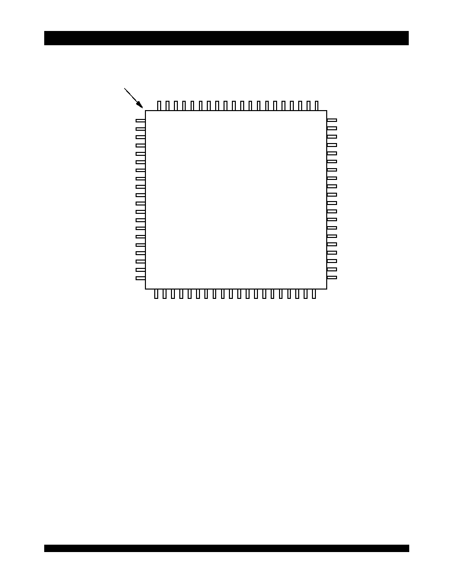
NOTES:
1. All V
CC
pins must be connected to power supply.
2. All ground pins must be connected to ground supply.
3. PN80-1 package body is approximately 14mm x 14mm x 1.4mm.
4. This package code is used to reference the package diagram.
5. This text does not indicate orientation of the actual part-marking.
Pin Configuration
(1,2,3)
(con't.)
Reference
N/C
1
2
3
4
5
6
7
8
9
10
11
12
13
14
15
16
17
18
19
20
21 22 23 24 25 26 27 28 29 30 31 32 33 34 35 36 37 38 39 40
80 79 78 77 76 75 74 73 72 71 70 69 68 67 66 65 64 63 62 61
60
59
58
57
56
55
54
53
52
51
50
49
48
47
46
45
44
43
42
41
3490 drw 04
IDT70914PF
PN80-1
(4)
80-Pin TQFP
Top View
(5)
N/C
A
6L
A
7L
A
8L
A
9L
A
10L
A
11L
N/C
OE
L
V
CC
R/
W
L
N/C
CE
L
GND
I/O
8L
I/O
7L
I/O
6L
N/C
A
7R
A
8R
A
9R
A
10R
A
1
1R
N/C
OE
R
GND
GND
R/
W
R
N/C
CE
R
GND
I/O
8R
I/O
7R
I/O
6R
N/C
C
L
K
E
N
L
C
L
K
E
N
R
N/C
N/C
N/C
N/C
N
/
C
N
/
C
I
/
O
5
L
V
C
C
I
/
O
4
L
I
/
O
3
L
I
/
O
2
L
I
/
O
1
L
I
/
O
0
L
G
N
D
G
N
D
I
/
O
0
R
I
/
O
1
R
I
/
O
2
R
I
/
O
3
R
V
C
C
I
/
O
4
R
I
/
O
5
R
N
/
C
N
/
C
N
/
C
N
/
C
A
5
L
A
4
L
A
3
L
A
2
L
A
1
L
A
0
L
C
L
K
L
C
L
K
R
A
0
R
A
1
R
A
2
R
A
3
R
A
4
R
A
5
R
A
6
R
N
/
C
,
6.42
IDT70914S
High-Speed 36K (4K x 9) Synchronous Dual-Port Static RAM Military, Industrial and Commercial Temperature Ranges
4
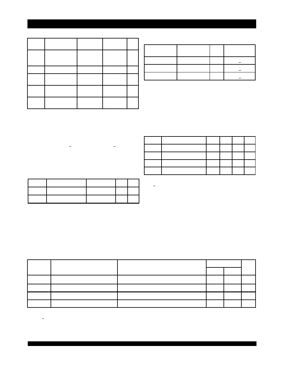
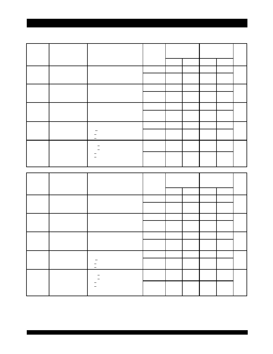
DC Electrical Characteristics Over the Operating
Temperature and Supply Voltage Range
(V
CC
= 5.0V ± 10%)
Recommended DC Operating
Conditions
NOTES:
1. Stresses greater than those listed under ABSOLUTE MAXIMUM RATINGS may
cause permanent damage to the device. This is a stress rating only and functional
operation of the device at these or any other conditions above those indicated
in the operational sections of this specification is not implied. Exposure to absolute
maximum rating conditions for extended periods may affect reliability.
2. V
TERM
must not exceed V
CC
+ 10% for more than 25% of the cycle time or 10ns
maximum, and is limited to < 20mA for the period of V
TERM
> V
cc
+ 10%.
Absolute Maximum Ratings
(1)
Maximum Operating Temperature
and Supply Voltage
(1,2)
NOTES:
1. These parameters are determined by device characterization, but are not
production tested.
2. 3dV references the interpolated capacitance when the input and output switch
from 0V to 3V or from 3V to 0V.
Capacitance
(T
A
= +25∞C, f = 1.0MH
z
)
TQFP Only
NOTES:
1. This is the parameter T
A
. This is the "instant on" casae temperature.
2. Industrial temperature: for specific speeds, packages and powers contact your
NOTES:
1. V
IL
> -1.5V for pulse width less than 10ns.
2. V
TERM
must not exceed V
CC
+ 10%.
NOTE:
1. At V
CC
< 2.0V, input leakages are undefined
Symbol
Rating
Commercial
& Industrial
Military
Unit
V
TERM
(2)
Terminal Voltage
with Respect
to GND
-0.5 to +7.0
-0.5 to +7.0
V
V
TERM
(2)
Terminal Voltage
-0.5 to V
CC
-0.5 to V
CC
V
T
BIAS
Temperature
Under Bias
-55 to +125
-65 to +135
o
C
T
STG
Storage
Temperature
-65 to +150
-65 to +150
o
C
I
OUT
DC Output
Current
50
50
mA
3490 tbl 01
Grade
Ambient
Temperature
GND
V
CC
Military
-55
O
C to+125
O
C
0V
5.0V
+
10%
Commercial
0
O
C to +70
O
C
0V
5.0V
+
10%
Industrial
-40
O
C to +85
O
C
0V
5.0V
+
10%
3490 tbl 02
Symbol
Parameter
Min.
Typ.
Max.
Unit
V
CC
Supply Voltage
4.5
5.0
5.5
V
GND
Ground
0
0
0
V
V
IH
Input High Voltage
2.2
____
6.0
(2)
V
V
IL
Input Low Voltage
-0.5
(1)
____
0.8
V
3490 tbl 03
Symbol
Parameter
Conditions
Max.
Unit
C
IN
Input Capacitance
V
IN
= 3dV
8
pF
C
OUT
Output Capacitance
V
OUT
= 3dV
9
pF
3490 tbl 04
Symbol
Parameter
Test Conditions
70914S
Unit
Min.
Max.
|I
LI
|
Input Leakage Current
(1)
V
CC
= 5.5V, V
IN
= 0V to V
CC
___
10
µ A
|I
LO
|
Output Leakage Current
CE = V
IH
, V
OUT
= 0V to V
CC
___
10
µ A
V
OL
Output Low Voltage
I
OL
= +4mA
___
0.4
V
V
OH
Output High Voltage
I
OH
= -4mA
2.4
___
V
3490 tbl 05
6.42
IDT70914S
High-Speed 36K (4K x 9) Synchronous Dual-Port Static RAM Military, Industrial and Commercial Temperature Ranges
5
DC Electrical Characteristics Over the Operating
Temperature and Supply Voltage Range
(4,5)
(V
CC
= 5V ± 10%)
NOTES:
1. At f
MAX
, address and control lines (except Output Enable) are cycling at the maximum frequency clock cycle of 1/t
CYC
, using "AC TEST CONDITIONS" at input levels
of GND to 3V.
2. f = 0 means no address, clock, or control lines change. Applies only to input at CMOS level standby.
3. Port "A" may be either left or right port. Port "B" is the opposite from port "A".
4. Vcc = 5V, T
A
= 25∞C for Typ, and are not production tested. I
CC DC
= 150mA (Typ).
5. Industrial temperature: for specific speeds, packages and powers contact your sales office.
70914S12
Com 'l Only
70914S15
Com 'l Only
S ym bol
P aram eter
Test Condition
V ersion
Typ.
(2)
M ax.
Typ.
(2)
M ax.
Unit
I
CC
Dynam ic O p e rating
Curre nt
(B o th P o rts A c tiv e )
CE
L
and
CE
R
= V
IL
,
O utp uts Dis ab le d
f = f
M A X
(1)
CO M 'L
190
310
180
300
m A
M IL &
IND
____
____
____
____
I
S B 1
S tand b y Curre nt
(B o th P o rts - TTL
Le ve l Inp uts )
CE
L
and
CE
R
= V
IH
f = f
M A X
(1)
CO M 'L
95
150
90
140
m A
M IL &
IND
____
____
____
____
I
S B 2
S tand b y Curre nt
(One P o rt - TTL
Le ve l Inp uts )
CE
"A "
= V
IL
and
CE
"B "
= V
IH
(3)
A c tiv e P o rt O utp uts
Disab le d , f= f
M A X
(1)
CO M 'L
170
220
160
210
m A
M IL &
IND
____
____
____
____
I
S B 3
Full S tand b y
Curre nt (B o th
P o rts - A ll CM O S
Le ve l Inp uts )
B o th P o rts
CE
R
and
CE
L
> V
CC
- 0.2V
V
IN
> V
CC
- 0.2V o r
V
IN
< 0.2V , f = 0
(2)
CO M 'L
10
15
10
15
m A
M IL &
IND
____
____
____
____
I
S B 4
Full S tand b y
Curre nt (O ne
P o rt - A ll CM O S
Le ve l Inp uts )
CE
"A "
< 0.2V and
CE
"B "
> V
CC
- 0.2V
(3)
V
IN
> V
CC
- 0.2V o r
V
IN
< 0.2V, A c tiv e P o rt
O utp uts Dis ab le d
f = f
M A X
(1)
CO M 'L
165
210
155
200
m A
M IL &
IND
____
____
____
____
3 490 tb l 06 a
70914S20
Com 'l &
M ilitary
70914S25
M ilitary
Only
S ym bol
P aram eter
Test Condition
V ersion
Typ.
(2)
M ax.
Typ.
(2)
M ax.
Unit
I
CC
Dynam ic O p e rating
Curre nt
(B o th P o rts A c tiv e )
CE
L
and
CE
R
= V
IL
,
O utp uts Dis ab le d
f = f
M A X
(1)
CO M 'L
170
290
____
____
m A
M IL &
IND
170
310
160
290
I
S B 1
S tand b y Curre nt
(B o th P o rts - TTL
Le ve l Inp uts )
CE
L
and
CE
R
= V
IH
f = f
M A X
(1)
CO M 'L
85
130
____
____
m A
M IL &
IND
85
140
80
130
I
S B 2
S tand b y Curre nt
(One P o rt - TTL
Le ve l Inp uts )
CE
"A "
= V
IL
and
CE
"B "
= V
IH
(3)
A c tiv e P o rt O utp uts
Disab le d , f= f
M A X
(1)
CO M 'L
150
200
____
____
m A
M IL &
IND
150
210
140
200
I
S B 3
Full S tand b y
Curre nt (B o th
P o rts - A ll CM O S
Le ve l Inp uts )
B o th P o rts
CE
R
and
CE
L
> V
CC
- 0.2V
V
IN
> V
CC
- 0.2V o r
V
IN
< 0.2V , f = 0
(2)
CO M 'L
10
15
____
____
m A
M IL &
IND
10
20
10
20
I
S B 4
Full S tand b y
Curre nt (O ne
P o rt - A ll CM O S
Le ve l Inp uts )
CE
"A "
< 0.2V and
CE
"B "
> V
CC
- 0.2V
(3)
V
IN
> V
CC
- 0.2V o r
V
IN
< 0.2V, A c tiv e P o rt
O utp uts Dis ab le d
f = f
M A X
(1)
CO M 'L
145
190
____
____
m A
M IL &
IND
145
200
135
190
3490 tb l 0 6b