 | –≠–ª–µ–∫—Ç—Ä–æ–Ω–Ω—ã–π –∫–æ–º–ø–æ–Ω–µ–Ω—Ç: 70T3319 | –°–∫–∞—á–∞—Ç—å:  PDF PDF  ZIP ZIP |
©2003 Integrated Device Technology, Inc.
APRIL 2003
DSC-5652/2
1
HIGH-SPEED 2.5V
512/256/128K X 18
SYNCHRONOUS
DUAL-PORT STATIC RAM
WITH 3.3V OR 2.5V INTERFACE
PRELIMINARY
IDT70T3339/19/99S
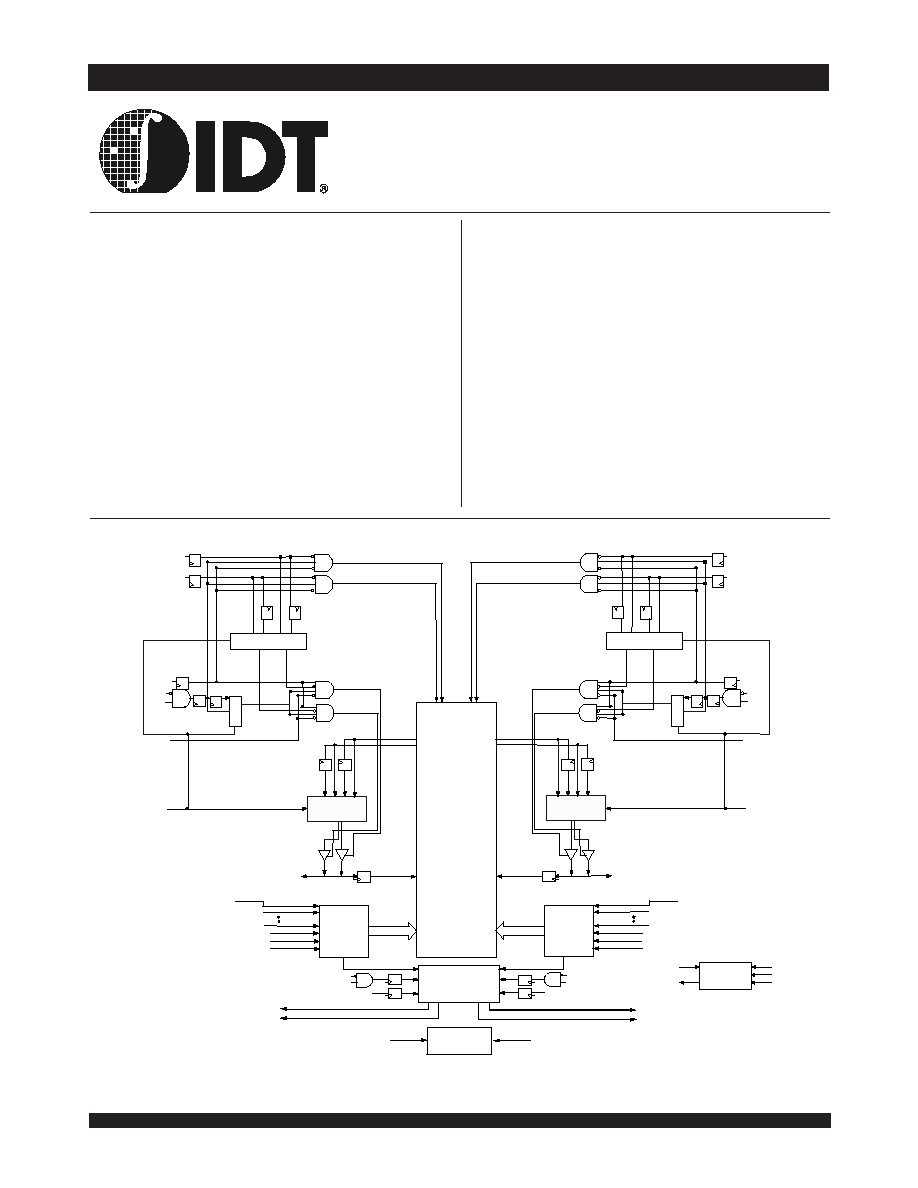
Functional Block Diagram
≠ Data input, address, byte enable and control registers
≠ Self-timed write allows fast cycle time
Separate byte controls for multiplexed bus and bus
matching compatibility
Dual Cycle Deselect (DCD) for Pipelined Output Mode
2.5V (±100mV) power supply for core
LVTTL compatible, selectable 3.3V (±150mV) or 2.5V
(±100mV) power supply for I/Os and control signals on
each port
Industrial temperature range (-40∞C to +85∞C) is
available at 166MHz and 133MHz
Available in a 256-pin Ball Grid Array (BGA), a 144-pin Thin
Quad Flatpack (TQFP) and 208-pin fine pitch Ball Grid Array
(fpBGA)
Supports JTAG features compliant with IEEE 1149.1
Due to limited pin count JTAG, Collision Detection and
Interrupt are not supported on the 144-pin TQFP package
Features:
True Dual-Port memory cells which allow simultaneous
access of the same memory location
High-speed data access
≠ Commercial: 3.4 (200MHz)/3.6ns (166MHz)/
4.2ns (133MHz)(max.)
≠ Industrial: 3.6ns (166MHz)/4.2ns (133MHz) (max.)
Selectable Pipelined or Flow-Through output mode
Counter enable and repeat features
Dual chip enables allow for depth expansion without
additional logic
Interrupt and Collision Detection Flags
Full synchronous operation on both ports
≠ 5ns cycle time, 200MHz operation (14Gbps bandwidth)
≠ Fast 3.4ns clock to data out
≠ 1.5ns setup to clock and 0.5ns hold on all control, data, and
address inputs @ 200MHz
1. Address A
18
is a NC for the IDT70T3319. Also, Addresses A
18
and A
17
are NC's for the IDT70T3399.
2. The sleep mode pin shuts off all dynamic inputs, except JTAG inputs, when asserted. All static inputs, i.e., PL/FTx and
OPTx and the sleep mode pins themselves (ZZx) are not affected during sleep mode.
NOTES:
Dout0-8_L
B
W
0
L
B
W
1
L
Din_L
OE
L
UB
L
LB
L
R/
W
L
CE
0L
CE
1L
a b
FT
/PIPE
L
0/1
1b 0b 1a 0a
1
0
1/0
0b 1b
0a 1a
a
b
FT
/PIPE
L
1/0
REPEAT
R
A
0R
CNTEN
R
ADS
R
Dout0-8_R
Dout9-17_R
I/O
0R
- I/O
17R
Din_R
ADDR_R
OE
R
UB
R
LB
R
R/
W
R
CE
0R
CE
1R
FT
/PIPE
R
CLK
R
,
Counter/
Address
Reg.
B
W
1
R
B
W
0
R
FT
/PIPE
R
Counter/
Address
Reg.
CNTEN
L
ADS
L
REPEAT
L
Dout9-17_L
I/O
0L
- I/O
17L
A
18L
(1)
A
0L
ADDR_L
5652 drw 01
512/256/128K x 18
MEMORY
ARRAY
CLK
L
,
b a
0/1
0b
1b
0a 1a
1
0
1/0
1b 0b
1a 0a
a
b
1/0
INTERRUPT
COLLISION
DETECTION
LOGIC
INT
L
COL
L
INT
R
COL
R
R/
W
L
R /
W
R
CE
0 L
CE1L
CE
0 R
CE1R
ZZ
CONTROL
LOGIC
ZZ
L
(2)
ZZ
R
(2)
JTAG
TCK
TRST
TMS
TDO
TDI
A
18R
(1)

6.42
IDT70T3339/19/99S
PRELIMINARY
High-Speed 2.5V 512/256/128K x 18 Dual-Port Static RAM Industrial and Commercial Temperature Ranges
2
Description:
The IDT70T3339/19/99 is a high-speed 512/256/128k x 18 bit
synchronous Dual-Port RAM. The memory array utilizes Dual-Port
memory cells to allow simultaneous access of any address from both ports.
Registers on control, data, and address inputs provide minimal setup and
hold times. The timing latitude provided by this approach allows systems
to be designed with very short cycle times. With an input data register, the
IDT70T3339/19/99 has been optimized for applications having unidirec-
tional or bidirectional data flow in bursts. An automatic power down feature,
controlled by CE
0
and CE
1,
permits the on-chip circuitry of each port to
enter a very low standby power mode.
The IDT70T3339/19/99 can support an operating voltage of either
3.3V or 2.5V on one or both ports, controllable by the OPT pins. The power
supply for the core of the device (V
DD
) is at 2.5V.

6.42
IDT70T3339/19/99S
PRELIMINARY
High-Speed 2.5V 512/256/128K x 18 Dual-Port Static RAM Industrial and Commercial Temperature Ranges
3
70T3339/19/99BC
BC-256
(8)
256-Pin BGA
Top View
(9)
Pin Configuration
(3,4,5,6,9)
NOTES:
1. Pin is a NC for IDT70T3319 and IDT70T3399.
2. Pin is a NC for IDT70T3399.
3. All V
DD
pins must be connected to 2.5V power supply.
4. All V
DDQ
pins must be connected to appropriate power supply: 3.3V if OPT pin for that port is set to V
DD
(2.5V), and 2.5V if OPT pin for that port is
set to V
SS
(0V).
5. All V
SS
pins must be connected to ground supply.
6. Package body is approximately 17mm x 17mm x 1.4mm, with 1.0mm ball-pitch.
7. This package code is used to reference the package diagram.
8. This text does not indicate orientation of the actual part-marking.
9. Pins A15 and T15 will be V
REFL
and V
REFR
respectively for future HSTL device.
E16
I/O
7R
D16
I/O
8R
C16
I/O
8L
B16
NC
A16
NC
A15
NC
B15
NC
C15
NC
D15
NC
E15
I/O
7L
E14
NC
D14
NC
D13
V
DD
C12
A
6L
C14
OPT
L
B14
V
DD
A14
A
0L
A12
A
5L
B12
A
4L
C11
ADS
L
D12
V
DDQR
D11
V
DDQR
C10
CLK
L
B11
REPEAT
L
A11
CNTEN
L
D8
V
DDQR
C8
NC
A9
CE
1L
D9
V
DDQL
C9
LB
L
B9
CE
0L
D10
V
DDQL
C7
A
7L
B8
UB
L
A8
NC
B13
A
1L
A13
A
2L
A10
OE
L
D7
V
DDQR
B7
A
9L
A7
A
8L
B6
A
12L
C6
A
10L
D6
V
DDQL
A5
A
14L
B5
A
15L
C5
A
13L
D5
V
DDQL
A4
A
17L
(2)
B4
A
18L
(1)
C4
A
16L
D4
PIPE/
FT
L
A3
NC
B3
TDO
C3
V
SS
D3
NC
D2
I/O
9R
C2
I/O
9L
B2
NC
A2
TDI
A1
NC
B1
INT
L
C1
COL
L
D1
NC
E1
I/O
10R
E2
I/O
10L
E3
NC
E4
V
DDQL
F1
I/O
11L
F2
NC
F4
V
DDQL
G1
NC
G2
NC
G3
I/O
12L
G4
V
DDQR
H1
NC
H2
I/O
12R
H3
NC
H4
V
DDQR
J1
I/O
13L
J2
I/O
14R
J3
I/O
13R
J4
V
DDQL
K1
NC
K2
NC
K3
I/O
14L
K4
V
DDQL
L1
I/O
15L
L2
NC
L3
I/O
15R
L4
V
DDQR
M1
I/O
16R
M2
I/O
16L
M3
NC
M4
V
DDQR
N1
NC
N2
I/O
17R
N3
NC
N4
PIPE/
FT
R
P1
COL
R
P2
I/O
17L
P3
TMS
P4
A
16R
R1
INT
R
R2
NC
R3
TRST
R4
A
18R
(1)
T1
NC
T2
TCK
T3
NC
T4
A
17R
(2)
P5
A
13R
R5
A
15R
P12
A
6R
P8
NC
P9
LB
R
R8
UB
R
T8
NC
P10
CLK
R
T11
CNTEN
R
P11
ADS
R
R12
A
4R
T12
A
5R
P13
A
3R
P7
A
7R
R13
A
1R
T13
A
2R
R6
A
12R
T5
A
14R
T14
A
0R
R14
OPT
R
P14
NC
P15
NC
R15
NC
T15
NC
T16
NC
R16
NC
P16
I/O
0L
N16
NC
N15
I/O
0R
N14
NC
M16
NC
M15
I/O
1L
M14
I/O
1R
L16
I/O
2R
L15
NC
L14
I/O
2L
K16
I/O
3L
K15
NC
K14
NC
J16
I/O
4L
J15
I/O
3R
J14
I/O
4R
H16
I/O
5R
H15
NC
H14
NC
G16
NC
G15
NC
G14
I/O
5L
F16
I/O
6L
F14
I/O
6R
F15
NC
R9
CE
0R
R11
REPEAT
R
T6
A
11R
T9
CE
1R
A6
A
11L
B10
R/
W
L
C13
A
3L
P6
A
10R
R10
R/
W
R
R7
A
9R
T10
OE
R
T7
A
8R
,
E5
V
DD
E6
V
DD
E7
NC
E8
V
SS
E9
V
SS
E10
V
SS
E11
V
DD
E12
V
DD
E13
V
DDQR
F5
V
DD
F6
NC
F8
V
SS
F9
V
SS
F10
V
SS
F12
V
DD
F13
V
DDQR
G5
V
SS
G6
V
SS
G7
V
SS
G8
V
SS
G9
V
SS
G10
V
SS
G11
V
SS
G12
V
SS
G13
V
DDQL
H5
V
SS
H7
V
SS
H8
V
SS
H9
V
SS
H10
V
SS
H11
V
SS
H12
V
SS
H13
V
DDQL
J5
ZZ
R
J6
V
SS
J7
V
SS
J8
V
SS
J9
V
SS
J10
V
SS
J11
V
SS
J12
ZZ
L
J13
V
DDQR
K5
V
SS
K6
V
SS
K7
V
SS
K8
V
SS
L5
V
DD
L6
NC
L7
NC
L8
V
SS
M5
V
DD
M6
V
DD
M7
NC
M8
V
SS
N5
V
DDQR
N6
V
DDQR
N7
V
DDQL
N8
V
DDQL
K9
V
SS
K10
V
SS
K11
V
SS
K12
V
SS
L9
V
SS
L10
V
SS
L11
V
SS
L12
V
DD
M9
V
SS
M10
V
SS
M11
V
DD
M12
V
DD
N9
V
DDQR
N10
V
DDQR
N11
V
DDQL
N12
V
DDQL
K13
V
DDQR
L13
V
DDQL
M13
V
DDQL
N13
V
DD
F7
NC
F11
V
SS
5652 drw 02d
,
F3
I/O
11R
01/13/03
H6
V
SS

6.42
IDT70T3339/19/99S
PRELIMINARY
High-Speed 2.5V 512/256/128K x 18 Dual-Port Static RAM Industrial and Commercial Temperature Ranges
4
Pin Configuration(con't)
(3,4,5,6,9,10)
NOTES:
3. All V
DD
pins must be connected to 2.5V power supply.
4. All V
DDQ
pins must be connected to appropriate power supply: 3.3V if OPT pin for that port is set to V
DD
(2.5V), and 2.5V if OPT pin for that port is set to V
SS
(0V).
5. All V
SS
pins must be connected to ground supply.
6. Package body is approximately 20mm x 20mm x 1.4mm.
7. This package code is used to reference the package diagram.
8. This text does not indicate orientation of the actual part-marking.
9. Due to limited pin count, JTAG, Collison Detection and Interrupt are not supported in the DD-144 package.
10. Pins 109 and 72 will be V
REFL
and V
REFR
respectively for future HSTL device.
1. Pin is a NC for IDT70T3319 and IDT70T3399.
2. Pin is a NC for IDT70T3399.
V
SS
V
DDQR
V
SS
I/O
9L
I/O
9R
I/O
10L
I/O
10R
I/O
11L
I/O
11R
V
DDQL
V
SS
I/O
12L
I/O
12R
V
DDQR
ZZ
R
V
DD
V
DD
V
SS
V
SS
V
DDQL
V
SS
I/O
13R
I/O
13L
I/O
14R
I/O
14L
V
DDQR
V
SS
I/O
15R
I/O
15L
I/O
16R
I/O
16L
I/O
17R
I/O
17L
V
SS
V
DDQL
NC
1
2
3
4
5
6
7
8
9
10
11
12
13
14
15
16
17
18
19
20
21
22
23
24
25
26
27
28
29
30
31
32
33
34
35
36
3
7
3
8
3
9
4
0
4
1
4
2
4
3
4
4
4
5
4
6
4
7
4
8
4
9
5
0
5
1
5
2
5
3
5
4
5
5
5
6
5
7
5
8
5
9
6
0
6
1
6
2
6
3
6
4
6
5
6
6
6
7
6
8
6
9
7
0
7
1
7
2
108
107
106
105
104
103
102
101
100
99
98
97
96
95
94
93
92
91
90
89
88
87
86
85
84
83
82
81
80
79
78
77
76
75
74
73
1
4
4
1
4
3
1
4
2
1
4
1
1
4
0
1
3
9
1
3
8
1
3
7
1
3
6
1
3
5
1
3
4
1
3
3
1
3
2
1
3
1
1
3
0
1
2
9
1
2
8
1
2
7
1
2
6
1
2
5
1
2
4
1
2
3
1
2
2
1
2
1
1
2
0
1
1
9
1
1
8
1
1
7
1
1
6
1
1
5
1
1
4
1
1
3
1
1
2
1
1
1
1
1
0
1
0
9
P
L
/
F
T
R
N
C
N
C
A
1
8
R
(
1
)
A
1
7
R
(
2
)
A
1
6
R
A
1
5
R
A
1
4
R
A
1
3
R
A
1
2
R
A
1
1
R
A
1
0
R
A
9
R
A
8
R
A
7
R
U
B
R
L
B
R
C
E
1
R
C
E
0
R
V
D
D
V
S
S
C
L
K
R
O
E
R
R
/
W
R
A
D
S
R
C
N
T
E
N
R
R
E
P
E
A
T
R
A
6
R
A
5
R
A
4
R
A
3
R
A
2
R
A
1
R
A
0
R
V
D
D
N
C
OPT
L
V
DDQR
V
SS
I/O
8L
I/O
8R
I/O
7L
I/O
7R
I/O
6L
I/O
6R
V
SS
V
DDQL
I/O
5L
I/O
5R
V
SS
V
DDQR
V
DD
V
DD
V
SS
V
SS
ZZ
L
V
DDQL
I/O
4R
I/O
4L
I/O
3R
I/O
3L
V
SS
V
DDQR
I/O
2R
I/O
2L
I/O
1R
I/O
1L
I/O
0R
I/O
0L
V
SS
V
DDQL
OPT
R
P
L
/
F
T
L
N
C
N
C
A
1
8
L
(
1
)
A
1
7
L
(
2
)
A
1
6
L
A
1
5
L
A
1
4
L
A
1
3
L
A
1
2
L
A
1
1
L
A
1
0
L
A
9
L
A
8
L
A
7
L
U
B
L
L
B
L
C
E
1
L
C
E
0
L
V
D
D
V
S
S
C
L
K
L
O
E
L
R
/
W
L
A
D
S
L
C
N
T
E
N
L
R
E
P
E
A
T
L
A
6
L
A
5
L
A
4
L
A
3
L
A
2
L
A
1
L
A
0
L
V
D
D
N
C
70T3339/19/99DD
DD-144
(7)
144-Pin TQFP
Top View
(8)
5652 drw 02a
,
01/07/03

6.42
IDT70T3339/19/99S
PRELIMINARY
High-Speed 2.5V 512/256/128K x 18 Dual-Port Static RAM Industrial and Commercial Temperature Ranges
5
Pin Configurations(con't)
(3,4,5,6,9)
17
16
15
14
12
13
10
9
8
7
6
5
4
3
2
1
11
A
B
C
D
E
F
G
H
J
K
L
M
N
P
R
T
U
I/O
9L
INT
L
V
SS
TDO
A
2L
A
4L
CLK
L
A
8L
A
12L
A
16L
NC
OPT
L
NC
V
SS
COL
L
TDI
A
1L
A
5L
A
9L
A
13L
A
17L(2)
V
DDQL
I/O
9R
V
DDQR
PIPE/
FT
L
A
3L
A
6L
NC
A
10L
A
14L
A
18L(1)
NC
NC
V
SS
I/O
10L
NC
NC
I/O
11L
NC
V
DDQR
I/O
10R
NC
I/O
11R
NC
V
SS
V
DD
NC
I/O
12L
V
DD
V
SS
NC
V
SS
I/O
12R
REPEAT
R
NC
I/O
14L
V
DDQR
V
DDQL
I/O
15R
NC
V
SS
NC
NC
A
15L
A
11L
A
7L
A
0L
NC
I/O
7L
NC
I/O
6L
I/O
8R
UB
L
NC
I/O
8L
V
DDQL
CE
0L
CE
1L
LB
L
REPEAT
L
OE
L
I/O
0L
I/O
2L
I/O
1R
ADS
R
R/
W
R
NC
I/O
16R
I/O
15L
TRST
A
13R
A
12R
NC
V
DD
CLK
R
I/O
0R
NC
NC
NC
NC
A
17R(2)
TCK
TMS
A
5R
A
9R
CE
0R
CE
1R
V
DD
V
SS
NC
NC
NC
A
16R
NC
A
18R(1)
A
14R
A
10R
UB
R
V
SS
V
DDQL
I/O
1L
I/O
2R
NC
INT
R
NC
A
15R
A
11R
A
7R
LB
R
OE
R
V
SS
NC
V
DDQL
OPT
R
NC
70T3339/19/99BF
BF-208
(7)
208-Pin fpBGA
Top View
(8)
5652 drw 02c
I/O
14R
V
DDQL
V
SS
V
DDQR
NC
COL
R
NC
NC
I/O
7R
NC
R/
W
L
NC
ADS
L
V
DDQL
I/O
13R
CNTEN
L
ZZ
R
I/O
13L
V
SS
I/O
16L
V
DDQR
V
SS
I/O
17R
I/O
17L
V
DDQL
V
SS
PIPE/
FT
R
A
8R
CNTEN
R
A
6R
A
3R
A
1R
A
2R
A
0R
I/O
3L
I/O
4L
A
4R
V
DD
V
SS
V
SS
V
DDQR
V
DDQL
V
SS
V
DDQR
V
SS
I/O
3R
I/O
4R
V
SS
V
DDQR
V
SS
V
DD
V
DD
V
SS
I/O
5R
I/O
5L
V
DDQR
I/O
6R
V
SS
V
SS
V
DDQL
V
DD
V
SS
V
DDQR
V
SS
V
DD
V
DD
V
SS
V
DD
V
SS
NC
ZZ
L
NC
V
SS
01/13/03
NOTES:
3. All V
DD
pins must be connected to 2.5V power supply.
4. All V
DDQ
pins must be connected to appropriate power supply: 3.3V if OPT pin for that port is set to V
DD
(2.5V), and 2.5V if OPT pin for that port is
set to V
SS
(0V).
5. All V
SS
pins must be connected to ground supply.
6. Package body is approximately 15mm x 15mm x 1.4mm with 0.8mm ball pitch.
7. This package code is used to reference the package diagram.
8. This text does not indicate orientation of the actual part-marking.
9. Pins B14 and R14 will be V
REFL
and V
REFR
respectively for future HSTL device.
1. Pin is a NC for IDT70T3319 and IDT70T3399.
2. Pin is a NC for IDT70T3399.