 | –≠–ª–µ–∫—Ç—Ä–æ–Ω–Ω—ã–π –∫–æ–º–ø–æ–Ω–µ–Ω—Ç: 71342 | –°–∫–∞—á–∞—Ç—å:  PDF PDF  ZIP ZIP |
©2000 Integrated Device Technology, Inc.
JANUARY 2001
DSC 2621/12
1
IDT71342SA/LA
HIGH SPEED
4K X 8 DUAL-PORT
STATIC RAM
WITH SEMAPHORE
Features
x
High-speed access
≠ Commercial: 20/25/35/45/55/70ns (max.)
≠ Industrial: 25/35/55ns (max.)
x
Low-power operation
≠ IDT71342SA
Active: 700mW (typ.)
Standby: 5mW (typ.)
≠ IDT71342LA
Active: 700mW (typ.)
Standby: 1mW (typ.)
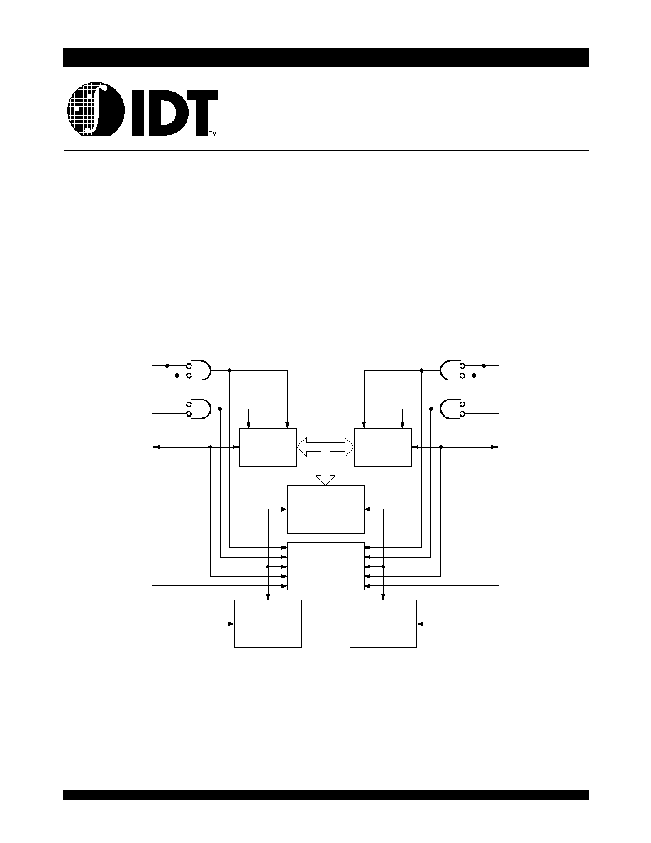
Functional Block Diagram
2721 drw 01
I/O
CONTROL
I/O
CONTROL
MEMORY
ARRAY
ADDRESS
DECODER
ADDRESS
DECODER
R/
W
R
CE
R
OE
R
I/O
0R
- I/O
7R
A
0R
- A
11R
R/
W
L
CE
L
OE
L
A
0L
- A
11L
I/O
0L
- I/O
7L
SEMAPHORE
LOGIC
SEM
R
SEM
L
x
Fully asynchronous operation from either port
x
Full on-chip hardware support of semaphore signalling be-
tween ports
x
Battery backup operation--2V data retention (LA only)
x
TTL-compatible; single 5V (±10%) power supply
x
Available in plastic packages
x
Industrial temperature range (≠40∞C to +85∞C) is available
for selected speeds
6.42
IDT71342SA/LA
High-Speed 4K x 8 Dual-Port Static RAM with Semaphore Industrial and Commercial Temperature Ranges
2
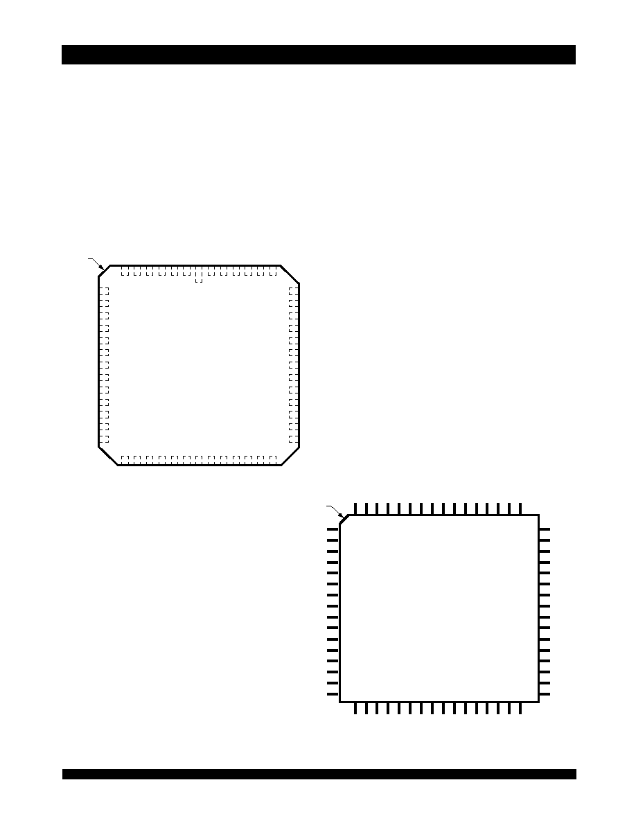
2721 drw 02
IDT71342J
J52-1
(4)
52-Pin PLCC
Top View
(5)
INDEX
N
/
C
G
N
D
I
/
O
4
L
I
/
O
5
L
I
/
O
6
L
I
/
O
7
L
I
/
O
0
R
I
/
O
1
R
I
/
O
2
R
I
/
O
3
R
I
/
O
4
R
I
/
O
5
R
I
/
O
6
R
OE
R
A
0R
A
1R
A
2R
A
3R
A
4R
A
5R
A
6R
A
7R
A
8R
A
9R
N/C
I/O
7R
46
45
44
43
42
41
40
39
38
37
36
35
34
I/O
3L
A
1L
A
2L
A
3L
A
4L
A
5L
A
6L
A
7L
A
8L
A
9L
I/O
0L
I/O
1L
I/O
2L
8
9
10
11
12
13
14
15
16
17
18
19
20
47
48
49
50
51
52
1
2
3
4
5
6
7
33
32
31
30
29
28
27
26
25
24
23
22
21
S
E
M
L
A
0
L
V
C
C
O
E
L
R
/
W
L
C
E
R
R
/
W
R
C
E
L
A
1
0
L
A
1
1
L
A
1
0
R
A
1
1
R
S
E
M
R
NOTES:
1. All Vcc pins must be connected to power supply.
2. All GND pins must be connected to ground supply.
3. J52 package body is approximately .79 in x .79 in x .17 in.
PN64 package body is approximately 14mm x 14mm x 1.4mm.
4. This package code is used to reference the package diagram.
5. This text does not indicate orientation of the actual part-marking.
Pin Configurations
(1,2,3)
INDEX
71342PF
PN64-1
(4)
64-Pin TQFP
Top View
(5)
8
9
10
11
12
13
14
15
16
1
2
3
4
5
6
7
46
45
44
43
42
41
40
39
38
37
36
35
34
47
48
33
1
7
1
8
1
9
2
0
3
2
3
1
3
0
2
9
2
8
2
7
2
6
2
5
2
4
2
3
2
2
2
1
4
9
5
0
5
1
5
2
6
3
6
2
6
1
6
0
5
9
5
8
5
7
5
6
5
5
5
4
5
3
6
4
I/O
6R
N/C
A
0R
A
1R
A
2R
A
3R
A
4R
A
5R
A
6R
A
7R
A
8R
A
9R
I/O
7R
OE
R
N/C
N/C
I/O
2L
A
0L
OE
L
A
1L
A
2L
A
3L
A
4L
A
5L
A
6L
A
7L
A
8L
A
9L
I/O
0L
I/O
1L
N/C
N/C
I
/
O
4
L
I
/
O
5
L
I
/
O
6
L
I
/
O
7
L
I
/
O
0
R
I
/
O
1
R
I
/
O
2
R
I
/
O
3
R
I
/
O
4
R
I
/
O
5
R
I
/
O
3
L
N
/
C
N
/
C
G
N
D
N
/
C
N
/
C
A
1
0
R
V
C
C
C
E
R
C
E
L
N
/
C
N
/
C
A
1
0
L
N
/
C
N
/
C
N
/
C
A
1
1
L
A
1
1
R
2721 drw 03
S
E
M
L
R
/
W
L
S
E
M
R
R
/
W
R
Description
The IDT71342 is a high-speed 4K x 8 Dual-Port Static RAM with full
on-chip hardware support of semaphore signalling between the two
ports.
The IDT71342 provides two independent ports with separate
control, address, and I/O pins that permit independent, asynchronous
access for reads or writes to any location in memory. To assist in
arbitrating between ports, a fully independent semaphore logic block
is provided. This block contains unassigned flags which can be
accessed by either side; however, only one side can control the flag at any
time. An automatic power down feature, controlled by
CE and SEM,
permits the on-chip circuitry of each port to enter a very low standby power
mode (both
CE and SEM HIGH).
Fabricated using IDT's CMOS high-performance technology, this
device typically operates on only 700mW of power. Low-power (LA)
versions offer battery backup data retention capability, with each port
typically consuming 200µW from a 2V battery. The device is packaged
in either a 64-pin TQFP or a 52-pin PLCC.

6.42
IDT71342SA/LA
High-Speed 4K x 8 Dual-Port Static RAM with Semaphore Industrial and Commercial Temperature Ranges
3
Absolute Maximum Ratings
(1)
Capacitance
(1)
(T
A
= +25∞C, f = 1.0MHz)
Maximum Operating
Temperature and Supply Voltage
(1,2)
Recommended DC Operating
Conditions
NOTES:
1. Stresses greater than those listed under ABSOLUTE MAXIMUM RATINGS may
cause permanent damage to the device. This is a stress rating only and functional
operation of the device at these or any other conditions above those indicated in the
operational sections of this specification is not implied. Exposure to absolute
maximum rating conditions for extended periods may affect reliability.
2. V
TERM
must not exceed Vcc + 10% for more than 25% of the cycle time or 10 ns
maximum, and is limited to < 20mA for the period of V
TERM
> Vcc +10%.
NOTES:
1. This parameter is determined by device characterization but is not production
tested.
2. 3dv references the interpolated capacitance when the input and output signals
switch from 0V to 3V and from 3V to 0V.
NOTES:
1. This is the parameter T
A
. This is the "instant on" case temperature.
NOTES:
1. V
IL
(min.) > -1.5V for pulse width less than 10ns.
2. V
TERM
must not exceed Vcc + 10%.
NOTE:
1. At Vcc < 2.0V input leakages are undefined.
DC Electrical Characteristics Over the Operating
Temperature and Supply Voltage
(V
CC
= 5V ± 10%)
Symbol
Rating
Commercial
& Industrial
Unit
V
TERM
(2)
Terminal Voltage
with Respect
to GND
-0.5 to +7.0
V
T
BIAS
Temperature
Under Bias
-55 to +125
o
C
T
STG
Storage
Temperature
-65 to +150
o
C
P
T
(3)
Power
Dissipation
1.5
W
I
OUT
DC Output
Current
50
mA
2721 tbl 01
Symbol
Parameter
Conditions
(2)
Max.
Unit
C
IN
Input Capacitance
V
IN
= 3dV
9
pF
C
OUT
Output Capacitance
V
OUT
= 3dV
10
pF
2721 tbl 02
Grade
Ambient
Temperature
GND
Vcc
Commercial
0
O
C to +70
O
C
0V
5.0V
+
10%
Industrial
-40
O
C to +85
O
C
0V
5.0V
+
10%
2721 tbl 03
Symbol
Parameter
Min.
Typ.
Max.
Unit
V
CC
Supply Voltage
4.5
5.0
5.5
V
GND
Ground
0
0
0
V
V
IH
Input High Voltage
2.2
____
6.0
(2)
V
V
IL
Input Low Voltage
-0.5
(1)
____
0.8
V
2721 tbl 04
Symbol
Parameter
Test Conditions
71342SA
71342LA
Unit
Min.
Max.
Min.
Max.
|I
LI
|
Input Leakage Current
(1)
V
CC
= 5.5V, V
IN
= 0V to V
CC
___
10
___
5
µ A
|I
LO
|
Output Leakage Current
CE = V
IH
, V
OUT
= 0V to V
CC
___
10
___
5
µ A
V
OL
Output Low Voltage
I
OL
= 6mA
___
0.4
___
0.4
V
I
OL
= 8mA
___
0.5
___
0.5
V
V
OH
Output High Voltage
I
OH
= -4mA
2.4
___
2.4
___
V
2721 tbl 05

6.42
IDT71342SA/LA
High-Speed 4K x 8 Dual-Port Static RAM with Semaphore Industrial and Commercial Temperature Ranges
4
DC Electrical Characteristics Over the Operating
Temperature and Supply Voltage Range
(1)
(V
CC
= 5.0V ± 10%)
NOTES:
1. 'X' in part number indicates power rating (SA or LA).
2. V
CC
= 5V, T
A
= +25∞C for typical, and parameters are not production tested.
3. f
MAX
= 1/t
RC
= All inputs cycling at f = 1/t
RC
(except Output Enable). f = 0 means no address or control lines change. Applies only to inputs at CMOS level standby I
SB3.
71342X20
Com'l Only
71342X25
Com'l & Ind
71342X35
Com'l & Ind
Symbol
Parameter
Test Condition
Version
Typ.
(2)
Max.
Typ.
(2)
Max.
Typ.
(2)
Max.
Unit
I
CC
Dynamic Operating Current
(Both Ports Active)
CE = V
IL
,
Outputs Disabled
SEM = Don't Care
f = f
MAX
(3)
COM'L
SA
LA
170
170
280
240
160
160
280
240
150
150
260
200
mA
IND
SA
LA
____
____
____
____
160
160
310
260
150
150
300
250
I
SB1
Standby Current
(Both Ports - TTL
Level Inputs)
CE
L
and
CE
R
= V
IH
SEM
L
=
SEM
R
> V
IH
f = f
MAX
(3)
COM'L
SA
LA
25
25
80
80
25
25
80
50
25
25
75
45
mA
IND
SA
LA
____
____
____
____
25
25
100
80
25
25
75
55
I
SB2
Standby Current
(One Port - TTL
Level Inputs)
CE
"A"
= V
IL
and
CE
"B"
= V
IH
Active Port Outputs Disabled,
f=f
MAX
(3)
COM'L
SA
LA
105
105
180
150
95
95
180
150
85
85
170
140
mA
IND
SA
LA
____
____
____
____
95
95
210
170
85
85
200
160
I
SB3
Full Standby Current (Both
Ports -
CMOS Level Inputs)
Both Ports
CE
L
and
CE
R
> V
CC
- 0.2V,
V
IN
> V
CC
- 0.2V or V
IN
< 0.2V
SEM
L
=
SEM
R
> V
CC
- 0.2V
f = 0
(3)
COM'L
SA
LA
1.0
0.2
15
4.5
1.0
0.2
15
4.0
1.0
0.2
15
4.0
mA
IND
SA
LA
____
____
____
____
1.0
0.2
30
10
1.0
0.2
30
10
I
SB4
Full Standby Current
(One Port -
CMOS Level Inputs)
One Port
CE
"A"
or
CE
"B"
> V
CC
- 0.2V
V
IN
> V
CC
- 0.2V or V
IN
< 0.2V
SEM
L
=
SEM
R
> V
CC
- 0.2V
Active Port Outputs Disabled,
f = f
MAX
(3)
COM'L
SA
LA
105
105
170
130
95
95
170
120
85
85
150
110
mA
IND
SA
LA
____
____
____
____
95
95
210
190
85
85
190
130
2721 tbl 06a
71342X45
Com'l Only
71342X55
Com'l & Ind
71342X70
Com'l Only
Symbol
Parameter
Test Condition
Version
Typ.
(2)
Max.
Typ.
(2)
Max.
Typ.
(2)
Max.
Unit
I
CC
Dynamic Operating Current
(Both Ports Active)
CE = V
IL
,
Outputs Disabled
SEM = Don't Care
f = f
MAX
(3)
COM'L
SA
LA
140
140
240
200
140
140
240
200
140
140
240
200
mA
IND
SA
LA
____
____
____
____
140
140
270
220
____
____
____
____
I
SB1
Standby Current
(Both Ports - TTL
Level Inputs)
CE
L
and
CE
R
= V
IH
SEM
L
=
SEM
R
> V
IH
f = f
MAX
(3)
COM'L
SA
LA
25
25
70
40
25
25
70
40
25
25
70
40
mA
IND
SA
LA
____
____
____
____
25
25
70
50
____
____
____
____
I
SB2
Standby Current
(One Port - TTL
Level Inputs)
CE
"A"
= V
IL
and
CE
"B"
= V
IH
Active Port Outputs Disabled,
f=f
MAX
(3)
COM'L
SA
LA
75
75
160
130
75
75
160
130
75
75
160
130
mA
IND
SA
LA
____
____
____
____
75
75
180
150
____
____
____
____
I
SB3
Full Standby Current (Both
Ports -
CMOS Level Inputs)
Both Ports
CE
L
and
CE
R
> V
CC
- 0.2V,
V
IN
> V
CC
- 0.2V or V
IN
< 0.2V
SEM
L
=
SEM
R
> V
CC
- 0.2
V
f = 0
(3)
COM'L
SA
LA
1.0
0.2
15
4.0
1.0
0.2
15
4.0
1.0
0.2
15
4.0
mA
IND
SA
LA
____
____
____
____
1.0
2.0
30
10
____
____
____
____
I
SB4
Full Standby Current
(One Port -
CMOS Level Inputs)
One Port
CE
"A"
or
CE
"B"
> V
CC
- 0.2V
V
IN
> V
CC
- 0.2V or V
IN
< 0.2V
SEM
L
=
SEM
R
> V
CC
- 0.2V
Active Port Outputs Disabled,
f = f
MAX
(3)
COM'L
SA
LA
75
75
150
100
75
75
150
100
75
75
150
100
mA
IND
SA
LA
____
____
____
____
75
75
170
120
____
____
____
____
2721 tbl 06b

6.42
IDT71342SA/LA
High-Speed 4K x 8 Dual-Port Static RAM with Semaphore Industrial and Commercial Temperature Ranges
5
Data Retention Characteristics
(LA Version Only) V
LC
= 0.2V, V
HC
= V
CC
- 0.2V
Data Rention Waveform
AC Test Conditions
Figure 2. Output Test Load
(for t
LZ
, t
HZ
, t
WZ
, t
OW
)
*Including scope and jig
Figure 1. AC Output Test Load
NOTES:
1. V
CC
= 2V, T
A
= +25∞C, and are not production tested.
2. t
RC
= Read Cycle Time.
3. This parameter is guaranteed by device characterization, but is not production tested.
Symbol
Parameter
Test Condition
Min.
Typ.
(1)
Max.
Unit
V
DR
V
CC
for Data Retention
___
2.0
___
V
I
CCDR
Data Retention Current
V
CC
= 2V,
CE > V
HC
COM'L. & IND.
___
100
1500
µ A
t
CDR
(3)
Chip Dese lect to Data Retention Time
SEM > V
HC
V
IN
> V
HC
or < V
LC
0
___
___
ns
t
R
(3)
Operation Recovery Time
t
RC
(2)
___
___
ns
2721 tbl 07
Input Pulse Levels
Input Rise/Fall Times
Input Timing Reference Levels
Output Reference Levels
Output Load
GND to 3.0V
5ns
1.5V
1.5V
Figures 1 and 2
2721 tbl 08
V
CC
CE
DATA RETENTION MODE
4.5V
4.5V
V
DR
>
2V
V
DR
V
IH
V
IH
t
CDR
t
R
2721 drw 04
+5V
1250
30pF
775
DATA
OUT
2721 drw 05
,
+5V
1250
5pF *
775
DATA
OUT
2721 drw 06
,