 | –≠–ª–µ–∫—Ç—Ä–æ–Ω–Ω—ã–π –∫–æ–º–ø–æ–Ω–µ–Ω—Ç: 71V016SA | –°–∫–∞—á–∞—Ç—å:  PDF PDF  ZIP ZIP |
JUNE 2002
DSC-3834/06
1
©2000 Integrated Device Technology, Inc.
Features
x
x
x
x
x
64K x 16 advanced high-speed CMOS Static RAM
x
x
x
x
x
Equal access and cycle times
-- Commercial: 10/12/15/20ns
-- Industrial: 12/15/20ns
x
x
x
x
x
One Chip Select plus one Output Enable pin
x
x
x
x
x
Bidirectional data inputs and outputs directly
LVTTL-compatible
x
x
x
x
x
Low power consumption via chip deselect
x
x
x
x
x
Upper and Lower Byte Enable Pins
x
x
x
x
x
Single 3.3V power supply
x
x
x
x
x
Available in 44-pin Plastic SOJ, 44-pin TSOP, and
48-Ball Plastic FBGA packages
Description
The IDT71V016 is a 1,048,576-bit high-speed Static RAM organized
as 64K x 16. It is fabricated using IDT's high-perfomance, high-reliability
CMOS technology. This state-of-the-art technology, combined with inno-
vative circuit design techniques, provides a cost-effective solution for high-
speed memory needs.
The IDT71V016 has an output enable pin which operates as fast
as 5ns, with address access times as fast as 10ns. All bidirectional
inputs and outputs of the IDT71V016 are LVTTL-compatible and operation
is from a single 3.3V supply. Fully static asynchronous circuitry is used,
requiring no clocks or refresh for operation.
The IDT71V016 is packaged in a JEDEC standard 44-pin Plastic
SOJ, a 44-pin TSOP Type II, and a 48-ball plastic 7 x 7 mm FBGA.
Functional Block Diagram
Output
Enable
Buffer
Address
Buffers
Chip
Enable
Buffer
Write
Enable
Buffer
Byte
Enable
Buffers
OE
A
0
≠ A
15
Row / Column
Decoders
CS
WE
BHE
BLE
64K x 16
Memory
Array
Sense
Amps
and
Write
Drivers
16
Low
Byte
I/O
Buffer
8
8
8
8
I/O
8
I/O
15
I/O
7
I/O
0
3834 drw 01
High
Byte
I/O
Buffer
3.3V CMOS Static RAM
1 Meg (64K x 16-Bit)
IDT71V016SA
6.42
2
IDT71V016SA, 3.3V CMOS Static RAM
1 Meg (64K x 16-Bit) Commercial and Industrial Temperature Ranges
1
2
3
4
5
6
A
BLE
OE
A
0
A
1
A
2
NC
B
I/O
8
BHE
A
3
A
4
CS
I/O
0
C
I/O
9
I/O
10
A
5
A
6
I/O
1
I/O
2
D
V
SS
I/O
11
NC
A
7
I/O
3
V
DD
E
V
DD
I/O
12
NC
NC
I/O
4
V
SS
F
I/O
14
I/O
13
A
14
A
15
I/O
5
I/O
6
G
I/O
15
NC
A
12
A
13
WE
I/O
7
H
NC
A
8
A
9
A
10
A
11
NC
3834 tbl 02a
Pin Configurations
SOJ/TSOP
Top View
Pin Description
Truth Table
(1)
1
2
3
4
5
6
7
8
9
10
11
12
13
14
15
16
17
18
19
20
21
22
I/O
7
NC
A
12
A
13
A
14
A
15
WE
I/O
6
I/O
5
I/O
4
V
SS
V
DD
I/O
3
I/O
2
I/O
1
I/O
0
CS
A
0
A
1
A
2
A
3
A
4
44
43
42
41
40
39
38
37
36
35
34
33
32
31
30
29
28
27
26
25
24
23
A
6
A
7
OE
BHE
BLE
I/O
15
I/O
14
I/O
13
I/O
12
V
SS
V
DD
I/O
11
I/O
10
I/O
9
I/O
8
A
8
A
9
A
10
A
11
NC
A
5
NC
SO44-1
SO44-2
3834 drw 02
NOTE:
1. H = V
IH
, L = V
IL
, X = Don't care.
A
0
≠ A
15
Address Inputs
Input
CS
Chip Select
Input
WE
Write Enable
Input
OE
Output Enable
Input
BHE
High Byte Enable
Input
BLE
Low Byte Enable
Input
I/O
0
≠ I/O
15
Data Input/Output
I/O
V
DD
3.3V Power
Power
V
SS
Ground
Gnd
3834 tbl 01
CS
OE
WE
BLE
BHE
I/O
0
-I/O
7
I/O
8
-I/O
15
Function
H
X
X
X
X
High-Z
High-Z
Deselected ≠ Standby
L
L
H
L
H
DATA
OUT
High-Z
Low Byte Read
L
L
H
H
L
High-Z
DATA
OUT
High Byte Read
L
L
H
L
L
DATA
OUT
DATA
OUT
Word Read
L
X
L
L
L
DATA
IN
DATA
IN
Word Write
L
X
L
L
H
DATA
IN
High-Z
Low Byte Write
L
X
L
H
L
High-Z
DATA
IN
High Byte Write
L
H
H
X
X
High-Z
High-Z
Outputs Disabled
L
X
X
H
H
High-Z
High-Z
Outputs Disabled
3834 tbl 02
FBGA (BF48-1)
Top View
6.42
3
IDT71V016SA, 3.3V CMOS Static RAM
1 Meg (64K x 16-Bit) Commercial and Industrial Temperature Ranges
Symbol
Parameter
71V016SA10
71V016SA12
71V016SA15
71V016SA20
Unit
Com'l Only
Com'l
Ind
Com'l
Ind
Com'l
Ind
I
CC
Dynamic Operating Current
CS
V
LC
, Outputs Open, V
DD
= Max., f = f
MAX
(3)
Max.
160
150
160
130
130
120
120
mA
Typ.
(4)
125
120
--
110
--
110
--
I
SB
Dynamic Standby Power Supply Current
CS
V
HC
, Outputs Open, V
DD
= Max., f = f
MAX
(3)
45
40
45
35
35
30
30
mA
I
SB1
Full Standby Power Supply Current (static)
CS
V
HC
, Outputs Open, V
DD
= Max., f = 0
(3)
10
10
10
10
10
10
10
mA
3834 tbl 08
Absolute Maximum Ratings
(1)
Recommended Operating
Temperature and Supply Voltage
DC Electrical Characteristics
(V
DD
= Min. to Max., Commercial and Industrial Temperature Ranges)
Capacitance
(T
A
= +25∞C, f = 1.0MHz, SOJ package)
Recommended DC Operating
Conditions
DC Electrical Characteristics
(1,2)
(V
DD
= Min. to Max., V
LC
= 0.2V, V
HC
= V
DD
≠ 0.2V)
NOTE:
1. Stresses greater than those listed under ABSOLUTE MAXIMUM RATINGS may cause
permanent damage to the device. This is a stress rating only and functional operation
of the device at these or any other conditions above those indicated in the operational
sections of this specification is not implied. Exposure to absolute maximum rating
conditions for extended periods may affect reliability.
NOTES:
1. For 71V016SA10 only.
2. For all speed grades except 71V016SA10.
3. V
IH
(max.) = V
DD
+2V for pulse width less than 5ns, once per cycle.
4. V
IL
(min.) = ≠2V for pulse width less than 5ns, once per cycle.
NOTE:
1. This parameter is guaranteed by device characterization, but not production tested.
NOTES:
1. All values are maximum guaranteed values.
2. All inputs switch between 0.2V (Low) and V
DD
≠ 0.2V (High).
3. f
MAX
= 1/t
RC
(all address inputs are cycling at f
MAX
); f = 0 means no address input lines are changing
.
4. Typical values are measured at 3.3V, 25∞C and with equal read and write cycles.
Symbol
Rating
Value
Unit
V
DD
Supply Voltage Relative to
V
SS
≠0.5 to +4.6
V
V
IN
, V
OUT
Terminal Voltage Relative
to V
SS
≠0.5 to V
DD
+0.5
V
T
BIAS
Temperature Under Bias
≠55 to +125
o
C
T
STG
Storage Temperature
≠55 to +125
o
C
P
T
Power Dissipation
1.25
W
I
OUT
DC Output Current
50
mA
3834 tbl 03
Grade
Temperature
V
SS
V
DD
Commercial
0∞C to +70∞C
0V
See Below
Industrial
-40∞C to +85∞C
0V
See Below
3834 tbl 04
Symbol
Parameter
Min.
Typ.
Max.
Unit
V
DD
(1)
Supply Voltage
3.15
3.3
3.6
V
V
DD
(2)
Supply Voltage
3.0
3.3
3.6
V
Vss
Ground
0
0
0
V
V
IH
Input High Voltage
2.0
____
V
DD
+0.3
(3)
V
V
IL
Input Low Voltage
≠0.3
(4)
____
0.8
V
3834 tbl 05
Symbol
Parameter
(1)
Conditions
Max.
Unit
C
IN
Input Capacitance
V
IN
= 3dV
6
pF
C
I/O
I/O Capacitance
V
OUT
= 3dV
7
pF
3834 tbl 06
Symbol
Parameter
Test Condition
IDT71V016SA
Unit
Min.
Max.
|I
LI
|
Input Leakage Current
V
DD
= Max., V
IN
= V
SS
to V
DD
___
5
µ A
|I
LO
|
Output Leakage Current
V
DD
= Max.,
CS = V
IH
, V
OUT
= V
SS
to V
DD
___
5
µ A
V
OL
Output Low Voltage
I
OL
= 8mA, V
DD
= Min.
___
0.4
V
V
OH
Output High Voltage
I
OH
= ≠4mA, V
DD
= Min.
2.4
___
V
3834 tbl 07
6.42
4
IDT71V016SA, 3.3V CMOS Static RAM
1 Meg (64K x 16-Bit) Commercial and Industrial Temperature Ranges
AC Test Conditions
AC Test Loads
Figure 3. Output Capacitive Derating
Figure 1. AC Test Load
Figure 2. AC Test Load
(for t
CLZ
, t
OLZ
, t
CHZ
, t
OHZ
, t
OW,
and t
WHZ
)
*Including jig and scope capacitance.
+1.5V
50
I/O
Z
0
= 50
3834 drw 03
30pF
3834 drw 04
320
350
5pF*
DATA
OUT
3.3V
1
2
3
4
5
6
7
20
40
60 80 100 120 140 160 180 200
t
AA,
t
ACS
(Typical, ns)
CAPACITANCE (pF)
8
3834 drw 05
∑
∑
∑
∑
∑
∑
∑
Input Pulse Levels
Input Rise/Fall Times
Input Timing Reference Levels
Output Reference Levels
AC Test Load
GND to 3.0V
1.5ns
1.5V
1.5V
See Figure 1, 2 and 3
3834 tbl 09
6.42
5
IDT71V016SA, 3.3V CMOS Static RAM
1 Meg (64K x 16-Bit) Commercial and Industrial Temperature Ranges
71V016SA10
(2)
71V016SA12
71V016SA15
71V016SA20
Symbol
Parameter
Min.
Max.
Min.
Max.
Min.
Max.
Min.
Max.
Unit
READ CYCLE
t
RC
Read Cycle Time
10
____
12
____
15
____
20
____
ns
t
AA
Address Access Time
____
10
____
12
____
15
____
20
ns
t
ACS
Chip Select Access Time
____
10
____
12
____
15
____
20
ns
t
CLZ
(1)
Chip Select Low to Output in Low-Z
4
____
4
____
5
____
5
____
ns
t
CHZ
(1)
Chip Select High to Output in High-Z
____
5
____
6
____
6
____
8
ns
t
OE
Outp ut Enable Low to Output Valid
____
5
____
6
____
7
____
8
ns
t
OLZ
(1)
Output Enable Low to Output in Low-Z
0
____
0
____
0
____
0
____
ns
t
OHZ
(1)
Output Enable High to Output in High-Z
____
5
____
6
____
6
____
8
ns
t
OH
Output Hold from Address Change
4
--
4
--
4
--
4
--
ns
t
BE
Byte Enable Low to Output Valid
--
5
--
6
--
7
____
8
ns
t
BLZ
(1)
Byte Enable Low to Output in Low-Z
0
____
0
____
0
____
0
____
ns
t
BHZ
(1)
Byte Enable High to Output in High-Z
____
5
____
6
____
6
____
8
ns
WRITE CYCLE
t
WC
Write Cycle Time
10
____
12
____
15
____
20
____
ns
t
AW
Address Valid to End of Write
7
____
8
____
10
____
12
____
ns
t
CW
Chip Select Lo w to End of Write
7
____
8
____
10
____
12
____
ns
t
BW
Byte Enable Lo w to End of Write
7
____
8
____
10
____
12
____
ns
t
AS
Address Set-up Time
0
____
0
____
0
____
0
____
ns
t
WR
Ad dress Hold from End of Write
0
____
0
____
0
____
0
____
ns
t
WP
Write Pulse Width
7
____
8
____
10
____
12
____
ns
t
DW
Data Valid to End of Write
5
____
6
____
7
____
9
____
ns
t
DH
Data Hold Time
0
____
0
____
0
____
0
____
ns
t
OW
(1)
Write Enable High to Output in Low-Z
3
____
3
____
3
____
3
____
ns
t
WHZ
(1)
Write Enable Low to Output in High-Z
____
5
____
6
____
6
____
8
ns
3834 tbl 10
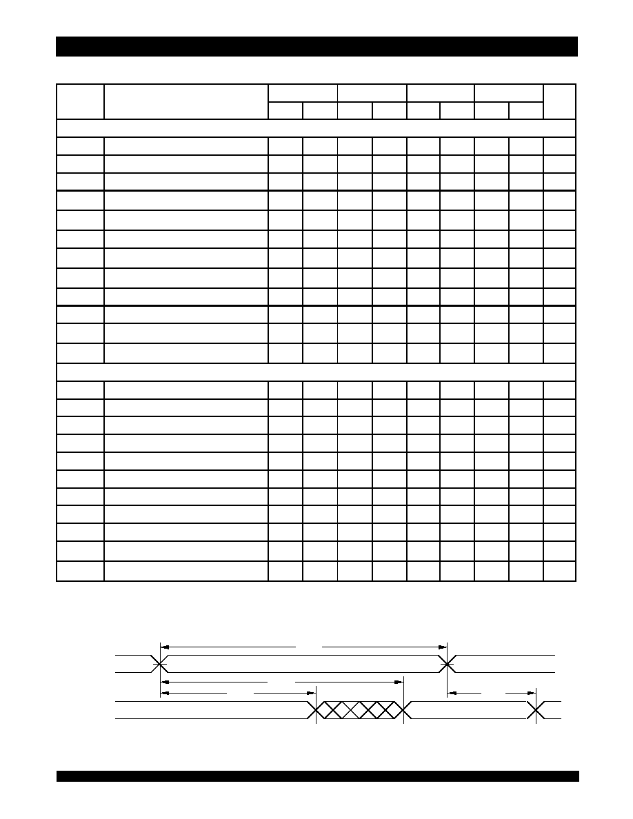
Timing Waveform of Read Cycle No. 1
(1,2,3)
NOTES:
1.
WE is HIGH for Read Cycle.
2. Device is continuously selected,
CS is LOW.
3.
OE, BHE, and BLE are LOW.
AC Electrical Characteristics
(V
DD
= Min. to Max., Commercial and Industrial Temperature Ranges)
DATA
OUT
ADDRESS
3834 drw 06
t
RC
t
AA
t
OH
t
OH
DATA
OUT
VALID
PREVIOUS DATA
OUT
VALID
NOTES:
1. This parameter is guaranteed with the AC Load (Figure 2) by device characterization, but is not production tested.
2. 0
∞
C to +70
∞
C temperature range only.