 | –≠–ª–µ–∫—Ç—Ä–æ–Ω–Ω—ã–π –∫–æ–º–ø–æ–Ω–µ–Ω—Ç: 71V30 | –°–∫–∞—á–∞—Ç—å:  PDF PDF  ZIP ZIP |
©2000 Integrated Device Technology, Inc.
JANUARY 2001
DSC 3741/7
1
HIGH-SPEED 3.3V
1K X 8 DUAL-PORT
STATIC RAM
IDT71V30S/L
Features
x
High-speed access
≠ Commercial: 25/35/55ns (max.)
x
Low-power operation
≠ IDT71V30S
--
Active: 375mW (typ.)
--
Standby: 5mW (typ.)
≠ IDT71V30L
--
Active: 375mW (typ.)
--
Standby: 1mW (typ.)
Functional Block Diagram
NOTES:
1.
IDT71V30:
BUSY outputs are non-tristatable push-pulls.
2.
INT outputs are non-tristable push-pull output structure.
x
On-chip port arbitration logic
x
Interrupt flags for port-to-port communication
x
Fully asynchronous operation from either port
x
Battery backup operation, 2V data retention (L Only)
x
TTL-compatible, single 3.3V ±0.3V power supply
x
Industrial temperature range (-40
O
C to +85
O
C) is available
for selected speeds
I/O
Control
Address
Decoder
MEMORY
ARRAY
ARBITRATION
and
INTERRUPT
LOGIC
Address
Decoder
I/O
Control
R/
W
L
CE
L
OE
L
BUSY
L
A
9L
A
0L
3741 drw 01
I/O
0L
- I/O
7L
CE
L
OE
L
R/
W
L
INT
L
BUSY
R
I/O
0R
-I/O
7R
A
9R
A
0R
INT
R
CE
R
OE
R
(2)
(1)
(1)
(2)
R/
W
R
CE
R
OE
R
10
10
R/
W
R
6.42
IDT71V30S/L
High-Speed 1K x 8 Dual-Port Static RAM with Interrupts Industrial and Commercial Temperature Ranges
2
NOTES:
1. All V
CC
pins must be connected to the power supply.
2. All GND pins must be connected to the ground supply.
3. Package body is approximately 10mm x 10mm x 1.4mm.
4. This package code is used to reference the package diagram.
5. This text does not indicate the orientation of the actual part-marking.
Pin Configurations
(1,2,3)
Description
The IDT71V30 is a high-speed 1K x 8 Dual-Port Static RAM. The
IDT71V30 is designed to be used as a stand-alone 8-bit Dual-Port
SRAM.
Both devices provide two independent ports with separate control,
address, and I/O pins that permit independent, asynchronous access
for reads or writes to any location in memory. An automatic power
down feature, controlled by
CE, permits the on chip circuitry of each
port to enter a very low standby power mode.
Fabricated using IDT's CMOS high-performance technology, these
devices typically operate on only 375mW of power. Low-power (L)
versions offer battery backup data retention capability, with each Dual-
Port typically consuming 200µW from a 2V battery.
The IDT71V30 devices are packaged in 64-pin STQFPs.
INDEX
IDT71V30TF
PP64-1
(4)
64-Pin STQFP
Top View
(5)
8
9
10
11
12
13
14
15
16
1
2
3
4
5
6
7
46
45
44
43
42
41
40
39
38
37
36
35
34
47
48
33
1
7
1
8
1
9
2
0
3
2
3
1
3
0
2
9
2
8
2
7
2
6
2
5
2
4
2
3
2
2
2
1
4
9
5
0
5
1
5
2
6
3
6
2
6
1
6
0
5
9
5
8
5
7
5
6
5
5
5
4
5
3
6
4
I/O
6R
N/C
A
0R
A
1R
A
2R
A
3R
A
4R
A
5R
A
6R
A
7R
A
8R
A
9R
I/O
7R
OE
R
N/C
N/C
I/O
2L
A
0L
OE
L
A
1L
A
2L
A
3L
A
4L
A
5L
A
6L
A
7L
A
8L
A
9L
I/O
0L
I/O
1L
N/C
N/C
3741 drw 03
N
/
C
N
/
C
N
/
C
I
N
T
L
B
U
S
Y
L
R
/
W
L
C
E
L
V
C
C
V
C
C
C
E
R
R
/
W
R
B
U
S
Y
R
I
N
T
R
N
/
C
N
/
C
N
/
C
I
/
O
3
L
N
/
C
I
/
O
4
L
I
/
O
5
L
I
/
O
6
L
I
/
O
7
L
N
/
C
G
N
D
G
N
D
I
/
O
0
R
I
/
O
1
R
I
/
O
2
R
I
/
O
3
R
N
/
C
I
/
O
4
R
I
/
O
5
R
,
6.42
IDT71V30S/L
High-Speed 1K x 8 Dual-Port Static RAM with Interrupts Industrial and Commercial Temperature Ranges
3
Absolute Maximum Ratings
(1)
Recommended
DC Operating Conditions
Maximum Operating
Temperature and Supply Voltage
(1,2)
DC Electrical Characteristics Over the
Operating Temperature and Supply Voltage Range
(V
CC
= 3.3V ± 0.3V)
NOTES:
1.
Stresses greater than those listed under ABSOLUTE MAXIMUM RATINGS
may cause permanent damage to the device. This is a stress rating only
and functional operation of the device at these or any other conditions above
those indicated in the operational sections of the specification is not implied.
Exposure to absolute maximum rating conditions for extended periods may
affect reliability.
2.
V
TERM
must not exceed Vcc + 0.3V for more than 25% of the cycle time or 10ns
maximum, and is limited to < 20mA for the period of V
TERM
> Vcc + 0.3V.
NOTE:
1.
V
IL
(min.) = -1.5V for pulse width less than 20ns.
NOTE:
1. At Vcc < 2.0V input leakages are undefined.
Supply CurrentV
IN
> V
CC
-0.2V or < 0.2V
Capacitance
(1)
(T
A
= +25
O
C, f=1.0MHz)
NOTES:
1. This parameter is determined by device characterization but is not production
tested.
2. 3dv references the interpolated capacitance when the input and output signals
switch from 0V to 3V or from 3V to 0V.
NOTES:
1. This is the parameter T
A
. This is the "instant on" case temperature.
2.
Industrial temperature: for specific speeds, packages and powers,
contact your sales office.
Symbol
Rating
Com'l & Ind
Unit
V
TERM
(2)
Terminal Voltage
with Respect to GND
-0.5 to +4.60
V
T
BIAS
Temperature
Under Bias
-55 to +125
o
C
T
STG
Storage
Temperature
-65 to +150
o
C
I
OUT
DC Output
Current
50
mA
3741 tbl 01
Symbol
Parameter
Min.
Typ.
Max.
Unit
V
CC
Supply Voltage
3.0
3.3
3.6
V
GND
Ground
0
0
0
V
V
IH
Input High Voltage
2.0
____
V
CC
+
0.3V
V
V
IL
Input Low Voltage
-0.3
(1)
____
0.8
V
3741 tbl 02
Grade
Ambient
Temperature
GND
Vcc
Commercial
0
O
C to +70
O
C
0V
3.3V
+
0.3
Industrial
-40
O
C to +85
O
C
0V
3.3V
+
0.3
3741 tbl 03
Symbol
Parameter
Conditions
(2)
Max.
Unit
C
IN
Input Capacitance
V
IN
= 3dV
9
pF
C
OUT
Output
Capacitance
V
OUT
= 3dV
10
pF
3741 tbl 04
Symbol
Parameter
Test Conditions
71V30S
71V30L
Unit
Min.
Max.
Min.
Max.
|I
LI
|
Input Leakage
Current
(1)
V
CC
= 3.6V,
V
IN
= 0V to V
CC
___
10
___
5
µ A
|I
LO
|
Output Leakage
Current
CE = V
IH
,
V
OUT
= 0V to V
CC
___
10
___
5
µ A
V
OL
Output Low Voltage
(I/O
0
-I/O
7
)
I
OL
= 4mA
___
0.4
___
0.4
V
V
OH
Output High Voltage
I
OH
= -4mA
2.4
___
2.4
___
V
3741 tbl 05
6.42
IDT71V30S/L
High-Speed 1K x 8 Dual-Port Static RAM with Interrupts Industrial and Commercial Temperature Ranges
4
NOTES:
1. V
CC
= 2V, T
A
= +25∞C, and is not production tested.
2. t
RC
= Read Cycle Time.
3. This parameter is guaranteed by device characterization but not production tested.
Data Retention Characteristics
(L Version Only)
DC Electrical Characteristics Over the Operating
Temperature and Supply Voltage Range
(1,6,7)
(V
CC
= 3.3V ± 0.3V)
NOTES:
1.
'X' in part number indicates power rating (S or L)
2.
V
CC
= 3.3V, T
A
= +25∞C, and are not production tested. I
CCDC
= 70mA (Typ.)
3.
At f = f
MAX
,
address and control lines (except Output Enable) are cycling at the maximum frequency read cycle of 1/t
RC.
4.
f = 0 means no address or control lines change.
5.
Port "A" may be either left or right port. Port "B" is the opposite from port "A".
6.
Refer to chip enable Truth Table I.
7.
Industrial temperature: for specific speeds, packages and powers contact your sales office.
Symbol
Parameter
Test Condition
Version
71V30X25
Com'l Only
71V30X35
Com'l Only
71V30X55
Com'l Only
Unit
Typ.
(2)
Max.
Typ.
(2)
Max.
Typ.
(2)
Max.
I
CC
Dynamic Operating Current
(Both Ports Active)
CE
L
and
CE
R
= V
IL
,
Outputs Disabled
f = f
MAX
(3)
COM'L
S
L
75
75
150
120
75
75
145
115
75
75
135
105
mA
IND
S
L
___
___
___
___
___
___
___
___
___
___
___
___
I
SB1
Standby Current
(Both Ports - TTL Level
Inputs)
CE
L
and
CE
R
= V
IL
,
f = f
MAX
(3)
COM'L
S
L
20
20
50
35
20
20
50
35
20
20
50
35
mA
IND
S
L
___
___
___
___
___
___
___
___
___
___
___
___
I
SB2
Standby Current
(One Port - TTL Level
Inputs)
CE
"A"
= V
IL
and CE
"B"
= V
IH
(5)
Active Port Outputs Disabled,
f=f
MAX
(3)
COM'L
S
L
30
30
105
75
30
30
100
70
30
30
90
60
mA
IND
S
L
___
___
___
___
___
___
___
___
___
___
___
___
I
SB3
Full Standby Current (Both
Ports - CMOS Level Inputs)
CE
L
and CE
R
> V
CC
- 0.2V
V
IN
> V
CC
- 0.2V or
V
IN
< 0.2V, f = 0
(4)
COM'L
S
L
1.0
0.2
5.0
3.0
1.0
0.2
5.0
3.0
1.0
0.2
5.0
3.0
mA
IND
S
L
___
___
___
___
___
___
___
___
___
___
___
___
I
SB4
Full Standby Current
(One Port - CMOS
Level Inputs)
CE
"A"
< 0.2V and
CE
"B"
> V
CC
- 0.2V
(5)
V
IN
> V
CC
- 0.2V or V
IN
< 0.2V
Active Port Outputs Disabled
f=f
MAX
(3)
COM'L
S
L
30
30
90
75
30
30
85
70
30
30
75
60
mA
IND
S
L
___
___
___
___
___
___
___
___
___
___
___
___
3741 tbl 06
Symbol
Parameter
Test Condition
71V30L
Unit
Min.
Typ.
(1)
Max.
V
DR
V
CC
for Data Retention
2.0
____
____
V
I
CCDR
Data Retention Current
V
CC
= 2
V,
CE > V
CC
-0.2V
Ind.
____
____
____
µ A
Com'l.
____
100
1500
t
CDR
(3)
Chip Deselect to Data Retention Time
V
IN
> V
CC
-0.2V or V
IN
< 0.2V
0
____
____
ns
t
R
(3)
Operation Recovery Time
t
RC
(2)
____
____
ns
3741 tbl 07
6.42
IDT71V30S/L
High-Speed 1K x 8 Dual-Port Static RAM with Interrupts Industrial and Commercial Temperature Ranges
5
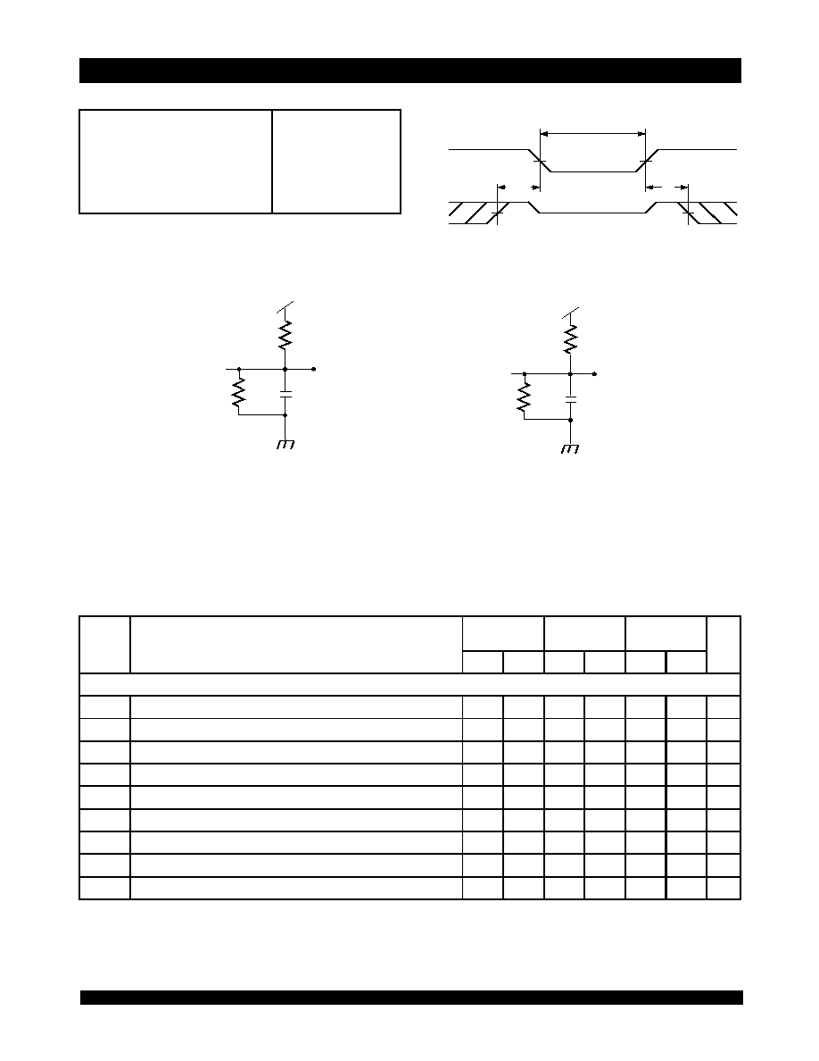
AC Test Conditions
Data Retention Waveform
NOTES:
1. Transition is measured 0mV from Low- or High-impedance voltage with Output Test Load (Figure 2).
2.
This parameter is guaranteed by device characterization, but is not production tested.
3.
'X' in part number indicates power rating (S or L).
4.
Industrial temperature: for specific speeds, packages and power contact your sales office.
Figure 2. Output Test Load
(For t
HZ
, t
LZ
, t
WZ
and t
OW
)
* Including scope and jig.
Figure 1. AC Output Test Load
AC Electrical Characteristics Over the
Operating Temperature and Supply Voltage Range
(3,4)
Input Pulse Levels
Input Rise/Fall Times
Input Timing Reference Levels
Output Reference Levels
Output Load
GND to 3.0V
3ns Max.
1.5V
1.5V
Figures 1 and 2
3741 tbl 08
V
CC
CE
3.0V
3.0V
DATA RETENTION MODE
t
CDR
V
IH
V
IH
V
DR
V
DR
2.0V
3741 drw 04
t
R
,
590
30pF
435
DATA
OUT
590
435
5pF
DATA
OUT
3741 drw 05
3.3V
3.3V
BUSY
INT
71V30X25
Com'l Only
71V30X35
Com'l Only
71V30X55
Com'l Only
Unit
Symbol
Parameter
Min.
Max.
Min.
Max.
Min.
Max.
READ CYCLE
t
RC
Read Cycle Time
25
____
35
____
55
____
ns
t
AA
Address Access Time
____
25
____
35
____
55
ns
t
ACE
Chip Enable Access Time
____
25
____
35
____
55
ns
t
AOE
Output Enable Access Time
____
12
____
20
____
25
ns
t
OH
Output Hold from Address Change
3
____
3
____
3
____
ns
t
LZ
Output Low-Z Time
(1,2)
0
____
0
____
0
____
ns
t
HZ
Output High-Z Time
(1,2)
____
12
____
15
____
30
ns
t
PU
Chip Enable to Power Up Time
(2)
0
____
0
____
0
____
ns
t
PD
Chip Disable to Power Down Time
(2)
____
50
____
50
____
50
ns
3741 tbl 09