JANUARY 2002
DSC-5281/07
1
©2002 Integrated Device Technology, Inc.
Pin Description Summary
Description
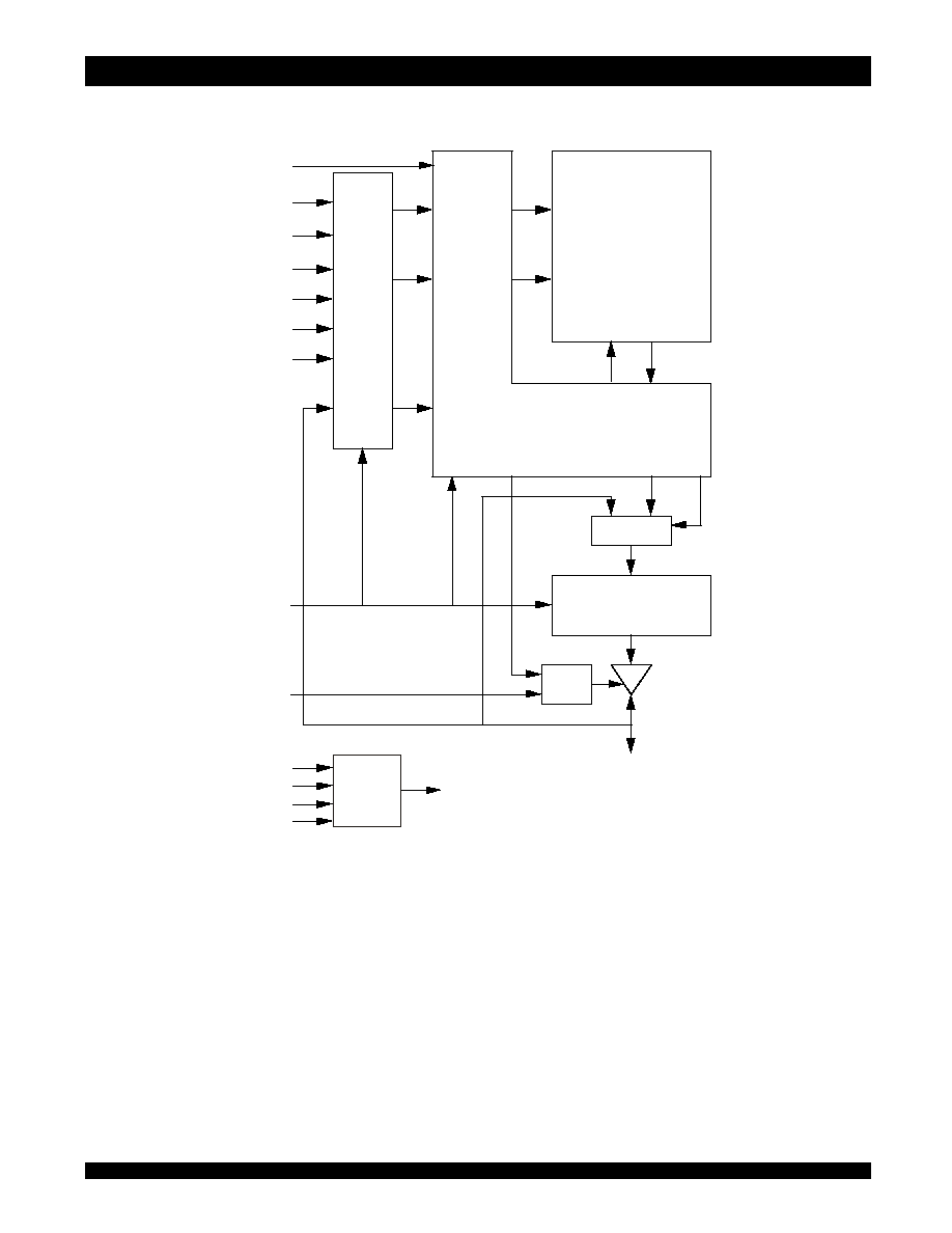
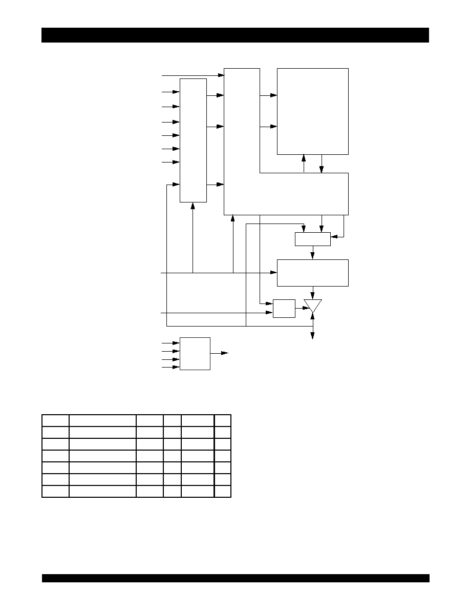
The IDT71V3556/58 are 3.3V high-speed 4,718,592-bit (4.5 Mega-
bit) synchronous SRAMS. They are designed to eliminate dead bus
cycles when turning the bus around between reads and writes, or
writes and reads. Thus, they have been given the name ZBT
TM
, or
Zero Bus Turnaround.
Address and control signals are applied to the SRAM during one
clock cycle, and two cycles later the associated data cycle occurs, be it
read or write.
The IDT71V3556/58 contain data I/O, address and control signal
registers. Output enable is the only asynchronous signal and can be used
to disable the outputs at any given time.
A Clock Enable (
CEN) pin allows operation of the IDT71V3556/58
to be suspended as long as necessary. All synchronous inputs are
ignored when (
CEN) is high and the internal device registers will hold
their previous values.
There are three chip enable pins (
CE
1
, CE
2
,
CE
2
) that allow the user
to deselect the device when desired. If any one of these three are not
asserted when ADV/
LD is low, no new memory operation can be
initiated. However, any pending data transfers (reads or writes) will be
completed. The data bus will tri-state two cycles after chip is deselected
or a write is initiated.
Features
x
x
x
x
x
128K x 36, 256K x 18 memory configurations
x
x
x
x
x
Supports high performance system speed - 200 MHz
(3.2 ns Clock-to-Data Access)
x
x
x
x
x
ZBT
TM
Feature - No dead cycles between write and read
cycles
x
x
x
x
x
Internally synchronized output buffer enable eliminates the
need to control
OE
x
x
x
x
x
Single R/
W (READ/WRITE) control pin
x
x
x
x
x
Positive clock-edge triggered address, data, and control
signal registers for fully pipelined applications
x
x
x
x
x
4-word burst capability (interleaved or linear)
x
x
x
x
x
Individual byte write (
BW
1
-
BW
4
) control (May tie active)
x
x
x
x
x
Three chip enables for simple depth expansion
x
x
x
x
x
3.3V power supply (±5%), 3.3V I/O Supply (V
DDQ)
x
x
x
x
x
Optional- Boundary Scan JTAG Interface (IEEE 1149.1
compliant)
x
x
x
x
x
Packaged in a JEDEC standard 100-pin plastic thin quad
flatpack (TQFP), 119 ball grid array (BGA) and 165 fine pitch
ball grid array (fBGA)
A
0
-A
17
Address Inputs
Input
Synchronous
CE
1
, CE
2
,
CE
2
Chip Enables
Input
Synchronous
OE
Output Enable
Input
Asynchronous
R/
W
Read/Write Signal
Input
Synchronous
CEN
Clock Enable
Input
Synchronous
BW
1
,
BW
2
,
BW
3
,
BW
4
Individual Byte Write Selects
Input
Synchronous
CLK
Clock
Input
N/A
ADV/
LD
Advance b urst address / Load new address
Input
Synchronous
LBO
Linear / Interleaved Burst Order
Input
Static
TMS
Test Mode Select
Input
Synchronous
TDI
Test Data Input
Input
Synchronous
TCK
Test Clock
Input
N/A
TDO
Test Data Output
Output
Synchronous
TRST
JTAG Reset (Optional)
Input
Asynchronous
ZZ
Sleep Mode
Input
Synchronous
I/O
0
-I/O
31
, I/O
P1
-I/O
P4
Data Input / Output
I/O
Synchronous
V
DD
, V
DDQ
Core Power, I/O Power
Supply
Static
V
SS
Ground
Supply
Static
5281 tbl 01
IDT71V3556S
IDT71V3558S
IDT71V3556SA
IDT71V3558SA
128K x 36, 256K x 18
3.3V Synchronous ZBT SRAMs
3.3V I/O, Burst Counter
Pipelined Outputs
6.42
2
IDT71V3556, IDT71V3558, 128K x 36, 256K x 18, 3.3V Synchronous SRAMS with
ZBT
TM
TM
TM
TM
TM
Feature, 3.3V I/O, Burst Counter, and Pipelined Outputs Commercial and Industrial Temperature Ranges
Pin Definition
(1)
NOTE:
1. All synchronous inputs must meet specified setup and hold times with respect to CLK.
Symbol
Pin Function
I/O
Active
Description
A
0
-A
17
Address Inputs
I
N/A
Synchronous Address inputs. The address register is triggered by a combination of the rising edge of CLK,
ADV/
LD low, CEN low, and true chip enables.
ADV/
LD
Advance / Load
I
N/A
ADV/
LD is a synchronous input that is used to load the internal registers with new address and control when it
is sampled low at the rising edge of clock with the chip selected. When ADV/
LD is low with the chip
deselected, any burst in progress is terminated. When ADV/
LD is sampled high then the internal burst counter
is advanced for any burst that was in progress. The external addresses are ignored when ADV/
LD is sampled
high.
R/
W
Read / Write
I
N/A
R/
W signal is a synchronous input that identifies whether the current load cycle initiated is a Read or Write
access to the memory array. The data bus activity for the current cycle takes place two clock cycles later.
CEN
Clock Enable
I
LOW
Sync hronous Clock Enable Input. When
CEN is sampled high, all other synchronous inputs, including clock are
ignored and outputs remain unchanged. The effect of
CEN sampled high on the device outputs is as if the low
to high clock transition did not occur. For normal operation,
CEN must be sampled low at rising edge of clock.
BW
1
-
BW
4
Individual Byte
Write Enables
I
LOW
Synchronous byte write enables. Each 9-bit b yte has its own active low byte write enable. On load write cycles
(When R/
W and ADV/LD are sampled low) the appropriate byte write signal (BW
1
-
BW
4
) must be valid. The byte
write signal must also be valid on each cycle of a burst write. Byte Write signals are ignored when R/
W is
sampled high. The appropriate byte(s) of data are written into the de vice two cycles later.
BW
1
-
BW
4
can all be
tied low if always doing write to the entire 36-bit word.
CE
1
,
CE
2
Chip Enables
I
LOW
S ynchronous active low chip enable.
CE
1
and
CE
2
are used with CE
2
to enable the IDT71V3556/58. (
CE
1
or
CE
2
sampled high or CE
2
sampled low) and ADV/
LD low at the rising edge of clock, initiates a deselect cycle.
The ZBT
TM
has a two cycle deselect, i.e., the data bus will tri-state two clo ck cycles after deselect is initiated.
CE
2
Chip Enable
I
HIGH
Sync hronous active high chip enable. CE
2
is used with
CE
1
and
CE
2
to enable the chip. CE
2
has inverted
polarity but otherwise identical to
CE
1
and
CE
2
.
CLK
Clock
I
N/A
This is the clock input to the IDT71V3556/58. Except for
OE, all timing references for the device are made with
respect to the rising edge of CLK.
I/O
0
-I/O
31
I/O
P1
-I/O
P4
Data Input/Output
I/O
N/A
Synchronous data input/output (I/O) pins . Both the data input path and data output path are registered and
triggered by the rising edge of CLK.
LBO
Linear Burst Order
I
LOW
Burst order selection input. When
LBO is high the Interleaved burst sequence is selected. When LBO is low
the Linear burst sequence is selected.
LBO is a static input and it must not change during device operation.
OE
Output Enable
I
LOW
Asynchronous output enable.
OE must be low to read data from the 71V3556/58. When OE is high the I/O pins
are in a high-impedance state.
OE does not need to be actively controlled for read and write cycles. In normal
operation,
OE can be tied low.
TMS
Test Mode Select
I
N/A
Gives input command for TAP controller. Sampled on rising edge of TDK. This pin has an internal pullup.
TDI
Test Data Input
I
N/A
Serial input of registers placed between TDI and TDO. Sampled on rising edge of TCK. This pin has an internal
pullup.
TCK
Test Clock
I
N/A
Clock input of TAP controller. Each TAP event is clocked. Test inputs are captured o n rising edge of TCK,
while test outputs are d riven from the falling edge of TCK. This pin has an internal pullup.
TDO
Test Data Output
O
N/A
Serial output of registers placed between TDI and TDO. This output is active depending on the state of the TAP
controller.
TRST
JTAG Reset
(Optional)
I
LOW
Optional Asynchronous JTAG reset. Can be used to reset the TAP controller, but not required. JTAG reset
occurs automatically at power up and also resets using TMS and TCK per IEEE 1149.1. If not used
TRST can
be left floating. This pin has an internal pullup. Only available in BGA package.
ZZ
Sleep Mode
I
HIGH
Synchronous sleep mode input. ZZ HIGH will gate the CLK internally and power down the IDT71V3556/3558 to
its lowest power consumption level. Data retention is guaranteed in Sleep Mode. This pin has an internal
pulldown.
V
DD
Power Supply
N/A
N/A
3.3V core power supply.
V
DDQ
Power Supply
N/A
N/A
3.3V I/O Supply.
V
SS
Ground
N/A
N/A
Ground.
5281 tbl 02
The IDT71V3556/58 has an on-chip burst counter. In the burst
mode, the IDT71V3556/58 can provide four cycles of data for a single
address presented to the SRAM. The order of the burst sequence is
defined by the
LBO input pin. The LBO pin selects between linear and
interleaved burst sequence. The ADV/
LD signal is used to load a new
external address (ADV/
LD = LOW) or increment the internal burst counter
(ADV/
LD = HIGH).
The IDT71V3556/58 SRAMs utilize IDT's latest high-performance
CMOS process and are packaged in a JEDEC standard 14mm x 20mm
100-pin thin plastic quad flatpack (TQFP) as well as a 119 ball grid array
(BGA) and a 165 fine pitch ball grid array (fBGA).
Description continued
6.42
IDT71V3556, IDT71V3558, 128K x 36, 256K x 18, 3.3V Synchronous SRAMS with
ZBT
TM
TM
TM
TM
TM
Feature, 3.3V I/O, Burst Counter, and Pipelined Outputs Commercial and Industrial Temperature Ranges
5
Recommended Operating
Temperature and Supply Voltage
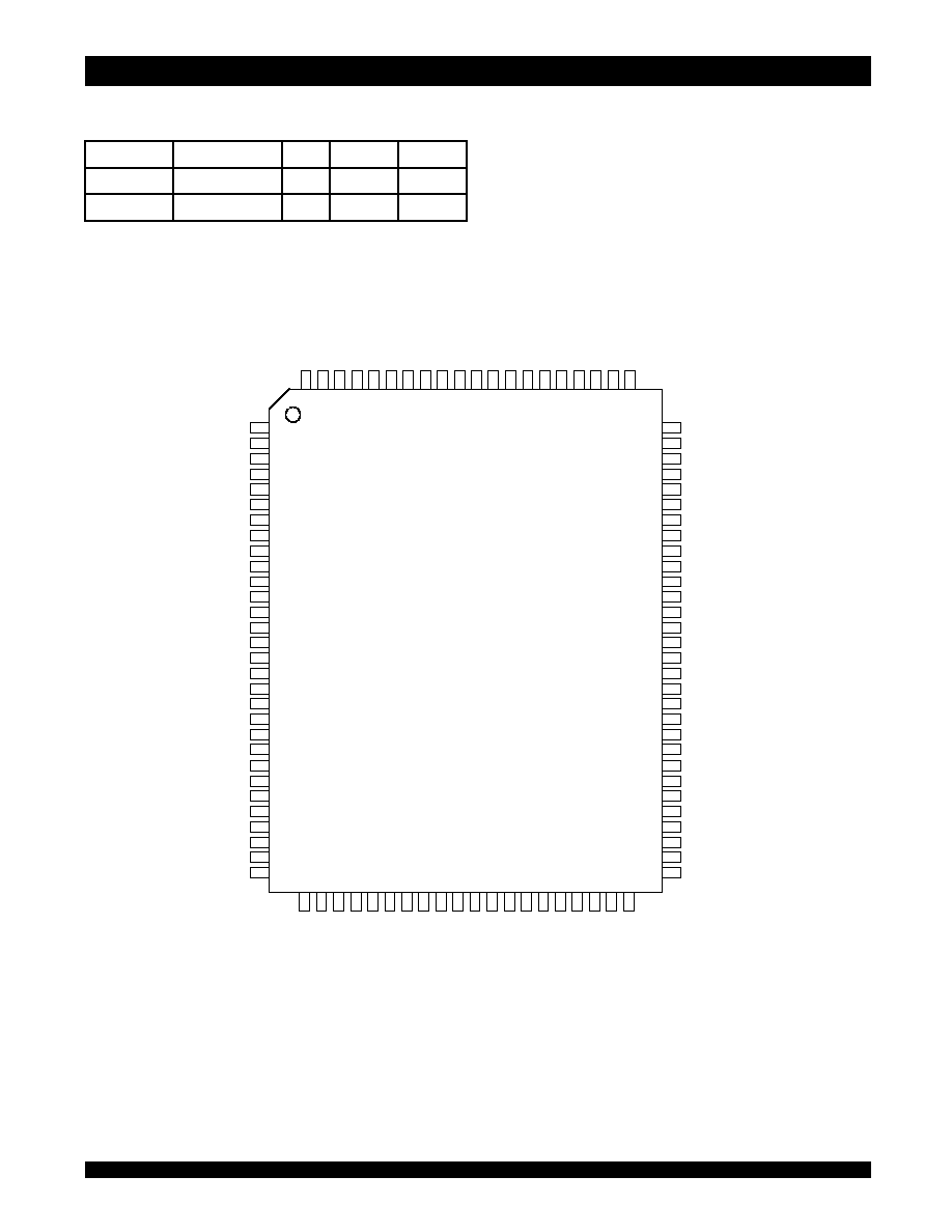
Pin Configuration - 128K x 36
NOTES:
1. Pins 14, 16 and 66 do not have to be connected directly to V
DD
as long as the input voltage is
V
IH
.
2. Pins 83 and 84 are reserved for future 8M and 16M respectively.
3. Pin 64 does not have to be connected directly to V
SS
as long as the input voltage is
V
IL
; on the latest die revision this
pin supports ZZ (sleep mode).
Top View
100 TQFP
100 99 98 97 96 95 94 93 92 91 90
87 86 85 84 83 82 81
89 88
1
2
3
4
5
6
7
8
9
10
11
12
13
14
15
16
17
18
19
20
21
22
23
24
25
26
27
28
29
30
A
6
A
7
C
E
1
C
E
2
B
W
4
B
W
3
B
W
2
B
W
1
C
E
2
V
D
D
V
S
S
C
LK
R
/
W
C
E
N
O
E
A
D
V
/
L
D
N
C
(2)
N
C
(2)
A
8
A
9
31 32 33 34 35 36 37 38 39 40 41 42 43 44 45 46 47 48 49 50
LB
O
A
14
A
13
A
12
A
11
A
10
V
D
D
V
S
S
A
0
A
1
A
2
A
3
A
4
A
5
I/O
31
I/O
30
V
DDQ
V
SS
I/O
29
I/O
28
I/O
27
I/O
26
V
SS
V
DDQ
I/O
25
I/O
24
V
SS
V
DD
I/O
23
I/O
22
V
DDQ
V
SS
I/O
21
I/O
20
I/O
19
I/O
18
V
SS
V
DDQ
I/O
17
I/O
16
80
79
78
77
76
75
74
73
72
71
70
69
68
67
66
65
64
63
62
61
60
59
58
57
56
55
54
53
52
51
I/O
14
V
DDQ
V
SS
I/O
13
I/O
12
I/O
11
I/O
10
V
SS
V
DDQ
I/O
9
I/O
8
V
SS
V
DD
I/O
7
I/O
6
V
DDQ
V
SS
I/O
5
I/O
4
I/O
3
I/O
2
V
SS
V
DDQ
I/O
1
I/O
0
5281 drw 02
V
DD
(1)
I/O
15
I/O
P3
V
DD
(1)
I/O
P4
A
15
A
16
I/O
P1
V
DD
(1)
I/O
P2
V
SS
/ZZ
(3)
,
N
C
N
C
N
C
N
C
Grade
Temperature
(1)
V
SS
V
DD
V
DDQ
Commercial
0∞C to +70∞C
0V
3.3V± 5%
3.3V± 5%
Industrial
-40∞C to +85∞C
0V
3.3V± 5%
3.3V± 5%
5281 tbl 05
NOTES:
1. T
A
is the "instant on" case temperature.