1
©1999 Integrated Device Technology, Inc.
DECEMBER 1999
DSC-3821/03
ZBT and Zero Bus Turnaround are trademarks of Integrated Device Technology, Inc. and the architecture is supported by Micron Technology and Motorola Inc.
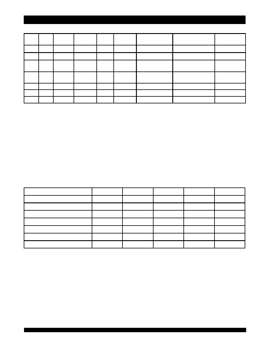
Pin Description Summary
Description
The IDT71V546 is a 3.3V high-speed 4,718,592-bit (4.5 Megabit)
synchronous SRAM organized as 128K x 36 bits. It is designed to
eliminate dead bus cycles when turning the bus around between reads
and writes, or writes and reads. Thus it has been given the name ZBT
TM
,
or Zero Bus Turn-around.
Address and control signals are applied to the SRAM during one
Features
x
x
x
x
x
128K x 36 memory configuration, pipelined outputs
x
x
x
x
x
Supports high performance system speed - 133 MHz
(4.2 ns Clock-to-Data Access)
x
x
x
x
x
ZBT
TM
Feature - No dead cycles between write and read
cycles
x
x
x
x
x
Internally synchronized registered outputs eliminate the
need to control
OE
x
x
x
x
x
Single R/
W (READ/WRITE) control pin
x
x
x
x
x
Positive clock-edge triggered address, data, and control
signal registers for fully pipelined applications
x
x
x
x
x
4-word burst capability (interleaved or linear)
x
x
x
x
x
Individual byte write (
BW
1
-
BW
4
) control (May tie active)
x
x
x
x
x
Three chip enables for simple depth expansion
x
x
x
x
x
Single 3.3V power supply (±5%)
x
x
x
x
x
Packaged in a JEDEC standard 100-pin TQFP package
clock cycle, and two cycles later its associated data cycle occurs, be it
read or write.
The IDT71V546 contains data I/O, address and control signal regis-
ters. Output enable is the only asynchronous signal and can be used to
disable the outputs at any given time.
A Clock Enable (
CEN) pin allows operation of the IDT71V546 to be
suspended as long as necessary. All synchronous inputs are ignored
when
CEN is high and the internal device registers will hold their previous
values.
There are three chip enable pins (
CE
1
, CE
2
,
CE
2
) that allow the user
to deselect the device when desired. If any one of these three is not active
when ADV/
LD is low, no new memory operation can be initiated and any
burst that was in progress is stopped. However, any pending data
transfers (reads or writes) will be completed. The data bus will tri-state two
cycles after the chip is deselected or a write initiated.
The IDT71V546 has an on-chip burst counter. In the burst mode, the
IDT71V546 can provide four cycles of data for a single address presented
to the SRAM. The order of the burst sequence is defined by the
LBO input
pin. The
LBO pin selects between linear and interleaved burst sequence.
The ADV/
LD signal is used to load a new external address (ADV/LD =
LOW) or increment the internal burst counter (ADV/
LD = HIGH).
The IDT71V546 SRAM utilizes IDT's high-performance, high-volume
3.3V CMOS process, and is packaged in a JEDEC Standard 14mm x
20mm 100-pin thin plastic quad flatpack (TQFP) for high board density.
IDT71V546
128K x 36, 3.3V Synchronous
SRAM with ZBT
TM
TM
TM
TM
TM
Feature,
Burst Counter and Pipelined Outputs
A
0
- A
16
Address Inputs
Input
Synchronous
CE
1
, CE
2
,
CE
2
Three Chip Enables
Input
Synchronous
OE
Output Enable
Input
Asynchronous
R/
W
Read/Write Signal
Input
Synchronous
CEN
Clock Enable
Input
Synchronous
BW
1
,
BW
2
,
BW
3
,
BW
4
Individual Byte Write Selects
Input
Synchronous
CLK
Clock
Input
N/A
ADV/
LD
Advance Burst Address / Load New Address
Input
Synchronous
LBO
Linear / Interleaved Burst Order
Input
Static
I/O
0
- I/O
31
, I/O
P1
- I/O
P4
Data Input/Output
I/O
Synchronous
V
DD
3.3V Power
Supply
Static
V
SS
Ground
Supply
Static
3821 tbl 01
2
IDT71V546, 128K x 36, 3.3V Synchronous SRAM with
ZBT
TM
TM
TM
TM
TM
Feature, Burst Counter and Pipelined Outputs Commercial and Industrial Temperature Ranges
Pin Definitions
(1)
NOTE:
1. All synchronous inputs must meet specified setup and hold times with respect to CLK.
Symbol
Pin Function
I/O
Active
Description
A
0
- A
16
Address Inputs
I
N/A
Synchronous Address inputs. The address register is triggered by a
combination of the rising edge of CLK and ADV/
LD Low, CEN Low and true
chip enables.
ADV/
LD
Address/Load
I
N/A
ADV/
LD is a synchronous input that is used to load the internal registers with
new address and control when it is sampled low at the rising edge of clock with
the chip selected. When ADV/
LD is low with the chip deselected, any burst in
progress is terminated. When ADV/
LD is sampled high then the internal burst
counter is advanced for any burst that was in progress. The external addresses
are ignored when ADV/
LD is sampled high.
R/
W
Read/Write
I
N/A
R/
W signal is a synchronous input that identified whether the current load cycle
initiated is a Read or Write access to the memory array. The data bus activity for
the current cycle takes place two clock cycles later.
CEN
Clock Enable
I
LOW
Synchrono us Clock Enable Input. When
CEN is sampled high, all other
synchronous inputs, includ ing clock are ignored and outputs remain unchanged.
The effect of
CEN sampled high on the device outputs is as if the low to high
clock transition did not occur. For normal operation,
CEN must be sampled low
at rising edge of clock.
BW
1
-
BW
4
Individual Byte
Write Enables
I
LOW
Synchronous byte write enables. Enable 9-bit byte has its own active low byte
write enable. On load write cycles (When R/
W and ADV/LD are sampled low)
the appropriate byte write signal (
BW
1
-
BW
4
) must be valid. The byte write
signal must also be valid on each cycle of a burst write. Byte Write signals are
ignored when R/
W is sampled high. The appropriate byte(s) of data are written
into the device two cycles later.
BW
1
-
BW
4
can all be tied low if always doing
write to the entire 36-bit word.
CE
1
,
CE
2
Chip Enables
I
LOW
Synchro nous active low chip enable.
CE
1
and
CE
2
are used with CE
2
to
enable the IDT71V546. (
CE
1
or
CE
2
sampled high or CE
2
sampled low) and
ADV/
LD low at the rising edge of clock, initiates a deselect cycle. the ZBT
TM
has a two cycle deselect, i.e., the data bus will tri-state two clock cycles after
deselect is initiated.
CE2
Chip Enable
I
HIGH
Synchronout active high chip enable. CE
2
is used with
CE
1
and
CE
2
to enable
the chip. CE
2
has inverted polarity but otherwise identical to
CE
1
and
CE
2
.
CLK
Clock
I
N/A
This is the clock input to the IDT71V546. Except for
OE, all timing references for
the device are made with respect to the rising edge of CLK.
I/O
0
- I/O
31
I/O
P1 -
I/O
P4
Data Input/Output
I/O
N/A
Synchronous data input/output (I/O) pins. Both the data input path and data
output path are registered and triggered by the rising edge of CLK.
LBO
Linear Burst
Order
I
LOW
Burst order selection input. When
LBO is high the Interleaved burst sequence is
selected. When
LBO is low the Linear burst sequence is selected. LBO is a
static DC input.
OE
Output Enable
I
LOW
Asynchronous output enable.
OE must be low to read data from the 71V546.
When
OE is high the I/O pins are in a high-impedance state. OE does not need
to be actively controlled for read and write cycles. In normal operation,
OE can
be tied low.
V
DD
Power Supply
N/A
N/A
3.3V power supply input.
V
SS
Ground
N/A
N/A
Ground pin.
3821 tbl 02
6.42
3
IDT71V546, 128K x 36, 3.3V Synchronous SRAM with
ZBT
TM
TM
TM
TM
TM
Feature, Burst Counter and Pipelined Outputs Commercial and Industrial Temperature Ranges
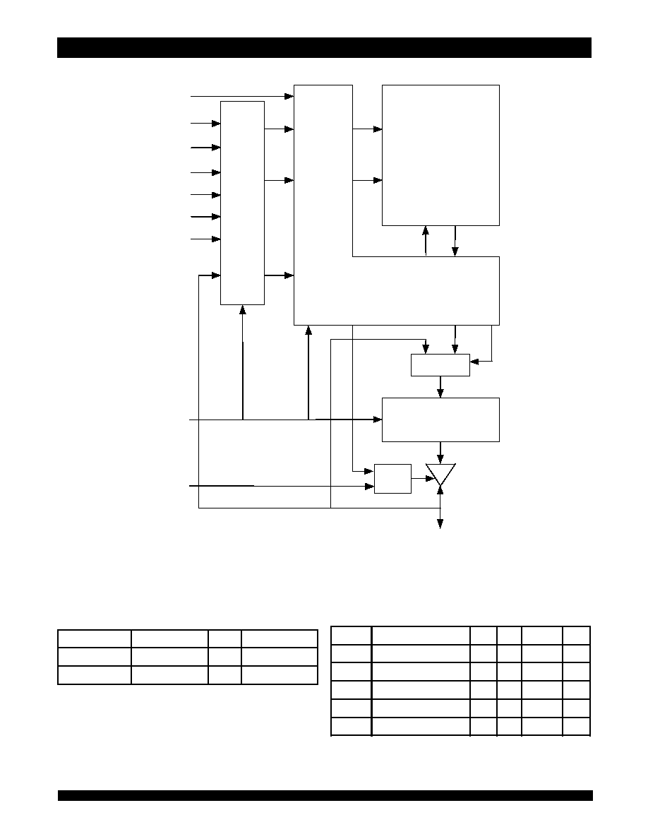
Functional Block Diagram
Recommended Operating
Temperature and Supply Voltage
Recommended DC Operating
Conditions
Clk
D
Q
D
Q
D
Q
Address A [0:16]
Control Logic
Address
Control
DI
DO
I
npu
t
R
eg
i
s
t
e
r
3821 drw 01
Clock
Data I/O [0:31], I/O P[1:4]
D
Q
Cl
k
Output Register
Mux
Sel
Gate
OE
CE
1
, CE
2
,
CE
2
R/
W
CEN
ADV/
LD
BW
x
LBO
128K x 36 BIT
MEMORY ARRAY
.
Grade
Temperature
V
SS
V
DD
Commercial
0
O
C to +70
O
C
0V
3.3V±5%
Industrial
-40
O
C to +85
O
C
0V
3.3V±5%
3821 tbl 03
NOTES:
1. V
IL
(min.) = ≠1.0V for pulse width less than t
CYC/2
, once per cycle.
2. V
IH
(max.) = +6.0V for pulse width less than t
CYC/2
, once per cycle.
Symbol
Parameter
Min.
Typ.
Max.
Unit
V
DD
Supply Voltage
3.135
3.3
3.465
V
V
SS
Ground
0
0
0
V
V
IH
Input High Voltage - Inputs
2.0
____
4.6
V
V
IH
Input High Voltage - I/O
2.0
____
V
DD
+0.3
(2)
V
V
IL
Input Low Voltage
-0.5
(1)
____
0.8
V
3821 tbl 04
4
IDT71V546, 128K x 36, 3.3V Synchronous SRAM with
ZBT
TM
TM
TM
TM
TM
Feature, Burst Counter and Pipelined Outputs Commercial and Industrial Temperature Ranges
Absolute Maximum Ratings
(1)
Capacitance
(T
A
= +25∞C, f = 1.0MHz, TQFP package)
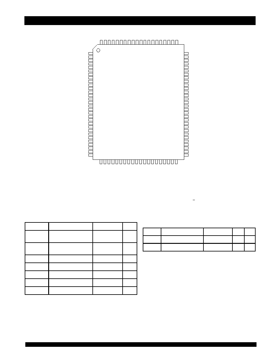
Pin Configuration
Top View
TQFP
100 99 98 97 96 95 94 93 92 91 90
87 86 85 84 83 82 81
89 88
1
2
3
4
5
6
7
8
9
10
11
12
13
14
15
16
17
18
19
20
21
22
23
24
25
26
27
28
29
30
A
6
A
7
C
E
1
C
E
2
B
W
4
B
W
3
B
W
2
B
W
1
C
E
2
V
D
D
V
S
S
C
LK
R
/
W
C
E
N
O
E
A
D
V
/
LD
N
C
(2
)
N
C
(2
)
A
8
A
9
31 32 33 34 35 36 37 38 39 40 41 42 43 44 45 46 47 48 49 50
N
C
N
C
N
C
N
C
LB
O
A
14
A
13
A
12
A
11
A
10
V
D
D
V
S
S
A
0
A
1
A
2
A
3
A
4
A
5
I/O
31
I/O
30
V
DD
V
SS
I/O
29
I/O
28
I/O
27
I/O
26
V
SS
V
DD
I/O
25
I/O
24
V
SS
V
DD
I/O
23
I/O
22
V
DD
V
SS
I/O
21
I/O
20
I/O
19
I/O
18
V
SS
V
DD
I/O
17
I/O
16
80
79
78
77
76
75
74
73
72
71
70
69
68
67
66
65
64
63
62
61
60
59
58
57
56
55
54
53
52
51
I/O
14
V
DD
V
SS
I/O
13
I/O
12
I/O
11
I/O
10
V
SS
V
DD
I/O
9
I/O
8
V
SS
V
DD
I/O
7
I/O
6
V
DD
V
SS
I/O
5
I/O
4
I/O
3
I/O
2
V
SS
V
DD
I/O
1
I/O
0
PK100-1
3821 drw 02
V
DD
(1)
I/O
15
I/O
P3
V
DD
I/O
P4
A
15
A
16
I/O
P1
V
DD
I/O
P2
V
SS
.
.
Symbol
Rating
Value
Unit
V
TERM
(2)
Terminal Voltage
with Respect to GND
-0.5 to +4.6
V
V
TERM
(3)
Terminal Voltage
with Respect to GND
-0.5 to V
DD
+0.5
V
T
A
Operating Temperature
0 to +70
o
C
T
BIAS
Temperature Under Bias
-55 to +125
o
C
T
STG
Storage Temperature
-55 to +125
o
C
P
T
Power Dissipation
2.0
W
I
OUT
DC Output Current
50
mA
3821 tbl 05
NOTES:
1. Stresses greater than those listed under ABSOLUTE MAXIMUM RATINGS
may cause permanent damage to the device. This is a stress rating only
and functional operation of the device at these or any other conditions above
those indicated in the operational sections of this specification is not implied.
Exposure to absolute maximum rating conditions for extended periods may
affect reliability.
2. V
DD
and Input terminals only.
3. I/O terminals.
NOTE:
1. This parameter is guaranteed by device characterization, but not production
tested.
Symbol
Parameter
(1)
Conditions
Max.
Unit
C
IN
Input Capacitance
V
IN
= 3dV
5
pF
C
I/O
I/O Capacitance
V
OUT
= 3dV
7
pF
3821 tbl 06
NOTES:
1. Pin 14 does not have to be connected directly to V
DD
as long as the input voltage is > V
IH
.
2. Pins 83 and 84 are reserved for future A
17
(8M) and A
18
(16M) respectively.
6.42
5
IDT71V546, 128K x 36, 3.3V Synchronous SRAM with
ZBT
TM
TM
TM
TM
TM
Feature, Burst Counter and Pipelined Outputs Commercial and Industrial Temperature Ranges
Synchronous Truth Table
(1)
Partial Truth Table for Writes
(1)
NOTES:
1. L = V
IL
, H = V
IH
, X = Don't Care.
2. When ADV/
LD signal is sampled high, the internal burst counter is incremented. The R/W signal is ignored when the counter is advanced. Therefore the nature of
the burst cycle (Read or Write) is determined by the status of the R/
W signal when the first address is loaded at the beginning of the burst cycle.
3. Deselect cycle is initiated when either (
CE
1
, or
CE
2
is sampled high or CE
2
is sampled low) and ADV/
LD is sampled low at rising edge of clock. The data bus will
tri-state two cycles after deselect is initiated.
4. When
CEN is sampled high at the rising edge of clock, that clock edge is blocked from propogating through the part. The state of all the internal registers and the I/
Os remains unchanged.
5. To select the chip requires
CE
1
= L,
CE
2
= L, CE
2
= H on these chip enables. Chip is deselected if either one of the chip enables is false.
6. Device Outputs are ensured to be in High-Z after the first rising edge of clock upon power-up.
7. Q - Data read from the device, D - data written to the device.
CEN
R/
W
Chip
(5)
Enable
ADV/
LD
BWx
ADDRESS
USED
PREVIOUIS CYCLE
CURRENT CYCLE
I/O
(2 cycles later)
L
L
Select
L
Valid
External
X
LOAD WRITE
D
(7)
L
H
Select
L
X
External
X
LOAD READ
Q
(7)
L
X
X
H
Valid
Internal
LOAD WRITE/
BURST WRITE
BURST WRITE
(Advance Burst Counter)
(2)
D
(7)
L
X
X
H
X
Internal
LOAD READ/
BURST READ
BURST READ
(Advance Burst Counter)
(2)
Q
(7)
L
X
Deselect
L
X
X
X
DESELECT or STOP
(3)
HiZ
L
X
X
H
X
X
DESELECT / NOOP
NOOP
HiZ
H
X
X
X
X
X
X
SUSPEND
(4)
Previous Value
3821 tbl 07
NOTES:
1. L = V
IL
, H = V
IH
, X = Don't Care.
2. Multiple bytes may be selected during the same cycle.
Operation
R/
W
BW
1
BW
2
BW
3
BW
4
READ
H
X
X
X
X
WRITE ALL BYTES
L
L
L
L
L
WRITE BYTE 1 (I/O [0:7], I/O
P1
)
(2)
L
L
H
H
H
WRITE BYTE 2 (I/O [8:15], I/O
P2
)
(2)
L
H
L
H
H
WRITE BYTE 3 (I/O [16:23], I/O
P3
)
(2)
L
H
H
L
H
WRITE BYTE 4 (I/O [24:31], I/O
P4
)
(2)
L
H
H
H
L
NO WRITE
L
H
H
H
H
3821 tbl 08