AUGUST 2001
DSC-3619/04
1
©2000 Integrated Device Technology, Inc.
Features
x
x
x
x
x
64K x 32 memory configuration
x
x
x
x
x
Supports high system speed:
Commercial:
≠ A4 4.5ns clock access time (117 MHz)
Commercial and Industrial:
≠ 5
5ns clock access time (100 MHz)
≠ 6
6ns clock access time (83 MHz)
≠ 7
7ns clock access time (66 MHz)
x
x
x
x
x
Single-cycle deselect functionality (Compatible with
Micron Part # MT58LC64K32D7LG-XX)
x
x
x
x
x
LBO input selects interleaved or linear burst mode
x
x
x
x
x
Self-timed write cycle with global write control (
GW), byte
write enable (
BWE), and byte writes (BWx)
x
x
x
x
x
Power down controlled by ZZ input
x
x
x
x
x
Operates with a single 3.3V power supply (+10/-5%)
x
x
x
x
x
Packaged in a JEDEC Standard 100-pin rectangular plastic
thin quad flatpack (TQFP).
Description
The IDT71V632 is a 3.3V high-speed SRAM organized as 64K x 32
Pin Description Summary
Pentium processor is a trademark of Intel Corp.
PowerPC is a trademark of International Business Machines, Inc.
64K x 32
3.3V Synchronous SRAM
Pipelined Outputs
Burst Counter, Single Cycle Deselect
IDT71V632
with full support of the PentiumTM and PowerPCTM processor interfaces.
The pipelined burst architecture provides cost-effective 3-1-1-1 second-
ary cache performance for processors up to 117MHz.
The IDT71V632 SRAM contains write, data, address, and control
registers. Internal logic allows the SRAM to generate a self-timed write
based upon a decision which can be left until the extreme end of the write
cycle.
The burst mode feature offers the highest level of performance to the
system designer, as the IDT71V632 can provide four cycles of data for
a single address presented to the SRAM. An internal burst address counter
accepts the first cycle address from the processor, initiating the access
sequence. The first cycle of output data will be pipelined for one cycle before
it is available on the next rising clock edge. If burst mode operation is
selected (
ADV=LOW), the subsequent three cycles of output data will be
available to the user on the next three rising clock edges. The order of these
three addresses will be defined by the internal burst counter and the
LBO
input pin.
The IDT71V632 SRAM utilizes IDT's high-performance, high-volume
3.3V CMOS process, and is packaged in a JEDEC Standard 14mm x
20mm 100-pin thin plastic quad flatpack (TQFP) for optimum board density
in both desktop and notebook applications.
A
0
≠A
15
Address Inputs
Input
Synchronous
CE
Chip Enable
Input
Synchronous
CS
0
,
CS
1
Chips Selects
Input
Synchronous
OE
Output Enable
Input
Asynchronous
GW
Global Write Enable
Input
Synchronous
BWE
Byte Write Enable
Input
Synchronous
BW
1,
BW
2,
BW
3,
BW
4
Individual Byte Write Selects
Input
Synchronous
CLK
Clock
Input
N/A
ADV
Burst Address Advance
Input
Synchronous
ADSC
Address Status (Cache Controller)
Input
Synchronous
ADSP
Address Status (Processor)
Input
Synchronous
LBO
Linear / Interleaved Burst Order
Input
DC
ZZ
Sleep Mode
Input
Asynchronous
I/O
0
≠I/O
31
Data Input/Output
I/O
Synchronous
V
DD
, V
DDQ
3.3V
Power
N/A
V
SS
, V
SSQ
Array Ground, I/O Ground
Power
N/A
3619 tbl 01

6.42
2
IDT71V632, 64K x 32, 3.3V Synchronous SRAM
with Pipelined Outputs and Single Cycle Deselect Commercial and Industrial Temperature Ranges
Symbol
Pin Function
I/O
Active
Description
A
0
≠A
15
Address Inputs
I
N/A
Synchronous Address inputs. The address re gister is triggered by a combination
of the rising edge of CLK and
ADSC Low or ADSP Low and CE Low.
ADSC
Address Status
(Cache Controller)
I
LOW
Synchronous Address Status from Cache Controller.
ADSC is an active LOW
input that is used to load the add ress registers with new addresses.
ADSC is
NOT GATED by
CE.
ADSP
Address Status
(Processor)
I
LOW
Synchrono us Address Status from Processor.
ADSP is an active LOW input that
is used to load the address registers with new addresses.
ADSP is gated by
CE.
ADV
Burst Address Advance
I
LOW
Synchronous Address Advance.
ADV is an active LOW input that is used to
advance the internal burst counter, co ntrolling burst access after the initial
address is loaded. When this input is HIGH the burst counter is not incremented;
that is, there is no address advance.
BWE
Byte Write Enable
I
LOW
Synchronous byte write enable gates the byte write inputs
BW
1
≠
BW
4
. If
BWE is
LOW at the rising edge of CLK then
BW
X
inputs are passed to the next stage in
the circuit. A byte write can still be blocked if
ADSP is LOW at the rising edge of
CLK. If
ADSP is HIGH and BW
X
is LOW at the rising edge of CLK then data will
be written to the SRAM. If
BWE is HIGH then the byte write inputs are blocked
and only
GW can initiate a write cycle.
BW
1
≠
BW
4
Individual Byte
Write Enables
I
LOW
Synchronous byte write enables.
BW
1
controls I/O(7:0),
BW
2
controls I/O(15:8),
etc. Any active byte write causes all outputs to be disabled.
ADSP LOW
disables all byte writes.
BW
1
≠
BW
4
must meet specified setup and hold times
with respect to CLK.
CE
Chip Enable
I
LOW
Synchronous chip enable.
CE is used with CS
0
and
CS
1
to enable the
IDT71V632.
CE also gates ADSP.
CLK
Clock
I
N/A
This is the clock input. All timing references for the device are made with respect
to this input.
CS
0
Chip Select 0
I
HIGH
Synchronous active HIGH chip select. CS
0
is used with
CE and CS
1
to enable
the chip.
CS
1
Chip Select 1
I
LOW
Synchronous active LOW chip select.
CS
1
is used with
CE and CS
0
to enable
the chip.
GW
Global Write Enable
I
LOW
Synchrono us global write enable. This input will write all four 8-bit data bytes
when LOW on the rising edge of CLK.
GW supercedes individual byte write
enables.
I/O
0
≠I/O
31
Data Input/Output
I/O
N/A
Synchronous data input/output (I/O) pins. Both the data input path and data output
path are registered and triggered by the rising edge of CLK.
LBO
Linear Burst Order
I
LOW
Asynchronous burst order sele ction DC input. When
LBO is HIGH the Interleaved
(Intel) burst sequence is selected. When
LBO is LOW the Linear (PowerPC) burst
sequence is selected.
LBO is a static DC input and must not change state while
the device is operating.
OE
Output Enable
I
LOW
Asynchronous output enable. When
OE is LOW the data output drivers are
enabled on the I/O pins if the chip is also selected. When
OE is HIGH the I/O
pins are in a high-impedence state.
V
DD
Power Supply
N/A
N/A
3.3V core power supply inputs.
V
DDQ
Power Supply
N/A
N/A
3.3V I/O power supply inputs.
V
SS
Ground
N/A
N/A
Core ground pins.
V
SSQ
Ground
N/A
N/A
I/O ground pins.
NC
No Connect
N/A
N/A
NC pins are not electrically connected to the chip.
ZZ
Sleep Mode
I
HIGH
Asynchronous sleep mode input. ZZ HIGH will gate the CLK internally and power
down the IDT71V632 to its lowest power consumption level. Data retention is
guaranteed in Sleep Mode.
3619 tbl 02
Pin Definitions
(1)
NOTE:
1. All synchronous inputs must meet specified setup and hold times with respect to CLK.
6.42
3
IDT71V632, 64K x 32, 3.3V Synchronous SRAM
with Pipelined Outputs and Single Cycle Deselect Commercial and Industrial Temperature Ranges
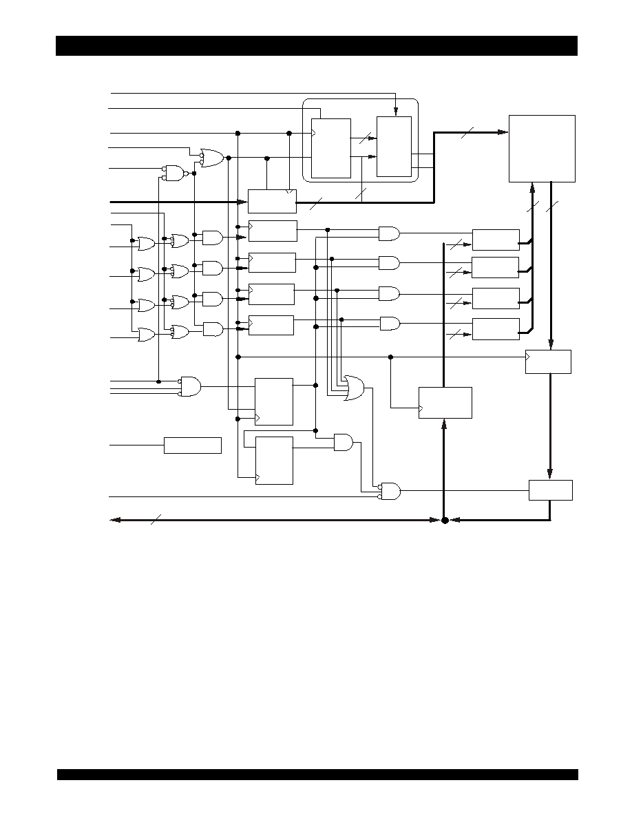
Functional Block Diagram
A
0
≠A
15
ADDRESS
REGISTER
CLR
A
1
*
A
0
*
16
2
16
A
2
≠A
15
64K x 32
BIT
MEMORY
ARRAY
INTERNAL
ADDRESS
A
0
, A
1
BW
4
BW
3
BW
2
BW
1
Byte 1
Write Register
32
32
ADSP
ADV
CLK
ADSC
CS0
CS
1
Byte 1
Write Driver
Byte 2
Write Driver
Byte 3
Write Driver
Byte 4
Write Driver
Byte 2
Write Register
Byte 3
Write Register
Byte 4
Write Register
8
8
8
8
GW
CE
BWE
LBO
I/O
0
≠I/O
31
OE
DATA INPUT
REGISTER
32
OUTPUT
BUFFER
OUTPUT
REGISTER
Powerdown
ZZ
D
Q
D
Q
Enable
Register
Enable
Delay
Register
OE
Burst
Sequence
CE
CLK EN
CLK EN
Q1
Q0
2
Burst
Logic
Binary
Counter
3619 drw 01
.
6.42
4
IDT71V632, 64K x 32, 3.3V Synchronous SRAM
with Pipelined Outputs and Single Cycle Deselect Commercial and Industrial Temperature Ranges
Symbol
Parameter
(1)
Conditions
Max.
Unit
C
IN
Input Capacitance
V
IN
= 3dV
6
pF
C
I/O
I/O Capacitance
V
OUT
= 3dV
7
pF
3619 tbl 06
Absolute Maximum Ratings
(1)
Capacitance
(T
A
= +25∞C, f = 1.0MHz, TQFP package)
NOTES:
1. Stresses greater than those listed under ABSOLUTE MAXIMUM RATINGS may
cause permanent damage to the device. This is a stress rating only and functional
operation of the device at these or any other conditions above those indicated
in the operational sections of this specification is not implied. Exposure to absolute
maximum rating conditions for extended periods may affect reliability.
2. V
DD
, V
DDQ
and Input terminals only.
3. I/O terminals.
NOTE:
1. This parameter is guaranteed by device characterization, but not production
tested.
Symbol
Rating
Value
Unit
V
TERM
(2)
Terminal Voltage with
Respect to GND
≠0.5 to +4.6
V
V
TERM
(3)
Terminal Voltage with
Respect to GND
≠0.5 to V
DD
+0.5
V
T
A
Operating Temperature
0 to +70
o
C
T
BIAS
Temperature Under Bias
≠55 to +125
o
C
T
STG
Storage Temperature
≠55 to +125
o
C
P
T
Power Dissipation
1.0
W
I
OUT
DC Output Current
50
mA
3619 tbl 05
Recommended DC Operating
Conditions
NOTES:
1. V
IH
(max) = 6.0V for pulse width less than t
CYC
/2, once per cycle.
2. V
IH
(max) = V
DDQ
+ 1.0V for pulse width less than t
CYC
/2, once per cycle.
3. V
IL
(min) = ≠1.0V for pulse width less than t
CYC
/2, once per cycle.
S ym bol
P aram eter
M in.
M ax.
Unit
V
DD
Co re S up p ly Vo ltag e
3.135
3.63
V
V
DDQ
I/O S up p ly Vo ltag e
3.135
3.63
V
V
SS,
V
SSQ
G ro und
0
0
V
V
IH
Inp ut Hig h Vo ltag e -- Inp uts
2.0
5.0
(1)
V
V
IH
Inp ut Hig h Vo ltag e -- I/O
2.0
V
DDQ
+ 0.3
(2)
V
V
IL
Inp ut Lo w Vo ltag e
≠0.3
(3)
0.8
V
3619 tbl 04
Recommended Operating
Temperature and Supply Voltage
Grade
Temperature
V
SS
V
DD
V
DDQ
Commercial
0∞C to +70∞C
0V
3.3V+10/-5% 3.3V+10/-5%
Industrial
≠40∞C to +85∞C
0V
3.3V+10/-5% 3.3V+10/-5%
3619 tbl 03
6.42
5
IDT71V632, 64K x 32, 3.3V Synchronous SRAM
with Pipelined Outputs and Single Cycle Deselect Commercial and Industrial Temperature Ranges
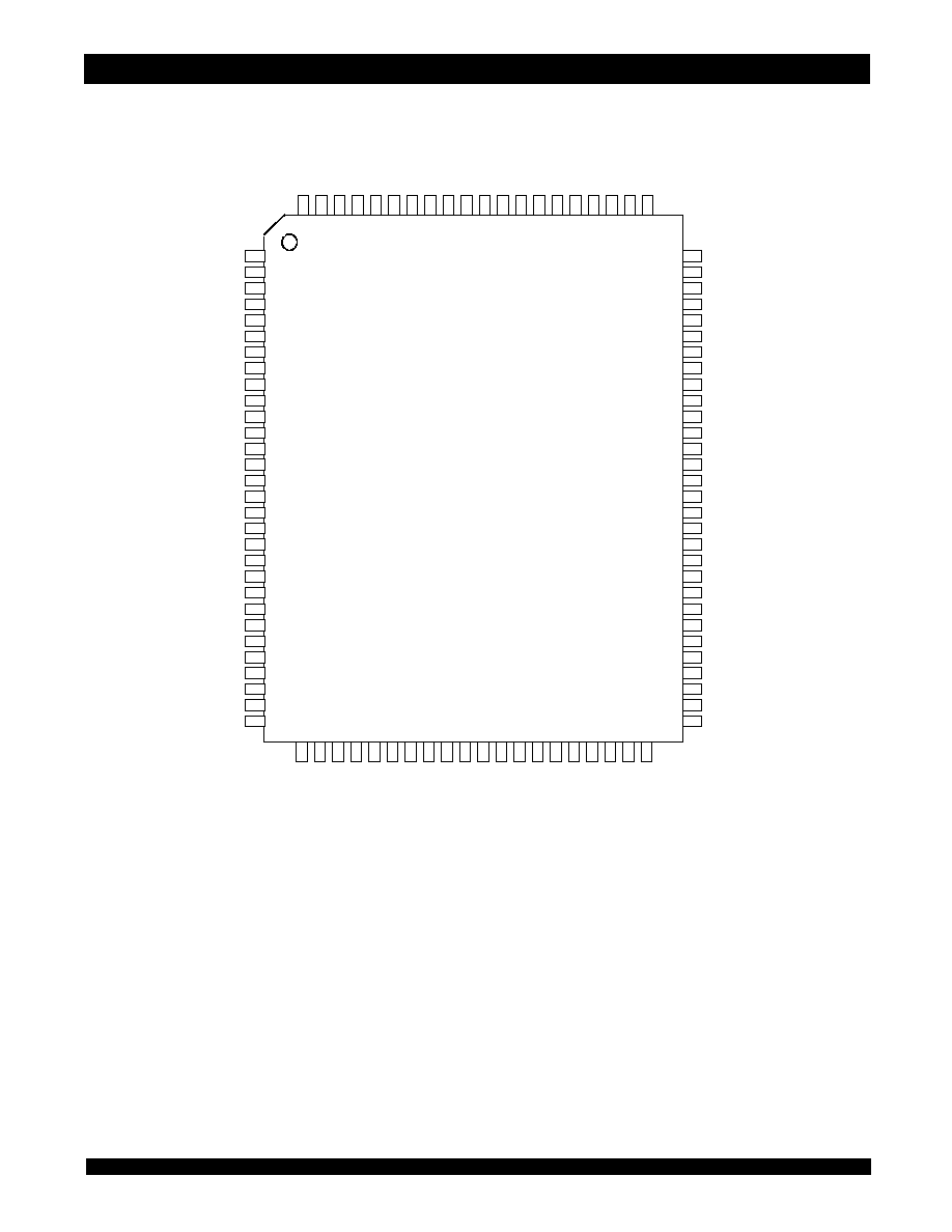
Pin Configuration
Top View TQFP
100 99 98 97 96 95 94 93 92 91 90
87 86 85 84 83 82 81
89 88
1
2
3
4
5
6
7
8
9
10
11
12
13
14
15
16
17
18
19
20
21
22
23
24
25
26
27
28
29
30
A
6
A
7
C
E
C
S
0
B
W
4
B
W
3
B
W
2
B
W
1
C
S
1
V
D
D
V
S
S
C
LK
G
W
B
W
E
O
E
A
D
S
C
A
D
S
P
A
D
V
A
8
A
9
NC
31 32 33 34 35 36 37 38 39 40 41 42 43 44 45 46 47 48 49 50
N
C
N
C
N
C
N
C
N
C
LB
O
A
14
A
13
A
12
A
11
A
10
V
D
D
V
S
S
A
0
A
1
A
2
A
3
A
4
A
5
NC
I/O
31
I/O
30
V
DDQ
V
SSQ
I/O
29
I/O
28
I/O
27
I/O
26
V
SSQ
V
DDQ
I/O
25
I/O
24
V
SS
V
DD
I/O
23
I/O
22
V
DDQ
V
SSQ
I/O
21
I/O
20
I/O
19
I/O
18
V
SSQ
V
DDQ
I/O
17
I/O
16
NC
80
79
78
77
76
75
74
73
72
71
70
69
68
67
66
65
64
63
62
61
60
59
58
57
56
55
54
53
52
51
NC
I/O
14
V
DDQ
V
SSQ
I/O
13
I/O
12
I/O
11
I/O
10
V
SSQ
V
DDQ
I/O
9
I/O
8
V
SS
NC
V
DD
ZZ
(2)
I/O
7
I/O
6
V
DDQ
V
SSQ
I/O
5
I/O
4
I/O
3
I/O
2
V
SSQ
V
DDQ
I/O
1
I/O
0
NC
PK100-1
3619 drw 02
V
DD
/NC
(1)
I/O
15
A
15
NOTES:
1. Pin 14 can either be directly connected to V
DD
or not connected.
2. Pin 64 can be left unconnected and the device will always remain in active mode.