 | –≠–ª–µ–∫—Ç—Ä–æ–Ω–Ω—ã–π –∫–æ–º–ø–æ–Ω–µ–Ω—Ç: 71V67802 | –°–∫–∞—á–∞—Ç—å:  PDF PDF  ZIP ZIP |
APRIL 2003
DSC-5311/06
1
©2002 Integrated Device Technology, Inc.
A
0
-A
18
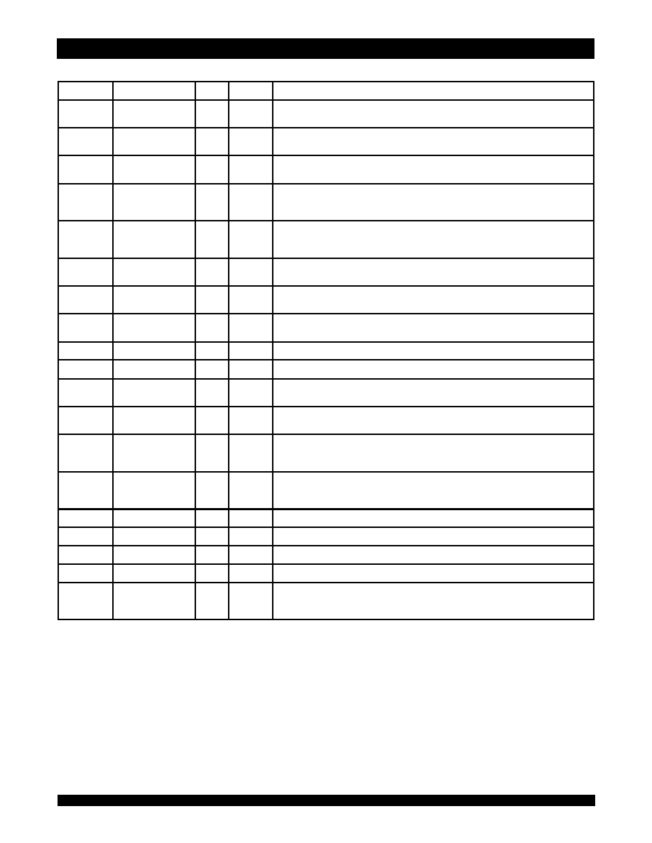
Address Inputs
Input
Synchronous
CE
Chip Enable
Input
Synchronous
CS
0
,
CS
1
Chip Selects
Input
Synchronous
OE
Output Enable
Input
Asynchronous
GW
Global Write Enable
Input
Synchronous
BWE
Byte Write Enable
Input
Synchronous
BW
1
,
BW
2
,
BW
3
,
BW
4
(1)
Individual Byte Write Selects
Input
Synchronous
CLK
Clock
Input
N/A
ADV
Burst Address Advance
Input
Synchronous
ADSC
Address Status (Cache Controller)
Input
Synchronous
ADSP
Address Status (Processor)
Input
Synchronous
LBO
Linear / Interleaved Burst Order
Input
DC
ZZ
Sleep Mode
Input
Asynchronous
I/O
0
-I/O
31
, I/O
P1
-I/O
P4
Data Input / Output
I/O
Synchronous
V
DD
, V
DDQ
Core Power, I/O Power
Supply
N/A
V
SS
Ground
Supply
N/A
5311 tbl 01
Features
x
x
x
x
x
256K x 36, 512K x 18 memory configurations
x
x
x
x
x
Supports high system speed:
≠ 166MHz 3.5ns clock access time
≠ 150MHz 3.8ns clock access time
≠ 133MHz 4.2ns clock access time
x
x
x
x
x
LBO input selects interleaved or linear burst mode
x
x
x
x
x
Self-timed write cycle with global write control (
GW), byte
write enable (
BWE), and byte writes (BWx)
x
x
x
x
x
3.3V core power supply
x
x
x
x
x
Power down controlled by ZZ input
x
x
x
x
x
2.5V I/O supply (V
DDQ
)
x
x
x
x
x
Packaged in a JEDEC Standard 100-pin plastic thin quad
flatpack (TQFP), 119 ball grid array (BGA) and 165 fine pitch
ball grid array.
Pin Description Summary
NOTE:
1.
BW
3
and
BW
4
are not applicable for the IDT71V67802.
256K X 36, 512K X 18
3.3V Synchronous SRAMs
2.5V I/O, Burst Counter
Pipelined Outputs, Single Cycle Deselect
IDT71V67602
IDT71V67802
Description
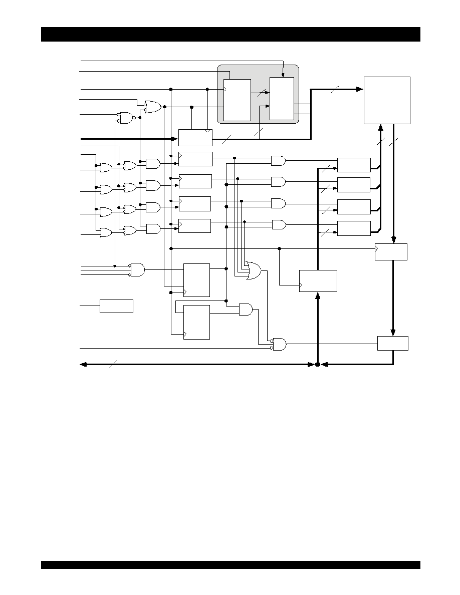
The IDT71V67602/7802 are high-speed SRAMs organized as
256K x 36/512K x 18. The IDT71V676/78 SRAMs contain write, data,
address and control registers. Internal logic allows the SRAM to generate
a self-timed write based upon a decision which can be left until the end of
the write cycle.
The burst mode feature offers the highest level of performance to the
system designer, as the IDT71V676
02
/78
02
can provide four cycles of
data for a single address presented to the SRAM. An internal burst address
counter accepts the first cycle address from the processor, initiating the
access sequence. The first cycle of output data will be pipelined for one
cycle before it is available on the next rising clock edge. If burst mode
operation is selected (
ADV=LOW), the subsequent three cycles of output
data will be available to the user on the next three rising clock edges. The
order of these three addresses are defined by the internal burst counter
and the
LBO input pin.
The IDT71V67602/7802 SRAMs utilize IDT's latest high-performance
CMOS process and are packaged in a JEDEC standard 14mm x 20mm
100-pin thin plastic quad flatpack (TQFP) as well as a 119 ball grid array
(BGA) and 165 fine pitch ball grid array (fBGA).
6.42
2
IDT71V67602, IDT71V67802, 256K x 36, 512K x 18, 3.3V Synchronous Commercial and Industrial Temperature Ranges
SRAMs with 2.5V I/O, Pipelined Outputs, Single Cycle Deselect
Symbol
Pin Function
I/O
Active
Description
A
0
-A
18
Address Inputs
I
N/A
Synchronous Address inputs. The address register is trig gered by a combination of the
rising edge of CLK and
ADSC Low or ADSP Low and CE Low.
ADSC
Address Status
(Cache Controller)
I
LOW
Synchronous Address Status from Cache Controller.
ADSC is an active LOW input that is
used to load the address registers with new addresses.
ADSP
Address Status
(Processor)
I
LOW
Synchronous Address Status from Processor.
ADSP is an active LOW input that is used to
load the address registers with new addresses.
ADSP is gated by CE.
ADV
Burst Address
Advance
I
LOW
Synchronous Address Advance.
ADV is an active LOW input that is used to advance the
internal burst counter, controlling burst access after the initial address is loaded. When the
input is HIGH the burst counter is not incremented; that is, there is no address advance.
BWE
Byte Write Enable
I
LOW
Synchronous byte write enable gates the byte write inputs
BW
1
-
BW
4
. If
BWE is LOW at the
rising edge of CLK then
BWx inputs are passed to the next stage in the circuit. If BWE is
HIGH then the byte write inputs are blocked and only
GW can initiate a write cycle.
BW
1
-
BW
4
Individual Byte
Write Enables
I
LOW
Synchronous byte write enables.
BW
1
controls I/O
0-7
, I/O
P1
,
BW
2
controls I/O
8-15
, I/O
P2
, etc.
Any active byte write causes all outputs to be disabled.
CE
Chip Enable
I
LOW
Synchronous chip enable.
CE is used with CS
0
and
CS
1
to enable the IDT71V67602/7802.
CE also gates ADSP.
CLK
Clock
I
N/A
This is the clock input. All timing references for the device are made with respect to this
input.
CS
0
Chip Select 0
I
HIGH
Synchrono us active HIGH chip select. CS
0
is used with
CE and CS
1
to enable the chip.
CS
1
Chip Select 1
I
LOW
Synchronous active LOW chip select.
CS
1
is used with
CE and CS
0
to enable the chip.
GW
Global Write
Enable
I
LOW
Synchronous global write enable. This input will write all four 9-bit data bytes when LOW
on the rising edge of CLK.
GW supersedes individual byte write enables.
I/O
0
-I/O
31
I/O
P1
-I/O
P4
Data Input/Output
I/O
N/A
Synchro nous data input/output (I/O) pins. Both the data input path and data output path are
registered and triggered by the rising edge of CLK.
LBO
Linear Burst Order
I
LOW
Asynchronous burst order selection input. When
LBO is HIGH, the interleaved burst
sequence is selected. When
LBO is LOW the Linear burst sequence is selected. LBO is a
static input and must not change state while the device is operating.
OE
Output Enable
I
LOW
Asynchronous output enable. When
OE is LOW the data output drivers are enabled on the
I/O pins if the chip is also selected. When
OE is HIGH the I/O pins are in a high-
impedance state.
V
DD
Power Supply
N/A
N/A
3.3V core power supply.
V
DDQ
Power Supply
N/A
N/A
2.5V I/O Supply.
V
SS
Ground
N/A
N/A
Ground.
NC
No Connect
N/A
N/A
NC pins are not electrically connected to the device.
ZZ
Sleep Mode
I
HIGH
Asynchro nous sleep mode input. ZZ HIGH will gate the CLK internally and power down the
IDT71V67602/7802 to its lowest p ower consumption level. Data retention is guaranteed in
Sleep Mode.
5311 tbl 02
Pin Definitions
(1)
NOTE:
1. All synchronous inputs must meet specified setup and hold times with respect to CLK.
6.42
3
IDT71V67602, IDT71V67802, 256K x 36, 512K x 18, 3.3V Synchronous Commercial and Industrial Temperature Ranges
SRAMs with 2.5V I/O, Pipelined Outputs, Single Cycle Deselect
Functional Block Diagram
A
0≠
A
17/18
ADDRESS
REGISTER
CLR
A1*
A0*
18/19
2
18/19
A
2
≠A
18
256K x 36/
512K x 18-
BIT
MEMORY
ARRAY
INTERNAL
ADDRESS
A
0
,A
1
BW
4
BW
3
BW
2
BW
1
Byte 1
Write Register
36/18
36/18
ADSP
ADV
CLK
ADSC
CS
0
CS
1
Byte 1
Write Driver
Byte 2
Write Driver
Byte 3
Write Driver
Byte 4
Write Driver
Byte 2
Write Register
Byte 3
Write Register
Byte 4
Write Register
9
9
9
9
GW
CE
BWE
LBO
I/O
0
≠I/O
31
I/O
P1
≠I/O
P4
OE
DATA INPUT
REGISTER
36/18
OUTPUT
BUFFER
OUTPUT
REGISTER
D
Q
D
Q
Enable
Register
Enable
Delay
Register
OE
Burst
Sequence
CEN
CLK EN
CLK EN
Q1
Q0
2
Burst
Logic
Binary
Counter
5311 drw 01
ZZ
Powerdown
,
6.42
4
IDT71V67602, IDT71V67802, 256K x 36, 512K x 18, 3.3V Synchronous Commercial and Industrial Temperature Ranges
SRAMs with 2.5V I/O, Pipelined Outputs, Single Cycle Deselect
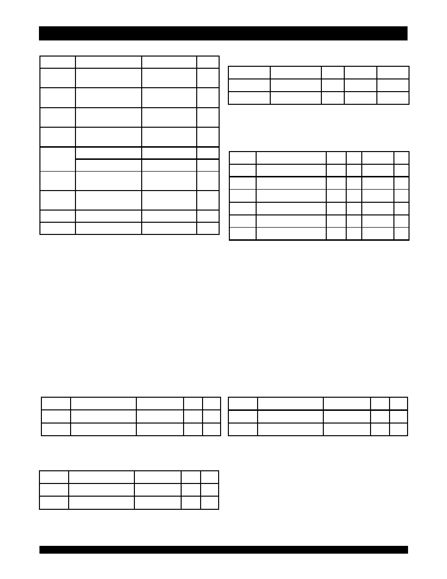
100-pin TQFP Capacitance
(T
A
= +25∞C, f = 1.0MHz)
Recommended Operating
Temperature and Supply Voltage
Absolute Maximum Ratings
(1)
NOTES:
1. Stresses greater than those listed under ABSOLUTE MAXIMUM RATINGS may
cause permanent damage to the device. This is a stress rating only and functional
operation of the device at these or any other conditions above those indicated
in the operational sections of this specification is not implied. Exposure to absolute
maximum rating conditions for extended periods may affect reliability.
2. V
DD
terminals only.
3. V
DDQ
terminals only.
4. Input terminals only.
5. I/O terminals only.
6. This is a steady-state DC parameter that applies after the power supplies have
ramped up. Power supply sequencing is not necessary; however, the voltage
on any input or I/O pin cannot exceed V
DDQ
during power supply ramp up.
7. T
A
is the "instant on" case temperature.
NOTE:
1. This parameter is guaranteed by device characterization, but not production tested.
S ym bol
Rating
Com m ercial
Unit
V
TE RM
(2)
Te rm inal Vo ltag e with
Re s p e c t to G ND
-0.5 to + 4.6
V
V
TE RM
(3,6)
Te rm inal Vo ltag e with
Re s p e c t to G ND
-0.5 to V
DD
V
V
TE RM
(4,6)
Te rm inal Vo ltag e with
Re s p e c t to G ND
-0.5 to V
DD
+ 0.5
V
V
TE RM
(5,6)
Te rm inal Vo ltag e with
Re s p e c t to G ND
-0.5 to V
DDQ
+ 0.5
V
T
A
( 7)
Co m m e rc ial
-0 to + 70
o
C
Ind us trial
-40 to + 85
o
C
T
B IA S
Te m p e rature
Und e r B ias
-55 to + 125
o
C
T
S TG
S to rag e
Te m p e rature
-55 to + 125
o
C
P
T
P o we r Dis s ip atio n
2.0
W
I
O UT
DC O utp ut Curre nt
50
m A
5311 tbl 03
Grade
Temperature
(1)
V
SS
V
DD
V
DDQ
Commercial
0∞C to +70∞C
0V
3.3V±5%
2.5V±5%
Industrial
-40∞C to +85∞C
0V
3.3V±5%
2.5V±5%
5311 tbl 04
Symbol
Parameter
(1)
Conditions
Max.
Unit
C
IN
Input Capacitance
V
IN
= 3dV
5
pF
C
I/O
I/O Capacitance
V
OUT
= 3dV
7
pF
5311 tbl 07
Symbol
Parameter
Min.
Typ.
Max.
Unit
V
DD
Core Supply Voltage
3.135
3.3
3.465
V
V
DDQ
I/O Supply Voltage
2.375
2.5
2.625
V
V
SS
Ground
0
0
0
V
V
IH
Input High Voltage - Inputs
1.7
____
V
DD
+0.3
V
V
IH
Input High Voltage - I/O
1.7
____
V
DDQ
+0.3
V
V
IL
Input Low Voltage
-0.3
(1)
____
0.7
V
5311 tbl 06
Recommended DC Operating
Conditions
NOTE:
1. V
IL
(min) = -1.0V for pulse width less than t
CYC/2
, once per cycle.
NOTE:
1. T
A
is the "instant on" case temperature.
119 BGA Capacitance
(T
A
= +25∞C, f = 1.0MHz)
Symbol
Parameter
(1)
Conditions
Max.
Unit
C
IN
Input Capacitance
V
IN
= 3dV
7
pF
C
I/O
I/O Capacitance
V
OUT
= 3dV
7
pF
5311 tbl 07a
165 fBGA Capacitance
(T
A
= +25∞C, f = 1.0MHz)
Symbol
Parameter
(1)
Conditions
Max.
Unit
C
IN
Input Capacitance
V
IN
= 3dV
7
pF
C
I/O
I/O Capacitance
V
OUT
= 3dV
7
pF
5311 tbl 07b
6.42
5
IDT71V67602, IDT71V67802, 256K x 36, 512K x 18, 3.3V Synchronous Commercial and Industrial Temperature Ranges
SRAMs with 2.5V I/O, Pipelined Outputs, Single Cycle Deselect
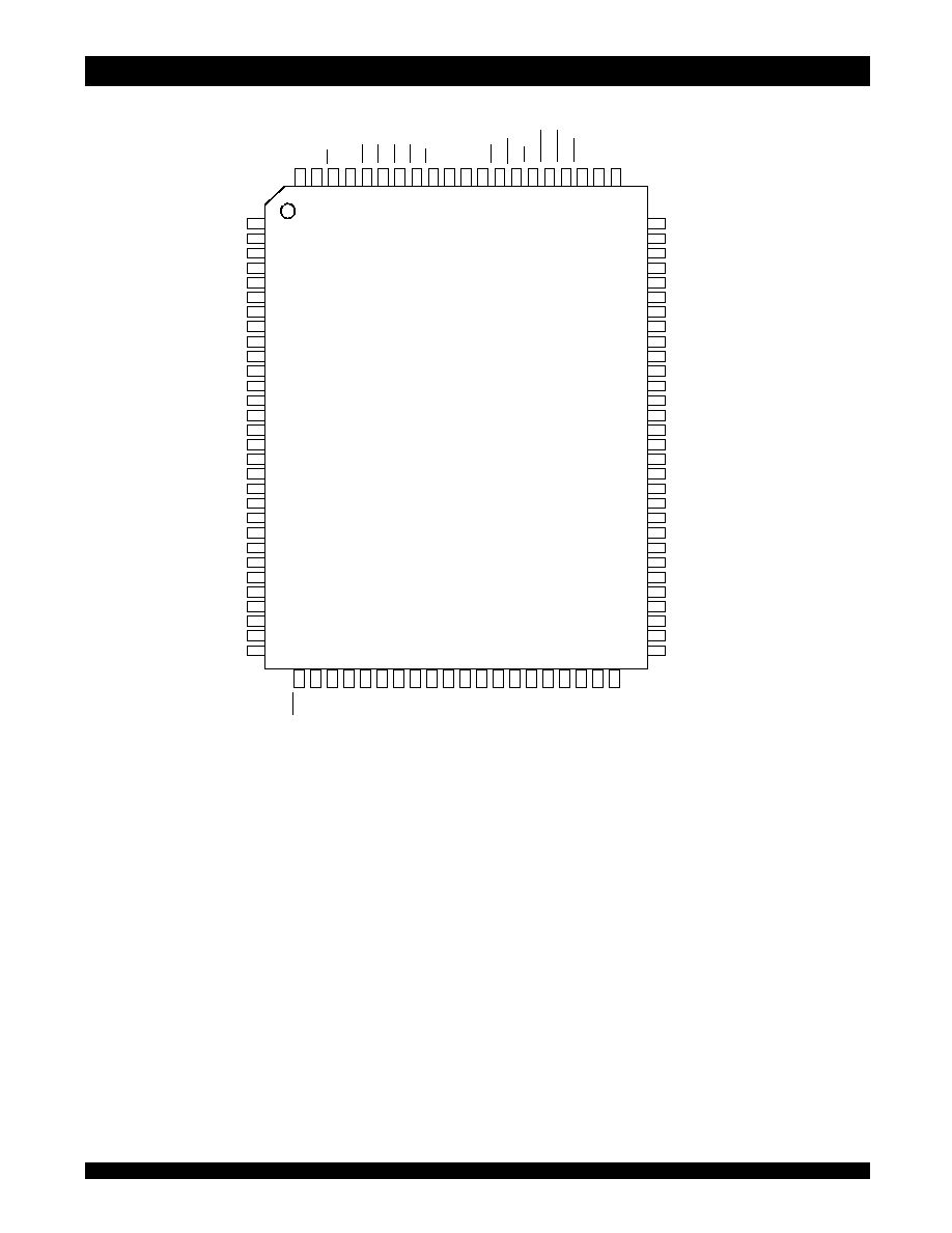
Pin Configuration 256K x 36, 100-Pin TQFP
NOTES:
1. Pin 14 can either be directly connected to V
DD
, or connected to an input voltage
V
IH
, or left unconnected.
2. Pin
64 can be left unconnected and the device will always remain in active mode.
100 99 98 97 96 95 94 93 92 91 90
87 86 85 84 83 82 81
89 88
1
2
3
4
5
6
7
8
9
10
11
12
13
14
15
16
17
18
19
20
21
22
23
24
25
26
27
28
29
30
A
6
A
7
C
E
C
S
0
B
W
4
B
W
3
B
W
2
B
W
1
C
S
1
V
D
D
V
S
S
C
LK
G
W
B
W
E
O
E
A
D
S
C
A
D
S
P
A
D
V
A
8
A
9
31 32 33 34 35 36 37 38 39 40 41 42 43 44 45 46 47 48 49 50
A
17
N
C
N
C
N
C
LB
O
A
14
A
13
A
12
A
11
A
10
V
D
D
V
S
S
A
0
A
1
A
2
A
3
A
4
A
5
I/O
31
I/O
30
V
DDQ
V
SS
I/O
29
I/O
28
I/O
27
I/O
26
V
SS
V
DDQ
I/O
25
I/O
24
V
SS
V
DD
I/O
23
I/O
22
V
DDQ
V
SS
I/O
21
I/O
20
I/O
19
I/O
18
V
SS
V
DDQ
I/O
17
I/O
16
80
79
78
77
76
75
74
73
72
71
70
69
68
67
66
65
64
63
62
61
60
59
58
57
56
55
54
53
52
51
I/O
14
V
DDQ
V
SS
I/O
13
I/O
12
I/O
11
I/O
10
V
SS
V
DDQ
I/O
9
I/O
8
V
SS
V
DD
I/O
7
I/O
6
V
DDQ
V
SS
I/O
5
I/O
4
I/O
3
I/O
2
V
SS
V
DDQ
I/O
1
I/O
0
5311 drw 02
V
DD
/ NC
(1)
I/O
15
I/O
P3
NC
I/O
P4
A
15
A
16
I/O
P1
NC
I/O
P2
ZZ
(2)
,
Top View