 | –≠–ª–µ–∫—Ç—Ä–æ–Ω–Ω—ã–π –∫–æ–º–ø–æ–Ω–µ–Ω—Ç: 72125 | –°–∫–∞—á–∞—Ç—å:  PDF PDF  ZIP ZIP |

Integrated Device Technology, Inc.
INDUSTRIAL TEMPERATURE RANGE
DECEMBER 1999
©1999 Integrated Device Technology, Inc.
DSC-2665/-
1
FEATURES:
∑ 25ns parallel port access time, 35ns cycle time
∑ 45MHz serial output shift rate
∑ Wide x16 organization offering easy expansion
∑ Low power consumption (50mA typical)
∑ Least/Most Significant Bit first read selected by asserting
the FL/DIR pin
∑ Four memory status flags: Empty, Full, Half-Full, and
Almost-Empty/Almost-Full
∑ Dual-Port zero fall-through architecture
∑ Available in 28-pin 300 mil plastic DIP and 28-pin SOIC
∑ Industrial temperature range (≠40
∞
C to +85
∞
C)
DESCRIPTION:
The IDT72105/72115/72125s are very high-speed, low-
power,dedicated, parallel-to-serial FIFOs. These FIFOs
possess a 16-bit parallel input port and a serial output port with
256, 512 and 1,024 word depths, respectively.
The ability to buffer wide word widths (x16) make these
FIFOs ideal for laser printers, FAX machines, local area
CMOS PARALLEL-TO-SERIAL FIFO
256 x 16, 512 x 16, 1,024 x 16
IDT72105
IDT72115
IDT72125
The IDT logo is a registered trademark of Integrated Device Technology, Inc.
FAST is a trademark of National Semiconductor Co.
networks (LANs), video storage and disk/tape controller ap-
plications.
Expansion in width and depth can be achieved using
multiple chips. IDT's unique serial expansion logic makes this
possible using a minimum of pins.
The unique serial output port is driven by one data pin (SO)
and one clock pin (SOCP). The Least Significant or Most
Significant Bit can be read first by programming the DIR pin
after a reset.
Monitoring the FIFO is eased by the availability of four
status flags: Empty, Full, Half-Full and Almost-Empty/Almost-
Full. The Full and Empty flags prevent any FIFO data overflow
or underflow conditions. The Half-Full Flag is available in both
single and expansion mode configurations. The Almost-
Empty/Almost-Full Flag is available only in a single device
mode.
The IDT72105/72115/72125 are fabricated using IDT's
leading edge, submicron CMOS technology. Military grade
product is manufactured in compliance with the latest revision
of Mil-STD-883, Class B.
FUNCTIONAL BLOCK DIAGRAM
2665 drw 01
RESET
LOGIC
FLAG
LOGIC
SERIAL OUTPUT
LOGIC
WRITE
POINTER
RAM
ARRAY
256 x 16
512 x 16
1,024 x 16
READ
POINTER
D
0≠15
16
EXPANSION
LOGIC
RSIX
RSOX
/DIR
SOCP
SO
For latest information contact IDT's web site at www.idt.com or fax-on-demand at 408-492-8391.

2
INDUSTRIAL TEMPERATURE RANGE
IDT72105/72115/72125 PARALLEL-TO-SERIAL CMOS FIFO
256 x 16, 512 x 16, 1,024 x 16
PIN CONFIGURATION
PIN DESCRIPTIONS
PLASTIC THIN DIP (P28-2, order code: TP)
SOIC (SO28-3, order code: SO)
TOP VIEW
5
6
7
8
9
10
11
12
13
D
2
D
3
D
4
GND
1
2
3
4
14
28
27
26
25
24
23
22
21
RSOX/
/DIR
Vcc
SO
SOCP
20
19
18
17
16
15
D
1
D
0
D
13
D
14
D
15
D
12
RSIX
D
5
D
6
D
7
D
9
D
10
D
11
D
8
2665 drw 02
Symbol
Name
I/O
Description
D
0
≠D
15
Inputs
I
Data inputs for 16-bit wide data.
RS
Reset
I
When
RS
is set low, internal READ and WRITE pointers are set to the first location of the RAM
array.
FF
and
HF
go HIGH.
EF
and
AEF
go LOW. A reset is required before an initial WRITE
after power-up.
W
must be high during the
RS
cycle. Also the First Load pin (
FL
) is programmed
only during Reset.
W
Write
I
A write cycle is initiated on the falling edge of WRITE if the Full Flag (
FF
) is not set. Data set-up
and hold times must be adhered to with respect to the rising edge of WRITE. Data is stored in the
RAM array sequentially and independently of any ongoing read operation.
SOCP
Serial Output
Clock
I
A serial bit read cycle is initiated on the rising edge of SOCP if the Empty Flag (
EF
) is not set. In
both Depth and Serial Word Width Expansion modes, all of the SOCP pins are tied together.
FL
/DIR
First Load/
Direction
I
This is a dual purpose input used in the width and depth expansion configurations. The First
Load (
FL
) function is programmed only during Reset (
RS
) and a LOW on
FL
indicates the first
device to be loaded with a byte of data. All other devices should be programmed HIGH. The
Direction (DIR) pin controls shift direction after Reset and tells the device whether to read out the
Least Significant or Most Significant bit first.
RSIX
Read Serial In
Expansion
I
In the single device configuration, RSIX is set HIGH. In depth expansion or daisy chain
expansion, RSIX is connected to RSOX (expansion out) of the previous device.
SO
Serial Output
O
Serial data is output on the Serial Output (SO) pin. Data is clocked out LSB or MSB depending
on the Direction pin programming. During Expansion the SO pins are tied together.
FF
Full Flag
O
When
FF
goes LOW, the device is full and further WRITE operations are inhibited. When
FF
is
HIGH, the device is not full.
EF
Empty Flag
O
When
EF
goes LOW, the device is empty and further READ operations are inhibited. When
EF
is
HIGH, the device is not empty.
HF
Half-Full Flag
O
When
HF
is LOW, the device is more than half-full. When
HF
is HIGH, the device is empty to
half-full.
RSOX/
AEF
Read Serial
Out Expansion
Almost-Empty,
Almost-Full
Flag
O
This is a dual purpose output. In the single device configuration (RSIX HIGH), this is an
AEF
output pin. When
AEF
is LOW, the device is empty-to-(1/8 full -1) or (7/8 full +1)-to-full. When
AEF
is HIGH, the device is 1/8-full up to 7/8-full. In the Expansion configuration (RSOX
connected to RSIX of the next device) a pulse is sent from RSOX to RSIX to coordinate the
width, depth or daisy chain expansion.
V
CC
Power Supply
Single power supply of 5V.
GND
Ground
Single ground of 0V.
2665 tbl 01
3
INDUSTRIAL TEMPERATURE RANGE
IDT72105/72115/72125 PARALLEL-TO-SERIAL CMOS FIFO
256 x 16, 512 x 16, 1,024 x 16
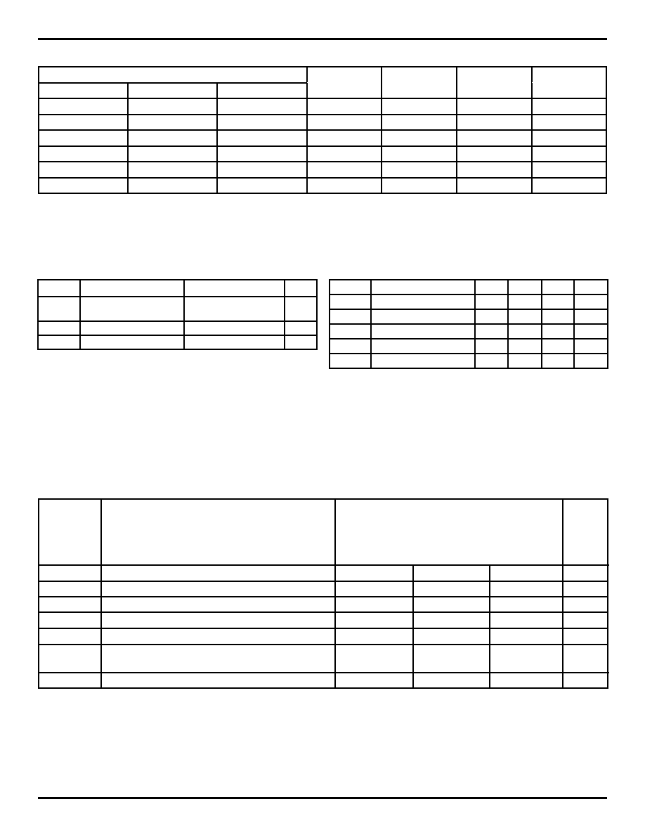
Number of Words in FIFO
IDT72105
IDT72115
IDT72125
F
F
F
FFFFF
A
A
A
AEEEEFFFF
H
H
H
HFFFF
E
E
E
EFFFF
0
0
0
H
L
H
L
1≠31
1≠63
1≠127
H
L
H
H
32≠128
64≠256
128≠512
H
H
H
H
129≠224
257≠448
513≠896
H
H
L
H
225≠255
449≠511
897≠1023
H
L
L
H
256
512
1024
L
L
L
H
2665 tbl 02
STATUS FLAGS
ABSOLUTE MAXIMUM RATINGS
(1)
RECOMMENDED DC OPERATING
CONDITIONS
Symbol
Rating
Commercial
Unit
V
TERM
Terminal Voltage with
≠0.5 to +7.0
V
Respect to GND
T
STG
Storage Temperature
≠55 to +125
∞
C
I
OUT
DC Output Current
≠50 to +50
mA
NOTE:
2665 tbl 03
1. Stresses greater than those listed under ABSOLUTE MAXIMUM
RATINGS may cause permanent damage to the device. This is a stress
rating only and functional operation of the device at these or any other
conditions above those indicated in the operational sections of this
specification is not implied. Exposure to absolute maximum rating
conditions for extended periods may affect reliability.
Symbol
Parameter
Min.
Typ.
Max.
Unit
V
CC
Supply Voltage
4.5
5.0
5.5
V
GND
Supply Voltage
0
0
0
V
V
IH
Input HIGH Voltage
2.0
--
--
V
V
IL
(1)
Input LOW Voltage
--
--
0.8
V
T
A
Operating Temperature
-40
--
+85
∞
C
NOTE:
2665 tbl 04
1. 1.5V undershoots are allowed for 10ns once per cycle.
DC ELECTRICAL CHARACTERISTICS
(Industrial: V
CC
= 5.0V
±
10%, T
A
= -40
∞
C to +85
∞
C)
NOTES:
2665 tbl 05
1. Measurements with 0.4V
V
IN
V
CC.
2. SOCP = V
IL
, 0.4
V
OUT
V
CC
.
3. For SO, I
OUT
= ≠4mA.
4. For SO, I
OUT
= 16mA.
5. Tested with outputs open (I
OUT
= 0).
6.
RS
=
FL
/DIR =
W
= V
CC
- 0.2V; SOCP = 0.2V; all other inputs = V
CC
- 0.2.
7. Measurements are made after reset.
IDT72105
IDT72115
IDT72125
Industrial
Symbol
Parameter
Min.
Typ.
Max.
Unit
I
LI
(1)
Input Leakage Current (Any Input)
≠1
--
1
µ
A
I
LO
(2)
Output Leakage Current
≠10
--
10
µ
A
V
OH
Output Logic "1" Voltage I
OUT
= ≠2mA
(3)
2.4
--
--
V
V
OL
Output Logic "0" Voltage I
OUT
= 8mA
(4)
--
--
0.4
V
I
CC1
(5)
Active Power Supply Current
--
50
100
mA
I
CC2
(5,6,7)
Standby Current
--
4
8
mA
(
W
=
RS
=
FL
/DIR = VIH; SOCP = VIL)
I
CC3
(5,6,7)
Power Down Current
--
1
6
mA

4
INDUSTRIAL TEMPERATURE RANGE
IDT72105/72115/72125 PARALLEL-TO-SERIAL CMOS FIFO
256 x 16, 512 x 16, 1,024 x 16
NOTE:
2665 tbl 06
1. Values guaranteed by design.
AC ELECTRICAL CHARACTERISTICS
(Industrial: V
CC
= 5V
±
10%, T
A
= -40
∞
C to +85
∞
C)
INDUSTRIAL
7 2 1 0 5 L 2 5
7 2 1 0 5 L 5 0
7 2 1 1 5 L 2 5
7 2 1 1 5 L 5 0
7 2 1 2 5 L 2 5
7 2 1 2 5 L 5 0
Symbol
P a r a m e t e r
Figure
M i n .
M a x .
M i n .
M a x .
Unit
t
S
Parallel Shift Frequency
--
--
28.5
--
15
MHz
t
SOCP
Serial Shift Frequency
--
--
50
--
40
MHz
PARALLEL INPUT TIMINGS
t
W C
Write Cycle Time
2
35
--
65
--
ns
t
W P W
Write Pulse Width
2
25
--
50
--
ns
t
W R
Write Recovery Time
2
10
--
15
--
ns
t
DS
Data Set-up Time
2
12
--
15
--
ns
t
DH
Data Hold Time
2
0
--
2
--
ns
t
WEF
Write High to
EF
HIGH
5, 6
--
35
--
45
ns
t
WFF
Write Low to
FF
LOW
4, 7
--
35
--
45
ns
t
WF
Write Low to Transitioning
HF
,
AEF
8
--
35
--
45
ns
t
WPF
Write Pulse Width After
FF
HIGH
7
25
--
50
--
ns
SERIAL OUTPUT TIMINGS
t
SOCP
Serial Clock Cycle Time
3
20
--
25
--
ns
t
SOCW
Serial Clock Width HIGH/LOW
3
8
--
10
--
ns
t
SOPD
SOCP Rising Edge to SO Valid Data
3
--
14
--
15
ns
t
SOHZ
SOCP Rising Edge to SO at High-Z
(1)
3
3
14
3
15
ns
t
SOLZ
SOCP Rising Edge to SO at Low-Z
(1)
3
3
14
3
15
ns
t
SOCEF
SOCP Rising Edge to
EF
LOW
5, 6
--
35
--
45
ns
t
SOCFF
SOCP Rising Edge to
FF
HIGH
4, 7
--
35
--
45
ns
t
SOCF
SOCP Rising Edge to Transitioning
HF
,
AEF
8
--
35
--
45
ns
t
REFSO
SOCP Delay After
EF
HIGH
6
35
--
65
--
ns
RESET TIMINGS
t
RSC
Reset Cycle Time
1
35
--
65
--
ns
t
RS
Reset Pulse Width
1
25
--
50
--
ns
t
RSS
Reset Set-up Time
1
25
--
50
--
ns
t
RSR
Reset Recovery Time
1
10
--
15
--
ns
EXPANSION MODE TIMINGS
t
FLS
FL
Set-up Time to
RS
Rising Edge
9
7
--
8
--
ns
t
FLH
FL
Hold Time to
RS
Rising Edge
9
0
--
2
--
ns
t
DIRS
DIR Set-up Time to SOCP Rising Edge
9
10
--
12
--
ns
t
DIRH
DIR Hold Time from SOCP Rising Edge
9
5
--
5
--
ns
t
SOXD1
SOCP Rising Edge to RSOX Rising
Edge
9
--
15
--
17
ns
t
SOXD2
SOCP Rising Edge to RSOX Falling
Edge
9
--
15
--
17
ns
t
SIXS
RSIX Set-up Time to SOCP Rising
Edge
9
5
--
8
--
ns
t
SIXPW
RSIX Pulse Width
9
10
--
15
--
ns

5
INDUSTRIAL TEMPERATURE RANGE
IDT72105/72115/72125 PARALLEL-TO-SERIAL CMOS FIFO
256 x 16, 512 x 16, 1,024 x 16
AC TEST CONDITIONS
2665 tbl 07
NOTES:
1.
EF
,
FF
,
HF
and
AEF
may change status during Reset, but flags will be valid at t
RSC.
2. SOCP should be in the steady LOW or HIGH during t
RSS
. The first LOW-HIGH (or HIGH-LOW) transition can begin after t
RSR
.
Figure 1. Reset
FUNCTIONAL DESCRIPTION
Parallel Data Input
The device must be reset before beginning operation so
that all flags are set to their initial state. In width or depth
expansion the First Load pin (
FL
) must be programmed to
indicate the first device.
The data is written into the FIFO in parallel through the D
0≠
15
input data lines. A write cycle is initiated on the falling edge
of the Write (
W
) signal provided the Full Flag (
FF
) is not
asserted. If the
W
signal changes from HIGH-to-LOW and the
Full Flag (
FF
) is already set, the write line is internally inhibited
internally from incrementing the write pointer and no write
operation occurs.
Data set-up and hold times must be met with respect to the
rising edge of Write. On the rising edge of
W
, the write pointer
is incremented. Write operations can occur simultaneously or
asynchronously with read operations.
Serial Data Output
The serial data is output on the SO pin. The data is clocked
out on the rising edge of SOCP providing the Empty Flag (
EF
)
is not asserted. If the Empty Flag is asserted then the next data
word is inhibited from moving to the output register and being
clocked out by SOCP.
The serial word is shifted out Least Significant Bit or Most
Significant Bit first, depending on the
FL
/DIR level during
operation. A LOW on DIR will cause the Least Significant Bit
to be read out first. A HIGH on DIR will cause the Most
Significant Bit to be read out first.
CAPACITANCE
(T
A
= +25
∞
C, f = 1.0MHz)
Symbol
Parameter
(1)
Conditions
Max.
Unit
C
IN
Input Capacitance
V
IN
= 0V
10
pF
C
OUT
Output
Capacitance
V
OUT
= 0V
12
pF
NOTE:
2665 tbl 08
1. Characterized values, not currently tested.
Input Pulse Levels
GND to 3.0V
Input Rise/Fall Times
5ns
Input Timing Reference Levels
1.5V
Output Reference Levels
1.5V
Output Load
See Figure A
2665 drw 03
1.1K
30pF
680
5V
TO
OUTPUT
PIN
*
or equivalent circuit
Figure A. Output Load
*Includes jig and scope capacitances.
t
RSC
,
,
FLAG
STABLE
FLAG
STABLE
2665 drw 04
t
RSC
t
RSS
t
RSR
t
RSC
t
RS
SOCP
t
RSS
t
RSR
NOTE 2
t
FLS
t
FLH
/DIR