 | –≠–ª–µ–∫—Ç—Ä–æ–Ω–Ω—ã–π –∫–æ–º–ø–æ–Ω–µ–Ω—Ç: 72141 | –°–∫–∞—á–∞—Ç—å:  PDF PDF  ZIP ZIP |
1
FEBRUARY 2002
©
2002 Integrated Device Technology, Inc. All rights reserved. Product specifications subject to change without notice.
CMOS PARALLEL-TO-SERIAL FIFO
2,048 x 9 and 4,096 x 9
IDT72131
IDT72141
DSC-2751/1
IDT and the IDT logo are registered trademarks of Integrated Device Technology, Inc
INDUSTRIAL TEMPERATURE RANGE
FEATURES:
∑
35ns parallel port access time, 45ns cycle time
∑
50MHz serial port shift rate
∑
Expandable in depth and width with no external components
∑
Programmable word lengths including 7-9, 16-18, 32-36 bit using
Flexishift
TM
serial output without using any additional components
∑
Multiple status flags: Full, Almost-Full (1/8 from full), Half-Full,
Almost- Empty (1/8 from empty), and Empty
∑
Asynchronous and simultaneous read and write operations
∑
Dual-Port zero fall-through architecture
∑
Retransmit capability in single device mode
∑
Produced with high-performance, low power CMOS technology
∑
Available in 28-pin plastic DIP
∑
Industrial temperature range (≠40
∞
C to +85
∞
C)
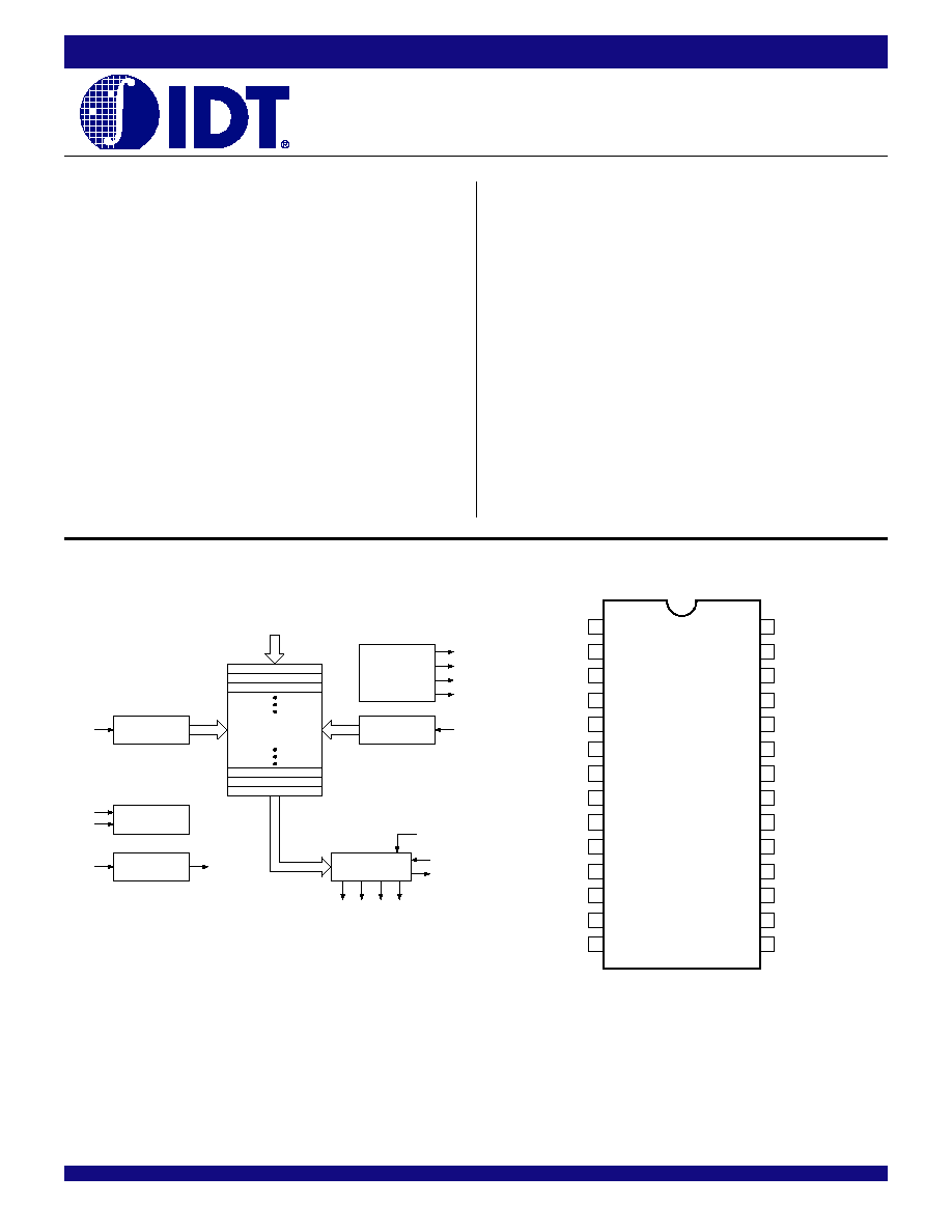
FUNCTIONAL BLOCK DIAGRAM
PIN CONFIGURATION
DESCRIPTION:
The IDT72131/72141 are high-speed, low power parallel-to-serial FIFOs.
These FIFOs are ideally suited to serial communications applications, tape/
disk controllers, and local area networks (LANs). These devices can be
configured with the IDTs serial-to-parallel FIFOs (IDT72132/72142) for
bidirectional serial data buffering.
The FIFO has a 9-bit parallel input port and a serial output port. Wider
and deeper parallel-to-serial data buffers can be built using multiple
IDT72131/72141 chips. IDTs unique Flexishift serial expansion logic (SOX,
NR) makes width expansion possible with no additional components. These
FIFOs will expand to a variety of word widths including 8, 9, 16, and 32 bits.
These devices can also be directly connected for depth expansion.
Five flags are provided to monitor the FIFO. The full and empty flags
prevent any FIFO data overflow or underflow conditions. The Almost-Full
(7/8), Half-Full, and Almost-Empty (1/8) flags signal memory utilization
within the FIFO.
The IDT72131/72141 is fabricated using IDTs high-speed submicron
CMOS technology.
2751 drw01
D
0
-D
8
RAM ARRAY
2,048 x 9
4,096 x 9
WRITE
POINTER
NEXT READ
POINTER
FLAG
LOGIC
EF
AEF
/
HF
FF
NR
W
RESET LOGIC
RS
EXPANSION
LOGIC
XI
FL
/
RT
XO
/
SERIAL OUTPUT
CIRCUITRY
SOCP
SOX
SO
Q
4
Q
6
Q
7
Q
8
5
6
7
8
9
10
11
12
FF
W
D
4
D
3
1
2
3
4
26
25
24
23
22
21
20
19
Vcc
18
17
16
15
D
2
D
1
XI
SOX
FL
/
RT
RS
EF
XO
/
HF
SOCP
SO
AEF
GND
13
14
28
27
Q
4
GND
NR
2751 drw02
D
0
D
5
D
6
D
7
D
8
Q
7
Q
8
Q
6
PLASTIC DIP (P28-1, order code: P)
TOP VIEW

2
IDT72131/72141 CMOS PARALLEL-TO-SERIAL FIFO
2,048 x 9 and 4,096 x 9
INDUSTRIAL TEMPERATURE RANGE
Symbol
Name
I/O
Description
D
0
≠D
8
Inputs
I
Data inputs for 9-bit wide data.
RS
Reset
I
When
RS is set LOW, internal READ and WRITE pointers are set to the first location of the RAM array. HF
and
FF go HIGH, and AEF and EF go LOW. A reset is required before an initial WRITE after power-up.
W must be HIGH and SOCP must be LOW during RS cycle.
W
Write
I
A write cycle is initiated on the falling edge of WRITE if the Full Flag (
FF) is not set. Data set-up and hold
times must be adhered to with respect to the rising edge of WRITE. Data is stored in the RAM array
sequentially and independently of any ongoing read operation.
SOCP
Serial Output
I
A serial bit read cycle is initiated on the rising edge of SOCP if the Empty Flag (
EF) is not set. In both Depth
Clock
and Serial Word Width Expansion modes, all of the SOCP pins are tied together.
NR
Next Read
I
To program the Serial Out data word width , connect
NR with one of the Data Set pins (Q
4
, Q
6
, Q
7
and Q
8
).
For example,
NR - Q
7
programs for a 8-bit Serial Out word width.
FL/RT
First Load/
I
This is a dual purpose input. In the single device configuration (
XI grounded), activating retransmit (FL/RT-
Retransmit
LOW) will set the internal READ pointer to the first location. There is no effect on the WRITE pointer.
W must
be high and SOCP must be low before setting
FL/RT LOW. Retransmit is not compatible with depth
expansion. In the depth expansion configuration,
FL/RT grounded indicates the first activated device.
XI
Expansion In
I
In the single device configuration,
XI is grounded. In depth expansion or daisy chain expansion, XI is
connected to
XO (expansion out) of the previous device.
SOX
Serial Output
I
In the Serial Output Expansion mode, the SOX pin of the least significant device is tied HIGH. The SOX pin
Expansion
of all other devices is connected to the Q
8
pin of the previous device. Data is then clocked out least significant
bit first. For single device operation, SOX is tied HIGH.
SO
Serial Output
O
Serial data is output on the Serial Output (SO) pin. Data is clocked out Least Significant Bit first. In the Serial
Width Expansion mode the SO pins are tied together and each SO pin is tristated at the end of the byte.
FF
Full Flag
O
When
FF goes LOW, the device is full and further WRITE operations are inhibited. When FF is HIGH, the
device is not full.
EF
Empty Flag
O
When
EF goes LOW, the device is empty and further READ operations are inhibited. When EF is HIGH, the
device is not empty. See the description on page 6 for more details.
AEF
Almost-Empty/
O
When
AEF is LOW, the device is empty to 1/8 full or 7/8 to completely full. When AEF is HIGH, the device
Almost-Full Flag
is greater than 1/8 full, but less than 7/8 full.
XO/HF
Expansion Out/
O
This is a dual-purpose output. In the single device configuration (
XI grounded), the device is more than half
Half-Full Flag
full when
HF is LOW. In the depth expansion configuration (XO connected to XI of the next device), a pulse
is sent from
XO to XI when the last location in the RAM array is filled.
Q
4
, Q
6
,
Data Set
O
The appropriate Data Set pin (Q
4
, Q
6
, Q
7
and Q
8
) is connected to
NR to program the Serial Out data word
Q
7
and Q
8
width. For example: Q
6
-
NR programs a 7-bit word width, Q
8
-
NR programs a 9-bit word width, etc.
V
CC
Power Supply
Single Power Supply of 5V.
GND
Ground
Single ground at 0V.
PIN DESCRIPTIONS
Number of Words in FIFO
IDT72131
IDT72141
FF
AEF
HF
EF
0
0
H
L
H
L
1-255
1-511
H
L
H
H
256-1,024
512-2,048
H
H
H
H
1,025-1,792
2,049-3,584
H
H
L
H
1,793-2,047
3,585-4,095
H
L
L
H
2,048
4,096
L
L
L
H
STATUS FLAGS

3
IDT72131/72141 CMOS PARALLEL-TO-SERIAL FIFO
2,048 x 9 and 4,096 x 9
INDUSTRIAL TEMPERATURE RANGE
ABSOLUTE MAXIMUM RATINGS
(1)
Symbol
Rating
Commercial
Unit
V
TERM
Terminal Voltage with
≠0.5 to +7.0
V
Respect to GND
T
STG
Storage
≠55 to +125
∞
C
Temperature
I
OUT
DC Output Current
≠50 to +50
mA
NOTE:
1.
Stresses greater than those listed under ABSOLUTE MAXIMUM RATINGS may cause
permanent damage to the device. This is a stress rating only and functional operation of
the device at these or any other conditions above those indicated in the operational
sections of this specification is not implied. Exposure to absolute maximum rating
conditions for extended periods may affect reliability.
RECOMMENDED OPERATING
CONDITIONS
Symbol
Parameter
Min.
Typ.
Max.
Unit
V
CC
Commercial Supply
4.5
5.0
5.5
V
Voltage
GND
Supply Voltage
0
0
0
V
V
IH
Input High Voltage
2.0
--
--
V
Commercial
V
IL
(1)
Input Low Voltage
--
--
0.8
V
T
A
Operating Temperature
-40
--
85
∞
C
Industrial
NOTE:
1.
1.5V undershoots are allowed for 10ns once per cycle.
DC ELECTRICAL CHARACTERISTICS
(Industrial: V
CC
= 5.0V ± 10%, T
A
= -40
∞
C to +85
∞
C)
IDT72131
IDT72141
Industrial
Symbol
Parameter
Min.
Typ.
Max.
Unit
I
IL
(1)
Input Leakage Current
≠1
--
1
µ A
(Any Input)
I
OL
(2)
Output Leakage Current
≠10
--
10
µ A
V
OH
Output Logic "1" Voltage,
2.4
--
--
V
I
OUT
= ≠2mA
V
OL
Output Logic "0" Voltage
--
--
0.4
V
I
OUT
= 8mA
I
CC1
(3)
Active Power Supply Current
--
90
140
mA
I
CC2
(3,4)
Standby Current
--
8
12
mA
(
W = RS = FL/RT = V
IH
; SOCP = V
IL
)
I
CC3
(3,4)
Power Down Current
--
--
2
mA
CAPACITANCE
(T
A
= +25
∞
C, f = 1.0MHz)
Symbol
Parameter
Conditions
Max.
Unit
C
IN
Input Capacitance
V
IN
= 0V
10
pF
C
OUT
Output Capacitance
V
OUT
= 0V
12
pF
NOTE:
1.
Characterized values, not currently tested.
NOTES:
1. Measurements with 0.4
V
IN
V
CC
.
2. SOCP
V
IL
, 0.4
V
OUT
V
CC
.
3. Tested with outputs open (I
OUT
= 0).
4.
RS = FL/RT = W = V
CC
-0.2V; SOCP
0.2V; all other inputs = V
CC
- 0.2V or GND + 0.2V, which toggle at 20 MHz.

4
IDT72131/72141 CMOS PARALLEL-TO-SERIAL FIFO
2,048 x 9 and 4,096 x 9
INDUSTRIAL TEMPERATURE RANGE
AC ELECTRICAL CHARACTERISTICS
(Industrial: V
CC
= 5.0V ± 10%, T
A
= -40
∞
C to +85
∞
C)
Industrial
IDT72131L35
IDT72131L50
IDT72141L35
IDT72141L50
Symbol
Parameter
Min.
Max.
Min.
Max.
Unit
t
S
Parallel Shift Frequency
--
22.2
--
15
MHz
t
SOCP
Serial-Out Shift Frequency
--
50
--
40
MHz
PARALLEL INPUT TIMINGS
t
DS
Data Set-up Time
18
--
30
--
ns
t
DH
Data Hold Time
0
--
5
--
ns
t
WC
Write Cycle Time
45
--
65
--
ns
t
WPW
Write Pulse Width
35
--
50
--
ns
t
WR
Write Recovery Time
10
--
15
--
ns
t
WEF
Write High to
EF HIGH
--
30
--
45
ns
t
WFF
Write Low to
FF LOW
--
30
--
45
ns
t
WF
Write Low to Transitioning
HF, AEF
--
45
--
65
ns
t
WPF
Write Pulse Width After
FF HIGH
35
--
50
--
ns
SERIAL OUTPUT TIMINGS
t
SOHZ
SOCP Rising Edge to SO at High-Z
(1)
5
16
5
26
ns
t
SOLZ
SOCP Rising Edge to SO at Low-Z
(1)
5
22
5
22
ns
t
SOPD
SOCP Rising Edge to Valid Data on SO
--
18
--
18
ns
t
SOX
SOX Set-up Time to SOCP Rising Edge
5
--
5
--
ns
t
SOCW
Serial In Clock Width HIGH/LOW
8
--
10
--
ns
t
SOCEF
SOCP Rising Edge (Bit 0 - Last Word) to
EF LOW
--
20
--
25
ns
t
SOCFF
SOCP Rising Edge to
FF HIGH
--
30
--
40
ns
t
SOCF
SOCP Rising Edge to
HF, AEF, HIGH
--
30
--
40
ns
t
REFSO
Recovery Time SOCP After
EF HIGH
35
--
50
--
ns
RESET TIMINGS
t
RSC
Reset Cycle Time
45
--
65
--
ns
t
RS
Reset Pulse Width
35
--
50
--
ns
t
RSS
Reset Set-up Time
35
--
50
--
ns
t
RSR
Reset Recovery Time
10
--
15
--
ns
t
RSF1
Reset to
EF and AEF LOW
--
45
--
65
ns
t
RSF2
Reset to
HF and FF HIGH
--
45
--
65
ns
t
RSQL
Reset to Q LOW
20
--
35
--
ns
t
RSQH
Reset to Q HIGH
20
--
35
--
ns
RETRANSMIT TIMINGS
t
RTC
Retransmit Cycle Time
45
--
65
--
ns
t
RT
Retransmit Pulse Width
35
--
50
--
ns
t
RTS
Retransmit Set-up Time
35
--
50
--
ns
t
RTR
Retransmit Recovery Time
10
--
15
--
ns
DEPTH EXPANSION MODE TIMINGS
t
XOL
Read/Write to
XO LOW
--
35
--
50
ns
t
XOH
Read/Write to
XO HIGH
--
35
--
50
ns
t
XI
XI Pulse Width
35
--
50
--
ns
t
XIR
XI Recovery Time
10
--
10
--
ns
t
XIS
XI Set-up Time
15
--
15
--
ns
NOTE:
1. Guaranteed by design minimum times, not tested.

5
IDT72131/72141 CMOS PARALLEL-TO-SERIAL FIFO
2,048 x 9 and 4,096 x 9
INDUSTRIAL TEMPERATURE RANGE
AC TEST CONDITIONS
Input Pulse Levels
GND to 3.0V
Input Rise/Fall Times
5ns
Input Timing Reference Levels
1.5V
Output Reference Levels
1.5V
Output Load
See Figure A
or equivalent circuit
SERIAL DATA OUTPUT
The serial data is output on the SO pin. The data is clocked out on the
rising edge of SOCP providing the Empty Flag (
EF) is not asserted. If the
Empty Flag is asserted then the next data word is inhibited from moving to
the output register and being clocked out by SOCP. NOTE: SOCP should
not be clocked once the last bit of the last word has been clocked out. If it
is, then two things will occur. One, the SO pin will go High-Z and two, SOCP
will be out of sync with Next Read (
NR).
The serial word is shifted out Least Significant Bit first, that is the first bit
will be D0, then D1 and so on up to the serial word width. The serial word
width must be programmed by connecting the appropriate Data Set line
(Q4, Q6, Q7 or Q8) to the
NR input. The Data Set lines are taps off a digital
delay line. Selecting one of these taps, programs the width of the serial word
to be read and shifted out.
FUNCTIONAL DESCRIPTION
PARALLEL DATA INPUT
The data is written into the FIFO in parallel through the D0-8 input data
lines. A write cycle is initiated on the falling edge of the Write (
W) signal
provided the Full Flag (
FF) is not asserted. If the W signal changes from
HIGH-to-LOW and the Full-Flag (
FF) is already set, the write line is inhibited
internally from incrementing the write pointer and no write operation occurs.
Data set-up and hold times must be met with respect to the rising edge
of Write. The data is written to the RAM at the write pointer. On the rising
edge of
W, the write pointer is incremented. Write operations can occur
simultaneously or asynchronously with read operations.
*Including jig and scope capacitances
Figure A. Output Load
1.1K
30pF*
680
5V
D.U.T.
2751 drw03
Figure 1. Reset
2751 drw04
W
RS
AEF
,
EF
HF
,
FF
t
RSC
t
RS
t
RSS
t
RSR
t
RSF1
t
RSF2
t
RSS
t
RSR
t
RSQH
t
RSQL
SOCP
Q
4
, Q
6
, Q
7
, Q
8