 | –≠–ª–µ–∫—Ç—Ä–æ–Ω–Ω—ã–π –∫–æ–º–ø–æ–Ω–µ–Ω—Ç: 72225 | –°–∫–∞—á–∞—Ç—å:  PDF PDF  ZIP ZIP |
1
IDT72205LB/72215LB/72225LB/72235LB/72245LB CMOS SyncFIFOTM
256 x 18-BIT, 512 x 18, 1,024 x 18, 2,048 x 18 and 4,096 x 18
Commercial And Industrial Temperature Ranges
FEATURES:
∑ 256 x 18-bit organization array (IDT72205LB)
∑ 512 x 18-bit organization array (IDT72215LB)
∑ 1,024 x 18-bit organization array (IDT72225LB)
∑ 2,048 x 18-bit organization array (IDT72235LB)
∑ 4,096 x 18-bit organization array (IDT72245LB)
∑ 10 ns read/write cycle time
∑ Empty and Full flags signal FIFO status
∑ Easily expandable in depth and width
∑ Asynchronous or coincident read and write clocks
∑ Programmable Almost-Empty and Almost-Full flags with
default settings
∑ Half-Full flag capability
∑ Dual-Port zero fall-through time architecture
∑ Output enable puts output data bus in high-impedance
state
∑ High-performance submicron CMOS technology
∑ Available in a 64-lead thin quad flatpack (TQFP/STQFP)
and plastic leaded chip carrier (PLCC)
∑ Industrial temperature range (≠40
∞
C to +85
∞
C) is available
Integrated Device Technology, Inc.
IDT72205LB
IDT72215LB
IDT72225LB
IDT72235LB
IDT72245LB
CMOS SyncFIFOTM
256 x 18, 512 x 18, 1,024 x 18,
2,048 x 18 and 4,096 x 18
SyncFIFO is a trademark and the IDT logo is a registered trademark of Integrated Device Technology, Inc
COMMERCIAL AND INDUSTRIAL TEMPERATURE RANGES
MAY 2000
©2000 Integrated Device Technology, Inc.
DSC-2766/-
are applicable for a wide variety of data buffering needs, such
as optical disk controllers, Local Area Networks (LANs), and
interprocessor communication.
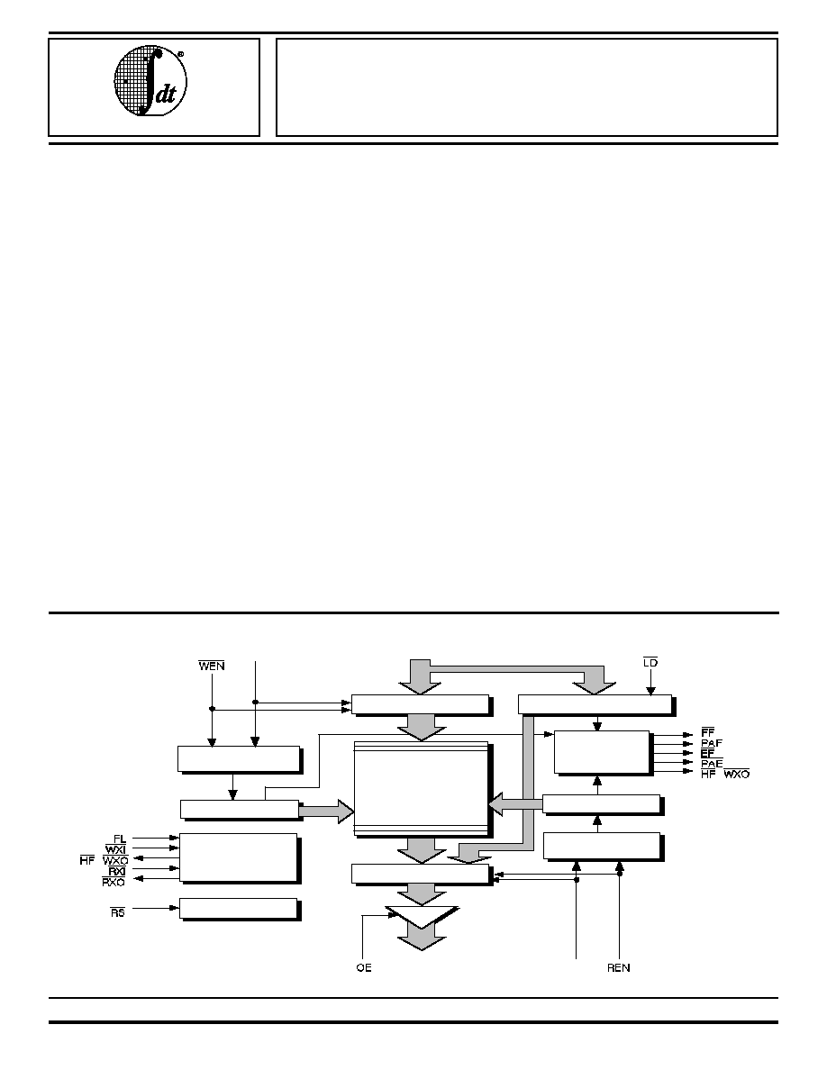
These FIFOs have 18-bit input and output ports. The input
port is controlled by a free-running clock (WCLK), and an input
enable pin (
WEN
). Data is read into the synchronous FIFO on
every clock when
WEN
is asserted. The output port is controlled
by another clock pin (RCLK) and another enable pin (
REN
). The
read clock can be tied to the write clock for single clock
operation or the two clocks can run asynchronous of one
another for dual-clock operation. An Output Enable pin (
OE
) is
provided on the read port for three-state control of the output.
The synchronous FIFOs have two fixed flags, Empty (
EF
) and
Full (
FF
), and two programmable flags, Almost-Empty (
PAE
)
and Almost-Full (
PAF
). The offset loading of the programmable
flags is controlled by a simple state machine, and is initiated by
asserting the Load pin (
LD
). A Half-Full flag (
HF
) is available
when the FIFO is used in a single device configuration.
These devices are depth expandable using a Daisy-Chain
technique. The XI and
XO
pins are used to expand the FIFOs.
In depth expansion configuration,
FL
is grounded on the first
device and set to HIGH for all other devices in the Daisy Chain.
The IDT72205LB/72215LB/72225LB/72235LB/72245LB is
fabricated using IDT's high-speed submicron CMOS technol-
ogy.
1
FUNCTIONAL BLOCK DIAGRAM
INPUT REGISTER
OUTPUT REGISTER
RAM ARRAY
256 x 18, 512 x 18
1,024 x 18, 2,048 x 18
4,096 x 18
∑
∑
∑
∑
OFFSET REGISTER
FLAG
LOGIC
/(
)
READ POINTER
READ CONTROL
LOGIC
WRITE CONTROL
LOGIC
WRITE POINTER
EXPANSION LOGIC
RESET LOGIC
WCLK
D0-D17
(
)/
RCLK
Q0-Q17
2766 drw 01
DESCRIPTION:
The IDT72205LB/72215LB/72225LB/72235LB/72245LB
are very high-speed, low-power First-In, First-Out (FIFO)
memories with clocked read and write controls. These FIFOs
For latest information contact IDT's web site at www.idt.com or fax-on-demand at 408-492-8391.
2
IDT72205LB/72215LB/72225LB/72235LB/72245LB CMOS SyncFIFOTM
256 x 18, 512 x 18, 1,024 x 18, 2,048 x 18 and 4,096 x 18
Commercial And Industrial Temperature Ranges
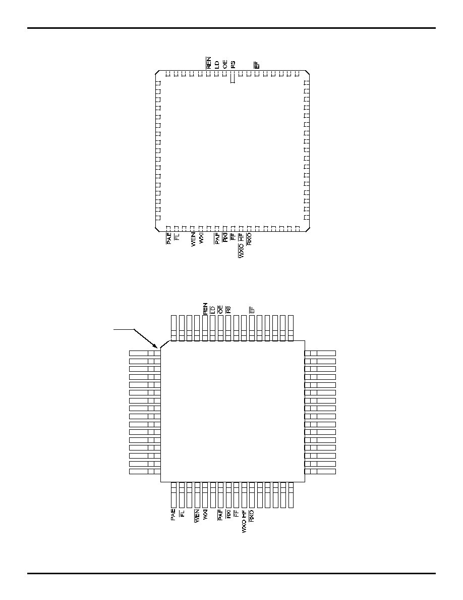
PIN CONFIGURATIONS
PLCC (J68-1, order code: J)
TOP VIEW
TQFP (PN64-1, order code: PF)
STQFP (PP64-1, order code: TF)
TOP VIEW
18
26
19
20
22
23
24
25
21
10
11
12
13
14
15
16
17
56
44
45
46
47
48
49
50
51
52
53
54
55
57
58
59
60
V
CC
Q
14
Q
13
GND
Q
12
Q
11
V
CC
Q
10
Q
9
GND
Q
8
Q
7
V
CC
Q
6
Q
5
GND
Q
4
D
14
D
13
D
12
D
11
D
10
D
9
V
CC
D
8
GND
D
7
D
6
D
5
D
4
D
3
D
2
D
1
D
0
1
9 8 7 6 5 4 3 2
68 67 66 65 64 63 62 61
27 28 29 30 31 32 33 34 35 36 37 38 39 40 41 42 43
2766 drw 02
D
15
D
16
V
CC
D
17
GND
RCLK
GND
V
CC
Q
17
Q
16
GND
Q
15
WCLK
V
CC
/
Q
0
Q
1
GND
Q
2
Q
3
V
CC
PIN 1
1
2
3
4
5
6
7
8
9
10
11
12
13
14
15
16
D
16
D
17
GND
RCLK
V
CC
GND
Q
17
Q
16
GND
Q
15
V
CC
Q
14
Q
13
GND
Q
12
Q
11
V
CC
Q
10
Q
9
GND
Q
8
Q
7
Q
6
Q
5
GND
Q
4
V
CC
48
47
46
45
44
43
42
41
40
39
38
37
36
35
34
33
D
15
D
14
D
13
D
12
D
11
D
10
D
9
D
8
D
7
D
6
D
5
D
4
D
3
D
2
D
1
D
0
WCLK
V
CC
/
Q
0
Q
1
GND
Q
2
Q
3
64
63
62
61
60
59
58
57
56
55
54
53
52
51
50
49
17
18
19
20
21
22
23
24
25
26
27
28
29
30
31
32
2766 drw 03
3
IDT72205LB/72215LB/72225LB/72235LB/72245LB CMOS SyncFIFOTM
256 x 18-BIT, 512 x 18, 1,024 x 18, 2,048 x 18 and 4,096 x 18
Commercial And Industrial Temperature Ranges
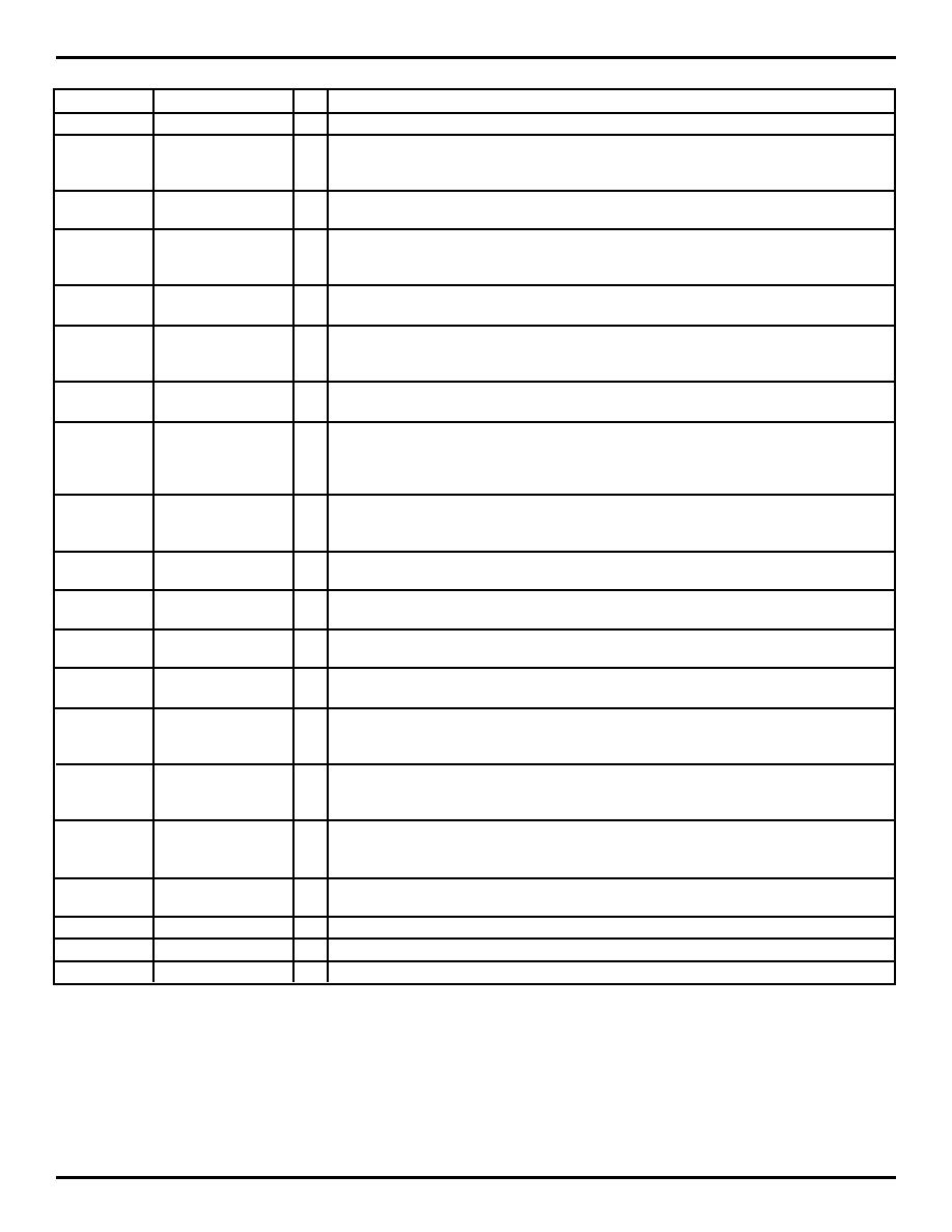
Symbol
Name
I/O
Description
D0≠D17
Data Inputs
I
Data inputs for a 18-bit bus.
RS
Reset
I
When
RS
is set LOW, internal read and write pointers are set to the first location of the
RAM array,
FF
and
PAF
go HIGH, and
PAE
and
EF
go LOW. A reset is required before an
initial WRITE after power-up.
WCLK
Write Clock
I
When
WEN
is LOW, data is written into the FIFO on a LOW-to-HIGH transition of WCLK,
if the FIFO is not full.
WEN
Write Enable
I
When
WEN
is LOW and
LD
is HIGH, data is written into the FIFO on every LOW-to-HIGH
transition of WCLK. When
WEN
is HIGH, the FIFO holds the previous data. Data will not be
written into the FIFO if the
FF
is LOW.
RCLK
Read Clock
I
When
REN
is LOW, data is read from the FIFO on a LOW-to-HIGH transition of RCLK, if the
FIFO is not empty.
REN
Read Enable
I
When
REN
is LOW and
LD
is HIGH, data is read from the FIFO on every LOW-to-HIGH
transition of RCLK. When
REN
is HIGH, the output register holds the previous data. Data will
not be read from the FIFO if the
EF
is LOW.
OE
Output Enable
I
When
OE
is LOW, the data output bus is active. If
OE
is HIGH, the output data bus will
be in a high-impedance state.
LD
Load
I
When
LD
is LOW, data on the inputs D0≠D11 is written to the offset and depth registers
on the LOW-to-HIGH transition of the WCLK, when
WEN
is LOW. When
LD
is LOW,
data on the outputs Q0≠Q11 is read from the offset and depth registers on the LOW-to-
HIGH transition of the RCLK, when
REN
is LOW.
FL
First Load
I
In the single device or width expansion configuration,
FL
is grounded. In the depth expansion
configuration,
FL
is grounded on the first device (first load device) and set to HIGH for all other
devices in the Daisy Chain.
WXI
Write Expansion
I
In the single device or width expansion configuration,
WXI
is grounded. In the depth
expansion configuration,
WXI
is connected to
WXO
(Write Expansion Out) of the previous device.
RXI
Read Expansion
I
In the single device or width expansion configuration,
RXI
is grounded. In the depth expansion
configuration,
RXI
is connected to
RXO
(Read Expansion Out) of the previous device.
FF
Full Flag
O
When
FF
is LOW, the FIFO is full and further data writes into the input are inhibited. When
FF
is HIGH, the FIFO is not full.
FF
is synchronized to WCLK.
EF
Empty Flag
O
When
EF
is LOW, the FIFO is empty and further data reads from the output are inhibited.
When
EF
is HIGH, the FIFO is not empty.
EF
is synchronized to RCLK.
PAE
Programmable
O
When
PAE
is LOW, the FIFO is almost empty based on the offset programmed into the
Almost-Empty Flag
FIFO. The default offset at reset is 31 from empty for IDT72205LB, 63 from empty for
IDT72215LB, and 127 from empty for IDT72225LB/72235LB/72245LB.
PAF
Programmable
O
When
PAF
is LOW, the FIFO is almost full based on the offset programmed into the FIFO.
Almost-Full Flag
The default offset at reset is 31 from full for IDT72205LB, 63 from full for IDT72215LB, and
127 from full for IDT72225LB/72235LB/72245LB.
WXO
/
HF
Write Expansion
O
In the single device or width expansion configuration, the device is more than half full
Out/Half-Full Flag
when
HF
is LOW. In the depth expansion configuration, a pulse is sent from
WXO
to
WXI
of the next device when the last location in the FIFO is written.
RXO
Read Expansion
O
In the depth expansion configuration, a pulse is sent from
RXO
to
RXI
of the next device
Out
when the last location in the FIFO is read.
Q0≠Q17
Data Outputs
O
Data outputs for a 18-bit bus.
V
CC
Power
+5V power supply pins.
GND
Ground
Eight ground pins for the PLCC and seven pins for the TQFP/STQFP.
PIN DESCRIPTION
4
IDT72205LB/72215LB/72225LB/72235LB/72245LB CMOS SyncFIFOTM
256 x 18, 512 x 18, 1,024 x 18, 2,048 x 18 and 4,096 x 18
Commercial And Industrial Temperature Ranges
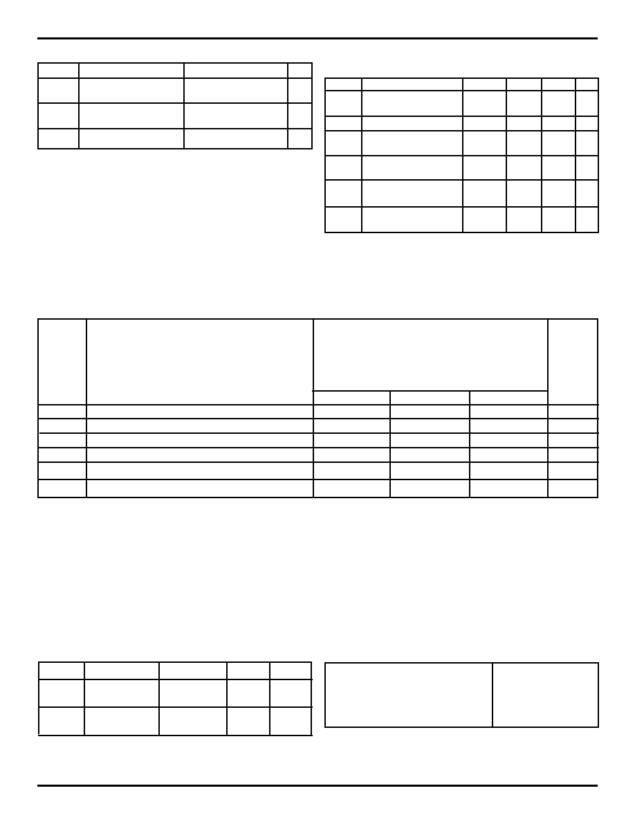
RECOMMENDED DC
OPERATING CONDITIONS
Symbol
Parameter
Min.
Typ.
Max. Unit
V
CC
Supply Voltage
4.5
5.0
5.5
V
Com'l/Ind'l
GND
Supply Voltage
0
0
0
V
V
IH
Input High Voltage
2.0
--
--
V
Com'l/Ind'l
V
IL
(1)
Input Low Voltage
--
--
0.8
V
Com'l/Ind'l
T
A
Operating Temperature
0
--
70
∞
C
Commercial
T
A
Operating Temperature
≠40
--
85
∞
C
Industrial
NOTE:
2766 tbl 02
1. Stresses greater than those listed under ABSOLUTE MAXIMUM RAT-
INGS may cause permanent damage to the device. This is a stress rating
only and functional operation of the device at these or any other conditions
above those indicated in the operational sections of this specification is not
implied. Exposure to absolute maximum rating conditions for extended
periods may affect reliability.
ABSOLUTE MAXIMUM RATINGS
Symbol
Rating
Com'l & Ind'l
Unit
V
TERM
Terminal Voltage
≠0.5 to +7.0
V
with respect to GND
T
STG
Storage
≠55 to +125
∞
C
Temperature
I
OUT
DC Output Current
≠50 to +50
mA
Symbol
Parameter
(1)
Conditions
Max.
Unit
C
IN
(2)
Input
V
IN
= 0V
10
pF
Capacitance
C
OUT
(1,2)
Output
V
OUT
= 0V
10
pF
Capacitance
CAPACITANCE
(T
A
= +25
∞
C, f = 1.0MHz)
NOTES:
2766 tbl 05
1. With output deselected, (
OE
V
IH
).
2. Characterized values, not currently tested.
AC TEST CONDITIONS
Input Pulse Levels
GND to 3.0V
Input Rise/Fall Times
3ns
Input Timing Reference Levels
1.5V
Output Reference Levels
1.5V
Output Load
See Figure 1
2766 tbl 06
NOTE:
2766 tbl 03
1. 1.5V undershoots are allowed for 10ns once per cycle.
IDT72205LB
IDT72215LB
IDT72225LB
IDT72235LB
IDT72245LB
Commercial and Industrial
(1)
t
CLK
= 10, 15, 25 ns
Symbol
Parameter
Min.
Typ.
Max.
Unit
I
LI
(2)
Input Leakage Current (any input)
≠1
--
1
µ
A
I
LO
(3)
Output Leakage Current
≠10
--
10
µ
A
V
OH
Output Logic "1" Voltage, I
OH
= ≠2 mA
2.4
--
--
V
V
OL
Output Logic "0" Voltage, I
OL
= 8 mA
--
--
0.4
V
I
CC1
(4,5,6)
Active Power Supply Current
--
--
60
mA
I
CC2
(4,7)
Standby Current
--
--
5
mA
DC ELECTRICAL CHARACTERISTICS
(Commercial: V
CC
= 5V
±
10%, T
A
= 0
∞
C to +70
∞
C; Industrial: V
CC
= 5V
±
10%, T
A
= ≠40
∞
C to +85
∞
C )
NOTES:
1. Industrial temperature range product for the 15ns and the 25 ns speed grade is available as a standard device.
2. Measurements with 0.4
V
IN
V
CC
.
3.
OE
V
IH,
0.4
V
OUT
V
CC
.
4. Tested with outputs open (I
OUT
= 0).
5. RCLK and WCLK toggle at 20 MHZ and data inputs switch at 10 MHz.
6. For the 72205/72215/72225 the typical I
CC1
= 1.81 + 1.12*f
S
+ 0.02*C
L
*f
S
(in mA);
for the 72235/72245 the typical I
CC1
= 2.85 + 1.30*f
S
+ 0.02*C
L
*f
S
(in mA).
These equations are valid under the following conditions:
V
CC
= 5V, T
A
= 25
∞
C, f
S
= WCLK frequency = RCLK frequency (in MHz, using TTL levels), data switching at f
S
/2, C
L
= capacitive load (in pF).
7. All Inputs = V
CC
- 0.2V or GND + 0.2V, except RCLK and WCLK, which toggle at 20 MHz.
2766 tbl 04
5
IDT72205LB/72215LB/72225LB/72235LB/72245LB CMOS SyncFIFOTM
256 x 18-BIT, 512 x 18, 1,024 x 18, 2,048 x 18 and 4,096 x 18
Commercial And Industrial Temperature Ranges
NOTES:
1. Industrial temperature range is available as standard product for the 15ns
and the 25ns speed grade.
2. Pulse widths less than minimum values are not allowed.
3. Values guaranteed by design, not currently tested.
2766 tbl 07
AC ELECTRICAL CHARACTERISTICS
(Commercial: V
CC
= 5V
±
10%, T
A
= 0
∞
C to +70
∞
C; Industrial: V
CC
= 5V
±
10%, T
A
= ≠40
∞
C to +85
∞
C)
Commercial
Com'l & Ind'l
(1)
72205LB10
72205LB15
72205LB25
72215LB10
72215LB15
72215LB25
72225LB10
72225LB15
72225LB25
72235LB10
72235LB15
72235LB25
72245LB10
72245LB15
72245LB25
Symbol
Parameter
Min.
Max.
Min.
Max.
Min.
Max.
Unit
f
S
Clock Cycle Frequency
--
100
--
66.7
--
40
MHz
t
A
Data Access Time
2
6.5
2
10
2
15
ns
t
CLK
Clock Cycle Time
10
--
15
--
25
--
ns
t
CLKH
Clock HIGH Time
4.5
--
6
--
10
--
ns
t
CLKL
Clock LOW Time
4.5
--
6
--
10
--
ns
t
DS
Data Set-up Time
3
--
4
--
6
--
ns
t
DH
Data Hold Time
0
--
1
--
1
--
ns
t
ENS
Enable Set-up Time
3
--
4
--
6
--
ns
t
ENH
Enable Hold Time
0
--
1
--
1
--
ns
t
RS
Reset Pulse Width
(2)
10
--
15
--
25
--
ns
t
RSS
Reset Set-up Time
8
--
10
--
15
--
ns
t
RSR
Reset Recovery Time
8
--
10
--
15
--
ns
t
RSF
Reset to Flag and Output Time
--
15
--
20
--
25
ns
t
OLZ
Output Enable to Output in Low-Z
(3)
0
--
0
--
0
--
ns
t
OE
Output Enable to Output Valid
3
6
3
8
3
12
ns
t
OHZ
Output Enable to Output in High-Z
(3)
3
6
3
8
3
12
ns
t
WFF
Write Clock to Full Flag
--
6.5
--
10
--
15
ns
t
REF
Read Clock to Empty Flag
--
6.5
--
10
--
15
ns
t
PAF
Clock to Programmable Almost-Full
--
17
--
24
--
26
ns
Flag
t
PAE
Clock to Programmable Almost-Empty
--
17
--
24
--
26
ns
Flag
t
HF
Clock to Half-Full Flag
--
17
--
24
--
26
ns
t
XO
Clock to Expansion Out
--
6.5
--
10
--
15
ns
t
XI
Expansion In Pulse Width
3
--
6.5
--
10
--
ns
t
XIS
Expansion In Set-Up Time
3.5
--
5
--
10
--
ns
t
SKEW1
Skew time between Read Clock &
5
--
6
--
10
--
ns
Write Clock for Full Flag
t
SKEW2
Skew time between Read Clock &
5
--
6
--
10
--
ns
Write Clock for Empty Flag
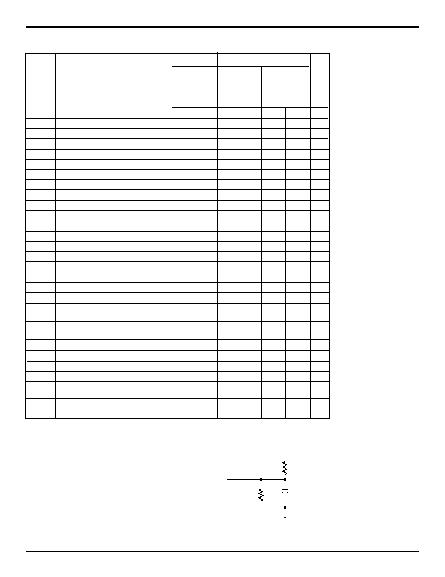
Figure 1. Output Load
* Includes jig and scope capacitances.
30pF*
1.1K
5V
680
D.U.T.
2766 drw 04