 | –≠–ª–µ–∫—Ç—Ä–æ–Ω–Ω—ã–π –∫–æ–º–ø–æ–Ω–µ–Ω—Ç: 723613 | –°–∫–∞—á–∞—Ç—å:  PDF PDF  ZIP ZIP |
CMOS CLOCKED FIFO WITH
BUS-MATCHING AND
BYTE SWAPPING 64 x 36
2002 Integrated Device Technology, Inc. All rights reserved. Product specifications subject to change without notice.
DSC-3145/1
IDT723613
MARCH 2002
IDT and the IDT logo are registered trademarks of Integrated Device Technology Inc. SyncFIFO
is a trademark of Integrated Device Technology, Inc.
COMMERCIAL AND INDUSTRIAL TEMPERATURE RANGES
1
©
FEATURES:
∑
∑
∑
∑
∑
Free-running CLKA and CLKB may be asynchronous or
coincident (permits simultaneous reading and writing of data on
a single clock edge)
∑
∑
∑
∑
∑
64 x 36 storage capacity FIFO buffering data from Port A to
Port B
∑
∑
∑
∑
∑
Mailbox bypass registers in each direction
∑
∑
∑
∑
∑
Dynamic Port B bus sizing of 36 bits (long word), 18-bits (word),
and 9 bits (byte)
∑
∑
∑
∑
∑
Selection of Big- or Little-Endian format for word and byte bus
sizes
∑
∑
∑
∑
∑
Three modes of byte-order swapping on Port B
∑
∑
∑
∑
∑
Programmable Almost-Full and Almost-Empty flags
∑
∑
∑
∑
∑
Microprocessor interface control logic
∑
∑
∑
∑
∑
FF, AF flags synchronized by CLKA
∑
∑
∑
∑
∑
EF, AE flags synchronized by CLKB
∑
∑
∑
∑
∑
Passive parity checking on each Port
∑
∑
∑
∑
∑
Parity Generation can be selected for each Port
∑
∑
∑
∑
∑
Supports clock frequencies up to 67 MHz
∑
∑
∑
∑
∑
Fast access times of 10 ns
∑
∑
∑
∑
∑
Available in 132-pin quad flatpack (PQFP) or space-saving
120-pin thin quad flatpack (TQFP)
∑
∑
∑
∑
∑
Industrial temperature range (≠40
∞∞
∞∞
∞
C to +85
∞∞
∞∞
∞
C) is available
DESCRIPTION:
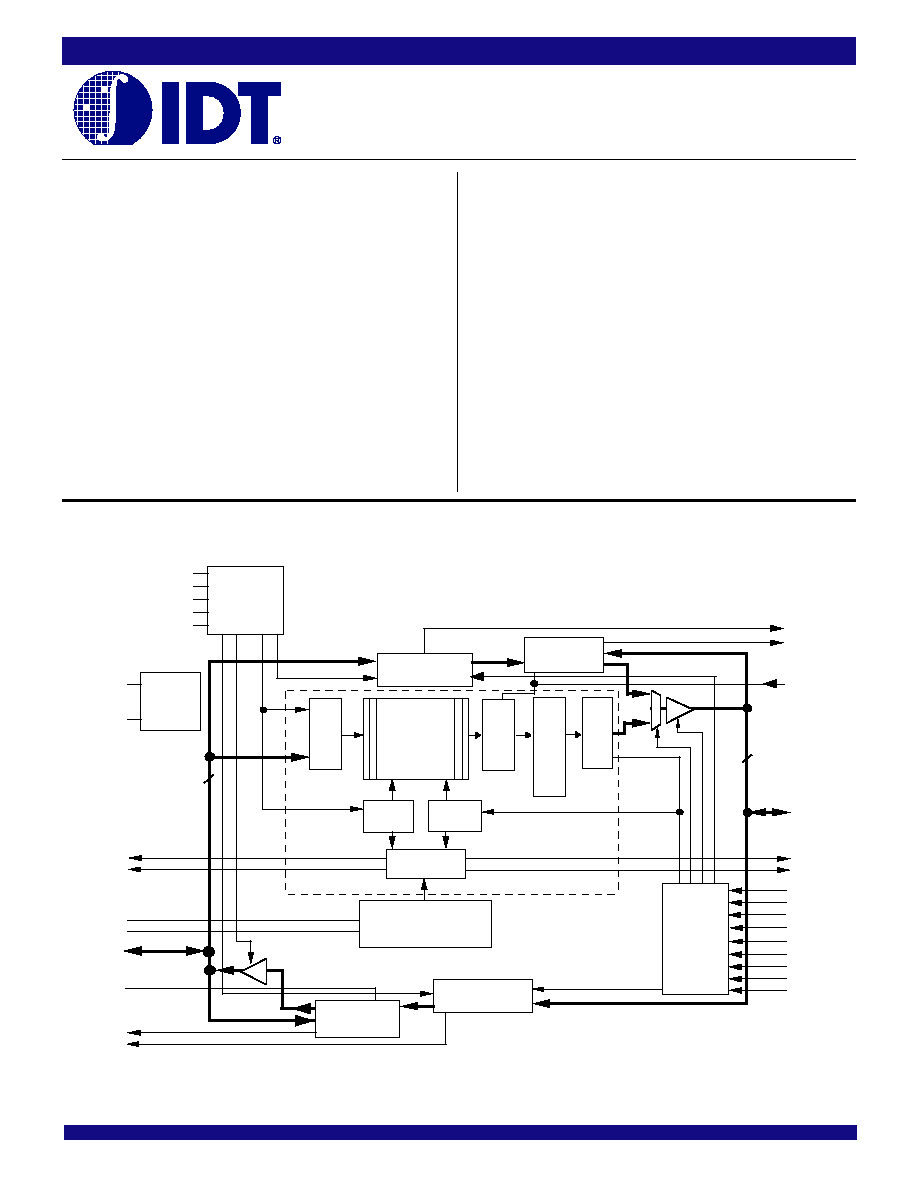
The IDT723613 is a monolithic, high-speed, low-power, CMOS synchro-
nous (clocked) FIFO memory which supports clock frequencies up to 67 MHz
and has read-access times as fast as 10 ns. The 64 x 36 dual-port SRAM FIFO
buffers data from port A to port B. The FIFO has flags to indicate empty and full
conditions, and two programmable flags, Almost-Full (
AF) and Almost-Empty
(
AE), to indicate when a selected number of words is stored in memory. FIFO
data on port B can be output in 36-bit, 18-bit, and 9-bit formats with a choice of
big- or Little-Endian configurations. Three modes of byte-order swapping are
possible with any bus-size selection. Communication between each port can
bypass the FIFO via two 36-bit mailbox registers. Each mailbox register has
a flag to signal when new mail has been stored. Parity is checked passively
FUNCTIONAL BLOCK DIAGRAM
Mail 2
Register
Mail 1
Register
Input
Register
Output
Register
64 x 36
Write
Pointer
Read
Pointer
Status Flag
Logic
CLKA
CSA
W/
R
A
ENA
MBA
Port-A
Control
Logic
Device
Control
RST
PEFA
MBF2
Port-B
Control
Logic
MBF1
EF
AE
36
B
0
- B
35
FF
AF
FS
0
FS
1
3145 drw01
Programmable
Flag Offset
Registers
A
0
- A
35
Parity
Gen/Check
Parity
Generation
FIFO
ODD/
EVEN
PGA
Parity
Gen/Check
PGB
PEFB
36
RAM ARRAY
64 x 36
Bus-Matching and
Byte Swapping
Output
Register
CLKB
CSB
W/
R
B
ENB
BE
SIZ0
SIZ1
SW0
SW1
Port-B
Control
Logic
2
COMMERCIAL AND INDUSTRIAL
TEMPERATURE RANGES
IDT723613 CMOS CLOCKED FIFO WITH
BUS-MATCHING AND BYTE SWAPPING 64 x 36
DESCRIPTION (CONTINUED)
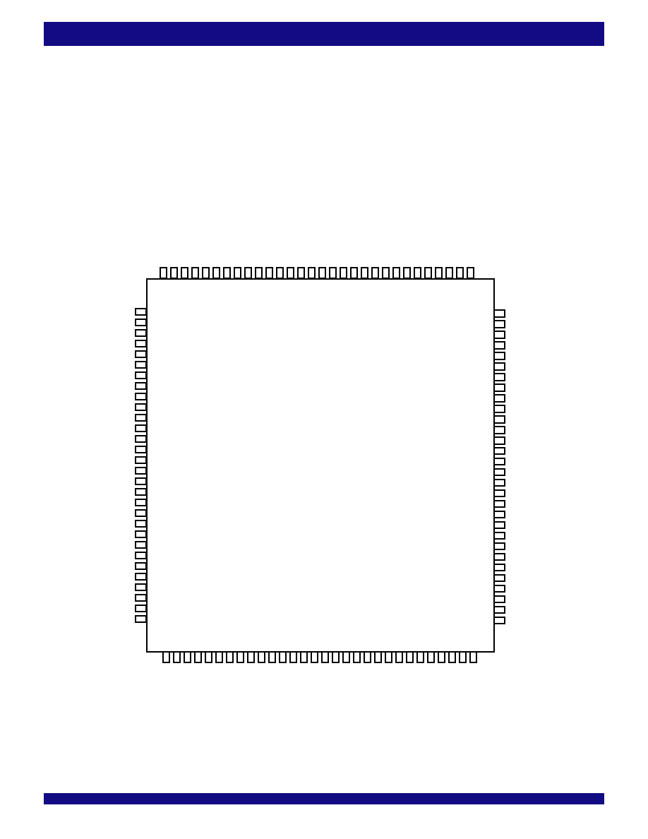
PIN CONFIGURATIONS
another and can be asynchronous or coincident. The enables for each port are
arranged to provide a simple interface between microprocessors and/or buses
with synchronous interfaces.
The Full Flag (
FF) and Almost-Full (AF) flag of the FIFO are two-stage
synchronized to the port clock (CLKA) that writes data into its array. The Empty
Flag (
EF) and Almost-Empty (AE) flag of the FIFO are two-stage synchronized
to the port clock (CLKB) that reads data from its array.
The IDT723613 is characterized for operation from 0∞C to 70∞C.
on each port and may be ignored if not desired. Parity generation can be
selected for data read from each port. Two or more devices may be used in
parallel to create wider data paths.
The IDT723613 is a synchronous (clocked) FIFO, meaning each port
employs a synchronous interface. All data transfers through a port are gated
to the LOW-to-HIGH transition of a continuous (free-running) port clock by
enable signals. The continuous clocks for each port are independent of one
NOTE:
1. NC = No internal connection.
TQFP (PN120-1, ORDER CODE: PF)
TOP VIEW
3145 drw02
A
23
A
22
A
21
GND
A
20
A
19
A
18
A
17
A
16
A
15
A
14
A
13
A
12
A
11
A
10
GND
A
9
A
8
A
7
V
CC
A
6
A
5
A
4
A
3
GND
A
2
A
1
A
0
NC
NC
1
2
3
4
5
6
7
8
9
10
11
12
13
14
15
16
17
18
19
20
21
22
23
24
25
26
27
28
29
30
B
22
B
21
GND
B
20
B
19
B
18
B
17
B
16
B
15
B
14
B
13
B
12
B
11
B
10
GND
B
9
B
8
B
7
V
CC
B
6
B
5
B
4
B
3
GND
B
2
B
1
B
0
EF
AE
NC
90
89
88
87
86
85
84
83
82
81
80
79
78
77
76
75
74
73
72
71
70
69
68
67
66
65
64
63
62
61
AF FF
CSA
ENA
CLKA
W/
R
A
V
CC
PGA
PEFA MBF2
MBA
FS
1
FS
0
ODD/
EVEN
RST
GND
BE
SW1
SW0
SIZ1
MBF1
SIZ0
PEFB
PGB
V
CC
W/
R
B
CLKB
ENB
CSB
NC
31
32
33 34
35
36 37
38
39
40
41
42
43
44
45
46
47
48 49
50 51
52
53
54
55
56
57
58
59
60
91
120
119
118
117
116
115
114
113
112
111
110
109
108
107
106
105
104
103
102
101
100
99
98
97
96
95
94
93
92
B
23
A
24
A
25
A
26
V
CC
A
27
A
28
A
29
GND
A
30
A
31
A
34
A
35
B
35
GND
B
34
B
33
B
32
B
30
B
31
GND
B
29
B
28
B
27
V
CC
B
26
B
25
B
24
A
32
A
33

3
COMMERCIAL AND INDUSTRIAL
TEMPERATURE RANGES
IDT723613 CMOS CLOCKED FIFO WITH
BUS-MATCHING AND BYTE SWAPPING 64 x 36
GND
AE
EF
B
0
B
1
B
2
GND
B
3
B
4
B
5
B
6
V
CC
B
7
B
8
B
9
GND
B
10
B
11
V
CC
B
12
B
13
B
14
GND
B
15
B
16
B
17
B
18
B
19
B
20
GND
B
21
B
22
B
23
GND
NC
NC
A
0
A
1
A
2
GND
A
3
A
4
A
5
A
6
V
CC
A
7
A
8
A
9
GND
A
10
A
11
V
CC
A
12
A
13
A
14
GND
A
15
A
16
A
17
A
18
A
19
A
20
GND
A
21
A
22
A
23
18
19
20
21
22
23
24
25
26
27
28
29
30
31
32
33
34
35
36
37
38
39
40
41
42
43
44
45
46
47
48
49
50
116
115
114
113
112
111
110
109
108
107
106
105
104
103
102
101
100
99
98
97
96
95
94
93
92
91
90
89
88
87
86
85
84
3145 drw03
117
17
16
15
14
13
12
11
10
9
8
7
6
5
4
3
2
1
132
131
130
129
128
127
126
125
124
123
122
121
120
119
118
V
CC
V
CC
A
24
A
25
A
26
A
27
GND
A
28
A
29
V
CC
A
30
A
31
A
32
GND
A
33
A
34
A
35
GND
B
35
B
34
B
33
GND
B
32
B
31
B
30
V
CC
B
29
B
28
B
27
GND
B
26
B
25
B
24
51
52
53
54
55
56
57
58
59
60
61
62
63
64
65
66
67
68
69
70
71
72
73
74
75
76
77
78
79
80
81
82
83
NC
AF FF CSA
ENA
CLKA
W/
R
A
V
CC
PGA
FS
0
ODD/
EVEN
FS
1
PEFA
MBF2
RST
BE
GND
SW1
SW0
SIZ1
MBF1
GND
PEFB
V
CC
W/
R
B
CLKB
ENB
CSB
NC
GND
MBA
SIZ0
PGB
*
NOTES:
1. NC = No internal connection.
2. Uses Yamaichi socket IC51-1324-828.
PQFP
(2)
(PQ132-1, ORDER CODE: PQF)
TOP VIEW
* Electrical pin 1 in center of beveled edge. Pin 1 identifier in corner.
PIN CONFIGURATIONS (CONTINUED)

4
COMMERCIAL AND INDUSTRIAL
TEMPERATURE RANGES
IDT723613 CMOS CLOCKED FIFO WITH
BUS-MATCHING AND BYTE SWAPPING 64 x 36
Symbol
Name
I/O
Description
A
0
-A
35
Port A Data
I/O
36-bit bidirectional data port for side A.
AE
Almost-Empty Flag
O
Programmable Almost-Empty flag synchronized to CLKB. It is LOW when Port B the number of 36-bit
Port B
words in the FIFO is less than or equal to the value in the offset register, X.
AF
Almost-Full Flag
O
Programmable Almost-Full flag synchronized to CLKA. It is LOW when the number of 36-bit empty location
Port A
in the FIFO is less than or equal to the value in the offset register, X.
B
0
-B
35
Port B Data
I/O
36-bit bidirectional data port for side B
B E
Big-Endian Select
I
Selects the bytes on port B used during byte or word FIFO reads. A LOW on
BE selects the most significant
bytes on B
0
-B
35
for use, and a HIGH selects the least significant bytes.
CLKA
Port A Clock
I
CLKA is a continuous clock that synchronizes all data transfers through port A and can be asynchronous or
coincident to CLKB.
FF and AF are synchronized to the LOW-to-HIGH transition of CLKA.
CLKB
Port B Clock
I
CLKB is a continuous clock that synchronizes all data transfers through port B and can be asynchronous or
coincident to CLKA. Port-B byte swapping and data port sizing operations are also synchronous to the
LOW-to-HIGH transition of CLKB.
EF and AE are synchronized to the LOW-to-HIGH transition of CLKB.
CSA
Port A Chip Select
I
CSA must be LOW to enable a LOW-to-HIGH transition of CLKA to read or write data on port A. The
A
0
-A
35
outputs are in the high-impedance state when
CSA is HIGH.
CSB
Port B Chip Select
I
CSB must be LOW to enable a LOW-to-HIGH transition of CLKB to read or write data on port B. The
B
0
-B
35
outputs are in the high-impedance state when
CSB is HIGH.
EF
Empty Flag
O
EF is synchronized to the LOW-to-HIGH transition of CLKB. When EF is LOW, the FIFO is empty, and
Port B
reads from its memory are disabled. Data can be read from the FIFO to its output register when
EF is
HIGH.
EF is forced LOW when the device is reset and is set HIGH by the second LOW-to-HIGH transition
of CLKB after data is loaded into empty FIFO memory.
ENA
Port A Enable
I
ENA must be HIGH to enable a LOW-to-HIGH transition of CLKA to read or write data on port A.
ENB
Port B Enable
I
ENB must be HIGH to enable a LOW-to-HIGH transition of CLKB to read or write data on port B.
FF
Full Flag
O
FF is synchronized to the LOW-to-HIGH transition of CLKA. When FF is LOW, the FIFO is full, and writes
Port A
to its memory are disabled.
FF is forced LOW when the device is reset and is set HIGH by the second
LOW-to-HIGH transition of CLKA after reset.
FS
1
, FS
0
Flag Offset Selects
I
The LOW-to-HIGH transition of
RST latches the values of FS
0
and FS
1
, which loads one of four preset
values into the Almost-Full flag and Almost-Empty flag offsets.
MBA
Port A Mailbox Select
I
A high level on MBA chooses a mailbox register for a port A read or write operation. When the A0-A35
outputs are active, mail2 register data is output.
MBF1
Mail1 Register Flag
O
MBF1 is set LOW by a LOW-to-HIGH transition of CLKA that writes data to the mail1 register. Writes to the
mail1 register are inhibited while
MBF1 is set LOW. MBF1 is set HIGH by a LOW-to-HIGH transition of
CLKB when a port B read is selected and both SIZ1 and SIZ0 are HIGH.
MBF1 is set HIGH when the
device is reset.
MBF2
Mail2 Register Flag
O
MBF2 is set LOW by a LOW-to-HIGH transition of CLKB that writes data to the mail2 register. Writes to
the mail2 register are inhibited while
MBF2 is set LOW. MBF2 is set HIGH by a LOW-to-HIGH transition
of CLKA when a port A read is selected and MBA is HIGH.
MBF2 is set HIGH when the device is reset.
ODD/
Odd/Even Parity Select
I
Odd parity is checked on each port when ODD/
EVEN is HIGH, and even parity is checked when ODD
EVEN
EVEN is LOW. ODD/EVEN also selects the type of parity generated for each port if parity generation is
enabled for a read operation.
PEFA
Port A Parity Error Flag
O
When any byte applied to terminals A
0
-A
35
fails parity,
PEFA is LOW. Bytes are organized as A
0
-A
8
, A
9
-A
17
,
(Port A)
A
18
-A
26
, and A
27
-A
35
, with the most significant bit of each byte serving as the parity bit. The type of parity
checked is determined by the state of the ODD/
EVEN input. The parity trees used to check the A
0
-A
35
inputs are shared by the mail2 register to generate parity if parity generation is selected by PGA. Therefore,
if a mail2 read with parity generation is set up by having
CSA LOW, ENA HIGH, W/RA LOW, MBA HIGH
and PGA HIGH, the
PEFA flag is forced HIGH regardless of the state of the A
0
-A
35
inputs.
PEFB
Port B Parity Error Flag
O
When any valid byte applied to terminals B
0
-B
35
fails parity,
PEFB is LOW. Bytes are organized as B
0
-B
8
,
(PortB)
B
9
-B
17
, B18-B26, and B
27
-B
35
, with the most significant bit of each byte serving as the parity bit. A byte is
valid when it is used by the bus size selected for port B. The type of parity checked is determined by the
state of the ODD/
EVEN input. The parity trees used to check the B
0
-B
35
inputs are shared by the mail1
register to generate parity if parity generation is selected by PGB. Therefore, if a mail1 read with parity
generation is set up by having
CSB LOW, ENB HIGH, W/RB LOW, SIZ1 and SIZ0 HIGH and PGB
HIGH, the
PEFB flag is forced HIGH regardless of the state of the B
0
-B
35
inputs.
PIN DESCRIPTION
5
COMMERCIAL AND INDUSTRIAL
TEMPERATURE RANGES
IDT723613 CMOS CLOCKED FIFO WITH
BUS-MATCHING AND BYTE SWAPPING 64 x 36
Symbol
Name
I/O
Description
PGA
Port A Parity Generation
I
Parity is generated for data reads from the mail2 register when PGA is HIGH. The type of parity
generated is selected by the state of the ODD/
EVEN input. Bytes are organized at A
0
-A
8
, A
9
-A
17
,
A
18
-A
26
, and A
27
-A
35
. The generated parity bits are output in the most significant bit of each byte.
PGB
Port B Parity
I
Parity is generated for data reads from port B when PGB is HIGH. The type of parity generated is
selected by the state of the ODD/
EVEN input. Bytes are organized as B
0
-B
8
, B
9
-B
17
, B
18
-B
26
, and
B
27
-B
35
. The generated parity bits are output in the most significant bit of each byte.
RST
Reset
I
To reset the device, four LOW-to-HIGH transitions of CLKA and four LOW-to-HIGH transitions of CLKB
must occur while
RST is LOW. This sets the AF, MBF1, and MBF2 flags HIGH and the EF, AE, and FF
flags LOW. The LOW-to-HIGH transition of
RST latches the status of the FS
1
and FS
0
inputs to select
Almost-Full flag and Almost-Empty flag offset.
SIZ0,
Port B Bus Size Selects
I
A LOW-to-HIGH transition of CLKB latches the states of SIZ0, SIZ1, and
BE, and the following LOW-to
SIZ1
(Port B)
HIGH transition of CLKB implements the latched states as a port B bus size. Port B bus sizes can be
long word, word, or byte. A HIGH on both SIZ0 and SIZ1 accesses the mailbox registers for a port B 36-bit
write or read.
SW0,
Port B Byte Swap Selects
I
At the beginning of each long word FIFO read, one of four modes of byte-order swapping is selected by
SW1
(Port B)
SW0 and SW1. The four modes are no swap, byte swap, word swap, and byte-word swap. Byte order
swapping is possible with any bus-size selection.
W/
RA
Port A Write/Read Select
I
A HIGH selects a write operation and a LOW selects a read operation on port A for a LOW-to-HIGH
Select
transition of CLKA. The A
0
-A
35
outputs are in the high-impedance state when W/
RA is HIGH.
W/
RB
Port B Write/Read Select
I
A HIGH selects a write operation and a LOW selects a read operation on port B for a LOW-to-HIGH
transition of CLKB. The B
0
-B
35
outputs are in the high-impedance state when W/
RB is HIGH.
PIN DESCRIPTION (CONTINUED)