 | –≠–ª–µ–∫—Ç—Ä–æ–Ω–Ω—ã–π –∫–æ–º–ø–æ–Ω–µ–Ω—Ç: 723622 | –°–∫–∞—á–∞—Ç—å:  PDF PDF  ZIP ZIP |
1
2001 Integrated Device Technology, Inc. All rights reserved. Product specifications subject to change without notice.
DSC-3022/3
DECEMBER 2001
CMOS SyncBiFIFO
TM
256 x 36 x 2, 512 x 36 x 2,
1,024 x 36 x 2
IDT723622
IDT723632
IDT723642
IDT, the IDT logo are registered trademarks of Integrated Device Technology, Inc. SyncBiFIFO is a trademark of Integrated Device Technology, Inc.
COMMERCIAL TEMPERATURE RANGE
.EATURES:
∑
∑
∑
∑
∑
Memory storage capacity:
IDT723622
≠
256 x 36 x 2
IDT723632
≠
512 x 36 x 2
IDT723642
≠
1,024 x 36 x 2
∑
∑
∑
∑
∑
Free-running CLKA and CLKB may be asynchronous or
coincident (simultaneous reading and writing of data on a single
clock edge is permitted)
∑
∑
∑
∑
∑
Two independent clocked FIFOs buffering data in opposite
directions
∑
∑
∑
∑
∑
Mailbox bypass register for each FIFO
∑
∑
∑
∑
∑
Programmable Almost-Full and Almost-Empty flags
∑
∑
∑
∑
∑
Microprocessor Interface Control Logic
∑
∑
∑
∑
∑
IRA, ORA,
AEA, and AFA flags synchronized by CLKA
∑
∑
∑
∑
∑
IRB, ORB,
AEB, and AFB flags synchronized by CLKB
∑
∑
∑
∑
∑
Supports clock frequencies up to 83MHz
∑
∑
∑
∑
∑
Fast access times of 8ns
∑
∑
∑
∑
∑
Available in 132-pin Plastic Quad Flatpack (PQFP) or space-
saving 120-pin Thin Quad Flatpack (TQFP)
∑
∑
∑
∑
∑
Low-power 0.8-Micron Advanced CMOS technology
∑
∑
∑
∑
∑
Industrial temperature range (≠40
∞∞
∞∞
∞
C to +85
∞∞
∞∞
∞
C) is available
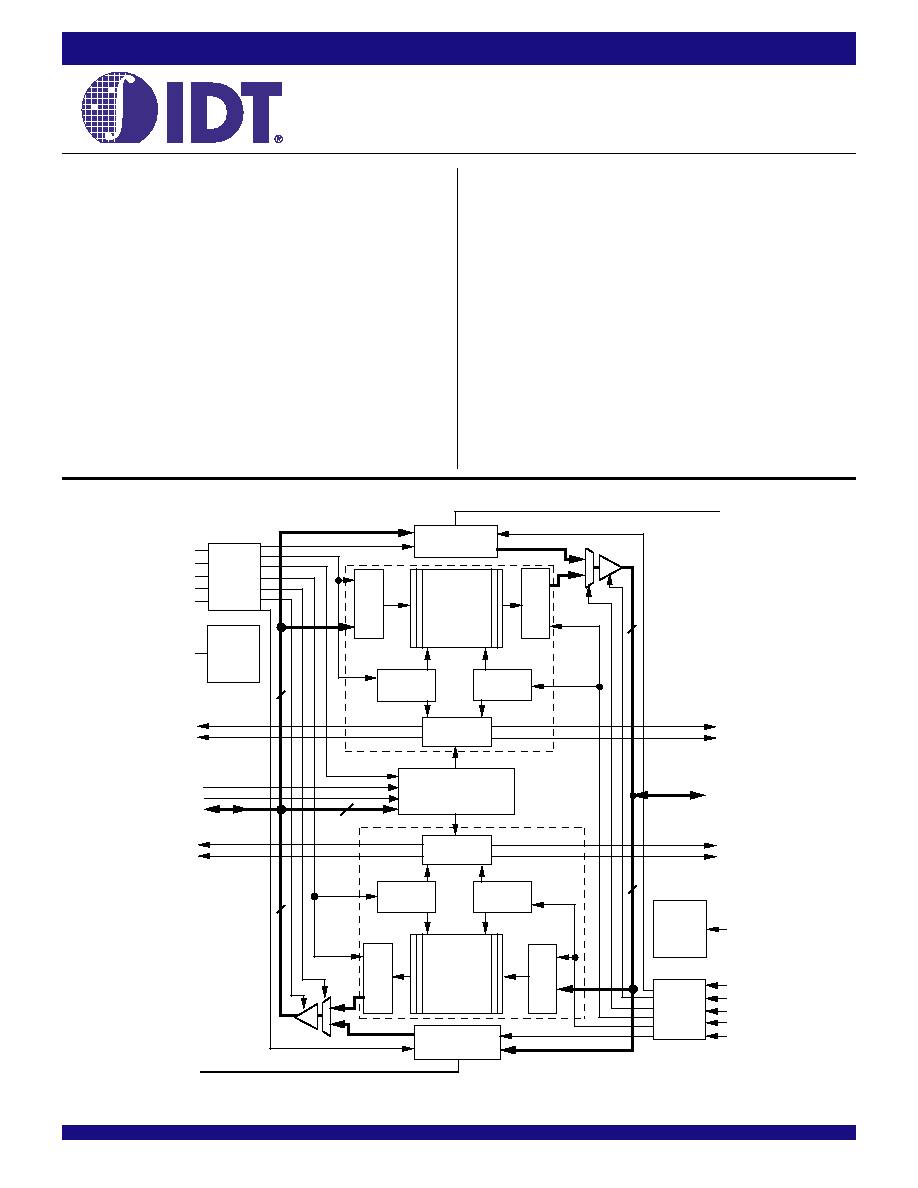
DESCRIPTION:
The IDT723622/723632/723642 are a monolithic, high-speed, low-power,
CMOS Bidirectional SyncFIFO (clocked) memory which supports clock fre-
quencies up to 83MHz and have read access times as fast as 8ns. Two
independent 256/512/1,024 x 36 dual-port SRAM FIFOs on board each chip
buffer data in opposite directions. Communication between each port may
bypass the FIFOs via two 36-bit mailbox registers. Each mailbox register has
a flag to signal when new mail has been stored.
These devices are a synchronous (clocked) FIFO, meaning each port
employs a synchronous interface. All data transfers through a port are gated
to the LOW-to-HIGH transition of a port clock by enable signals. The clocks for
each port are independent of one another and can be asynchronous or
Mail 1
Register
Programmable Flag
Offset Registers
Input
Register
Output
Register
RAM
ARRAY
256 x 36
512 x 36
1,024 x 36
Write
Pointer
Read
Pointer
Status Flag
Logic
Input
Register
Output
Register
RAM
ARRAY
256 x 36
512 x 36
1,024 x 36
Write
Pointer
Read
Pointer
Status Flag
Logic
CLKA
CSA
W/
R
A
ENA
MBA
Port-A
Control
Logic
FIFO1,
Mail1
Reset
Logic
RST1
Mail 2
Register
MBF2
CLKB
CSB
W
/RB
ENB
MBB
Port-B
Control
Logic
FIFO2,
Mail2
Reset
Logic
RST2
MBF1
FIFO 1
FIFO 2
10
ORB
AEB
36
36
IRB
AFB
B
0
- B
35
IRA
AFA
FS
0
FS
1
A
0
- A
35
ORA
AEA
3022 drw 01
36
36
.UNCTIONAL BLOCK DIAGRAM
2
IDT723622/723632/723642 CMOS SyncBiFIFOTM
256 x 36 x 2, 512 x 36 x 2, 1,024 x 36 x 2
COMMERCIAL TEMPERATURE RANGE
DESCRIPTION (CONTINUED)
NOTES:
1. NC ≠ no internal connection
2. Uses Yamaichi socket IC51-1324-828
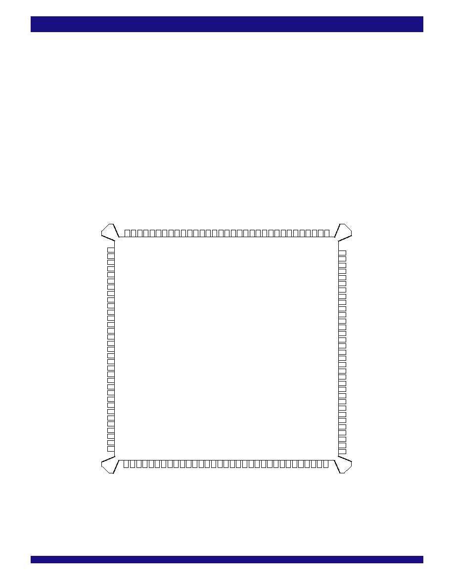
PIN CON.IGURATION
PQFP (PQ132-1, order code: PQF)
TOP VIEW
NC
NC
A
35
A
34
A
33
A
32
V
CC
A
31
A
30
GND
A
29
A
28
A
27
A
26
A
25
A
24
A
23
GND
A
22
V
CC
A
21
A
20
A
19
A
18
GND
A
17
A
16
A
15
A
14
A
13
V
CC
A
12
NC
NC
B
35
B
34
B
33
B
32
GND
B
31
B
30
B
29
B
28
B
27
B
26
V
CC
B
25
B
24
GND
B
23
B
22
B
21
B
20
B
19
B
18
GND
B
17
B
16
V
CC
B
15
B
14
B
13
B
12
GND
NC
NC
18
19
20
21
22
23
24
25
26
27
28
29
30
31
32
33
34
35
36
37
38
39
40
41
42
43
44
45
46
47
48
49
50
116
115
114
113
112
111
110
109
108
107
106
105
104
103
102
101
100
99
98
97
96
95
94
93
92
91
90
89
88
87
86
85
84
3022 drw 02
NC
NC
NC
V
CC
CLKB
ENB
W
/RB
CSB
GND
IRB
ORB
AFB AEB
V
CC
MBF1
MBB
RST2
FS1 GND
FS0
RST1
MBA
MBF2 AEA AFA
V
CC
ORA
IRA
CSA
W/
R
A
ENA CLKA GND
117
17
16
15
14
13
12
11
10
9
8
7
6
5
4
3
2
1
132
131
130
129
128
127
126
125
124
123
122
121
120
119
118
NC
NC
B
11
B
10
B
9
B
7
B
8
V
CC
B
6
GND
B
5
B
4
B
3
B
2
B
1
B
0
GND
A
0
A
1
A
2
V
CC
A
3
A
4
A
5
GND
A
6
A
7
A
8
A
9
A
10
A
11
GND
NC
74
76
77
78
79
80
81
82
83
75
51
52
53
54
55
56
57
58
59
60
61 62
63
64
65
66
67
68
69
70
71
72
73
coincident. The enables for each port are arranged to provide a simple
bidirectional interface between microprocessors and/or buses with synchro-
nous control.
Each FIFO has a programmable Almost-Empty flag (
AEA and AEB) and a
progammable Almost-Full flag (
AFA and AFB). AEA and AEB indicate when
a selected number of words remain in the FIFO memory.
AFA and AFB indicate
when the FIFO contains more than a selected number of words.
The Input Ready (IRA, IRB) and Almost-Full (
AFA, AFB) flags of a FIFO
are two-stage synchronized to the port clock that writes data into its array. The
Output Ready (ORA, ORB) and Almost-Empty (
AEA, AEB) flags of a FIFO are
two-stage synchronized to the port clock that reads data from its array. Offset
values for the Almost-Full and Almost-Empty flags of both FIFOs can be
programmed from Port A.
Two or more devices may be used in parallel to create wider data paths.
If, at any time, the FIFO is not actively performing a function, the chip will
automatically power down. During the power down state, supply current
consumption (I
CC
) is at a minimum. Initiating any operation (by activating control
inputs will immediately take the device out of the power down state.
The 723622/723632/723642 are characterized for operation from 0
∞
C to
70
∞
C. Industrial temperature range (-40
∞
C to +85
∞
C) is available by special
order. They are fabricated using IDT's high speed, submicron CMOS technology.
3
IDT723622/723632/723642 CMOS SyncBiFIFOTM
256 x 36 x 2, 512 x 36 x 2, 1,024 x 36 x 2
COMMERCIAL TEMPERATURE RANGE
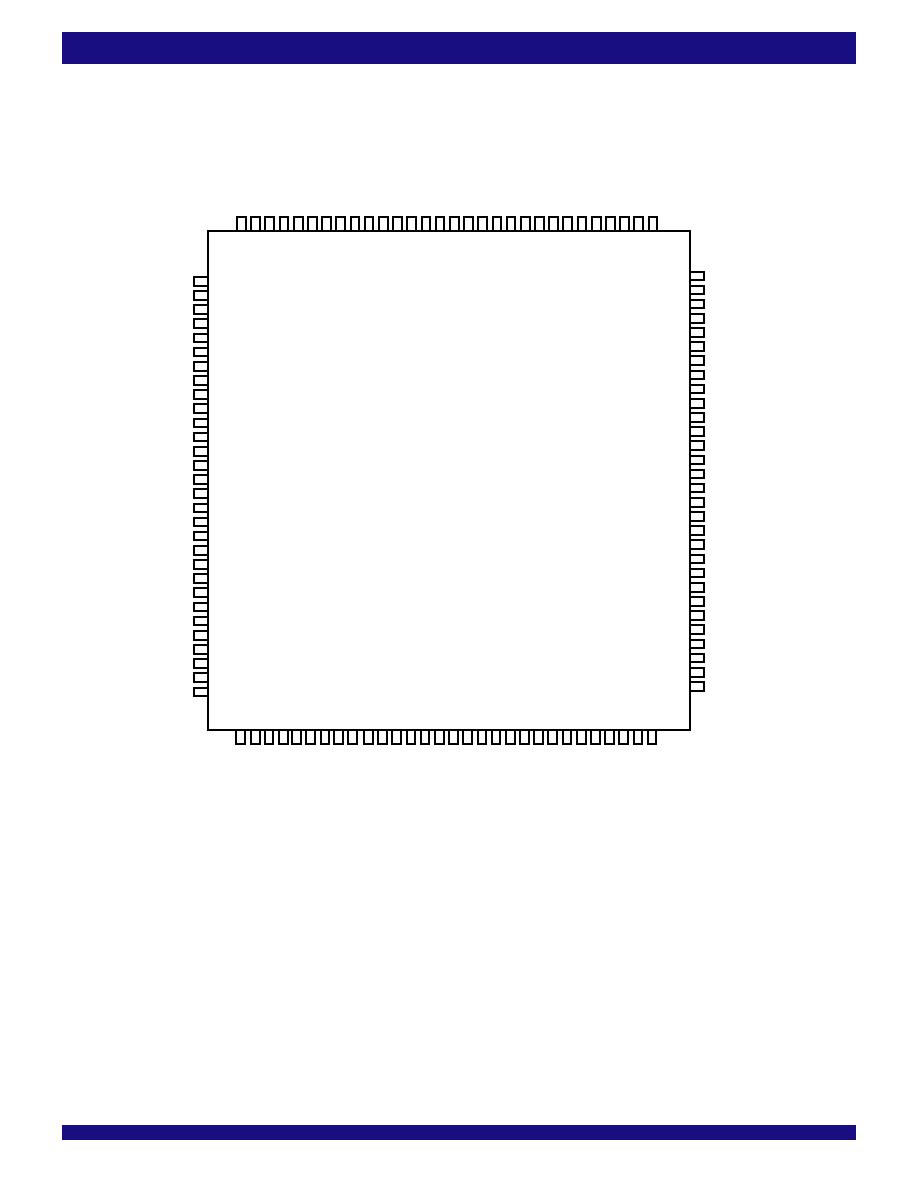
PIN CON.IGURATION (CONTINUED)
TQFP (PN120-1, order code: PF)
TOP VIEW
3022 drw 03
A
35
A
34
A
33
A
32
V
CC
A
31
A
30
GND
A
29
A
28
A
27
A
26
A
25
A
24
A
23
GND
A
22
V
CC
A
21
A
20
A
19
A
18
GND
A
17
A
16
A
15
A
14
A
13
V
CC
A
12
1
2
3
4
5
6
7
8
9
10
11
12
13
14
15
16
17
18
19
20
21
22
23
24
25
26
27
28
29
30
B
35
B
34
B
33
B
32
GND
B
31
B
30
B
29
B
28
B
27
B
26
V
CC
B
25
B
24
GND
B
23
B
22
B
21
B
20
B
19
B
18
GND
B
17
B
16
V
CC
B
15
B
14
B
13
B
12
GND
90
89
88
87
86
85
84
83
82
81
80
79
78
77
76
75
74
73
72
71
70
69
68
67
66
65
64
63
62
61
91
120
119
118
117
116
115
114
113
112
111
110
109
108
107
106
105
104
103
102
101
100
99
98
97
96
95
94
93
92
V
CC
GND
CLKA
ENA
W/
R
A
CSA
IRA
ORA
V
CC
AFA AEA MBF2
MBA
RST1
FS0 GND
FS1
RST2
MBB
MBF1
V
CC
AEB AFB
ORB
IRB
GND
CSB W
/RB
ENB
CLKB
GND
A
11
A
10
A
9
A
8
A
7
A
6
GND
A
5
A
4
A
3
V
CC
A
2
A
1
A
0
GND
B
0
B
1
B
2
B
3
B
4
B
5
GND
B
6
V
CC
B
7
B
8
B
9
B
10
B
11
31
32
33
34 35 36
37 38
39
40
41
42
43
44
45
46
47 48
49
50
51
52
53
54 55
56
57 58
59
60
4
IDT723622/723632/723642 CMOS SyncBiFIFOTM
256 x 36 x 2, 512 x 36 x 2, 1,024 x 36 x 2
COMMERCIAL TEMPERATURE RANGE
PIN DESCRIPTIONS
Symbol
Name
I/O
Description
A0-A35
Port A Data
I/0
36-bit bidirectional data port for side A.
AEA
Port A Almost-
O
Programmable Almost-Empty flag synchronized to CLKA. It is LOW when the number of words
Empty Flag
(Port A)
in FIFO2 is less than or equal to the value in the Almost-Empty A Offset register, X2.
AEB
Port B Almost-
O
Programmable Almost-Empty flag synchronized to CLKB. It is LOW when the number of words
Empty Flag
(Port B)
in FIFO1 is less than or equal to the value in the Almost-Empty B Offset register, X1.
AFA
Port A Almost-
O
Programmable Almost-Full flag synchronized to CLKA. It is LOW when the number of empty
Full Flag
(Port A)
locations in FIFO1 is less than or equal to the value in the Almost-Full A Offset register, Y1.
AFB
Port B Almost-
O
Programmable Almost-Full flag synchronized to CLKB. It is LOW when the number of empty
Full Flag
(Port B)
locations in FIFO2 is less than or equal to the value in the Almost-Full B Offset register, Y2.
B0 - B35
Port B Data
I/O
36-bit bidirectional data port for side B.
CLKA
Port A Clock
I
CLKA is a continuous clock that synchronizes all data transfers through port A and can be
asynchronous or coincident to CLKB. IRA, ORA,
AFA, and AEA are all synchronized to the
LOW-to-HIGH transition of CLKA.
CLKB
Port B Clock
I
CLKB is a continuous clock that synchronizes all data transfers through port B and can be
asynchronous or coincident to CLKA. IRB, ORB,
AFB, and AEB are synchronized to the LOW-
to-HIGH transition of CLKB.
CSA
Port A Chip
I
CSA must be LOW to enable a LOW-to-HIGH transition of CLKA to read or write on port A.
Select
The A0-A35 outputs are in the high-impedance state when
CSA is HIGH.
CSB
Port B Chip
I
CSB must be LOW to enable a LOW-to-HIGH transition of CLKB to read or write data on
Select
port B. The B0-B35 outputs are in the high-impedance state when
CSB is HIGH.
ENA
Port A Enable
I
ENA must be HIGH to enable a LOW-to-HIGH transition of CLKA to read or write data on port A.
ENB
Port B Enable
I
ENB must be HIGH to enable a LOW-to-HIGH transition of CLKB to read or write data on port B.
FS1, FS0
Flag Offset
I
The LOW-to-HIGH transition of a FlFO's Reset input latches the values of FS0 and FS1.
Selects
If either FS0 or FS1 is HIGH when a Reset goes HIGH, one of three preset values is selected as
the offset for the FlFOs Almost-Full and Almost-Empty flags. If both FIFOs are reset simultaneously
and both FS0 and FS1 are LOW when
RST1 and RST2 go HIGH, the first four writes to FIFO1
load the Almost-Empty and Almost-Full offsets for both FlFOs.
IRA
Input Ready
O
IRA is synchronized to the LOW-to-HIGH transition of CLKA. When IRA is LOW, FIFO1 is full
Flag
(Port A)
and writes to its array are disabled. IRA is set LOW when FIFO1 is reset and is set HIGH on the
second LOW-to-HIGH transition of CLKA after reset.
IRB
Input Ready
O
IRB is synchronized to the LOW-to-HIGH transition of CLKB. When IRB is LOW, FIFO2 is full
Flag
(Port B)
and writes to its array are disabled. IRB is set LOW when FIFO2 is reset and is set HIGH on the
second LOW-to-HIGH transition of CLKB after reset.
MBA
Port A Mailbox
I
A HIGH level on MBA chooses a mailbox register for a port A read or write operation.
Select
When the A0-A35 outputs are active, a HIGH level on MBA selects data from the mail2 register for
output and a LOW level selects FIFO2 output register data for output.
MBB
Port B Mailbox
I
A HIGH level on MBB chooses a mailbox register for a port B read or write operation. When the
Select
B0-B35 outputs are active, a HIGH level on MBB selects data from the mail1 register or output and
a LOW level selects FIFO1 output register data for output.
MBF1
Mail1 Register
O
MBF1 is set LOW by a LOW-to-HIGH transition of CLKA that writes data to the mail1
Flag
register. Writes to the mail1 register are inhibited while
MBF1 is LOW. MBF1 is set HIGH by
a LOW-to-HIGH transition of CLKB when a port B read is selected and MBB is HIGH.
MBF1 is
set HIGH when FIFO1 is reset.
MBF2
Mail2 Register
O
MBF2 is set LOW by a LOW-to-HIGH transition of CLKB that writes data to the mail2 register.
Flag
Writes to the mail2 register are inhibited while
MBF2 is LOW. MBF2 is set HIGH by a LOW-
to-HIGH transition of CLKA when a port A read is selected and MBA is HIGH.
MBF2 is also
set HIGH when FIFO2 is reset.
5
IDT723622/723632/723642 CMOS SyncBiFIFOTM
256 x 36 x 2, 512 x 36 x 2, 1,024 x 36 x 2
COMMERCIAL TEMPERATURE RANGE
Symbol
Name
I/O
Description
ORA
Output Ready
O
ORA is synchronized to the LOW-to-HIGH transition of CLKA. When ORA is LOW, FIFO2 is
Flag
(Port A)
empty and reads from its memory are disabled. Ready data is present on the output register
of FIFO2 when ORA is HIGH. ORA is forced LOW when FlFO2 is reset and goes HIGH on the
third LOW-to-HIGH transition of CLKA after a word is loaded to empty memory.
ORB
Output Ready
O
ORB is synchronized to the LOW-to-HIGH transition of CLKB. When ORB is LOW, FlFO1 is
Flag
(Port B)
empty and reads from its memory are disabled. Ready data is present on the output register of FIFO1
when ORB is HIGH. ORB is forced LOW when FIFO1 is reset and goes HIGH on the third LOW-to-
HIGH transition of CLKB after a word is loaded to empty memory.
RST1
FIFO1 Reset
I
To reset FIFO1, four LOW-to-HIGH transitions of CLKA and four LOW-to-HIGH transitions of CLKB
must occur while
RST1 is LOW. The LOW-to-HIGH transition of RST1 latches the status of FS0
and FS1 for
AFA and AEB offset selection. FIFO1 must be reset upon power up before data is
written to its RAM.
RST2
FIFO2 Reset
I
To reset FIFO2, four LOW-to-HIGH transitions of CLKA and four LOW-to-HIGH transitions of CLKB
must occur while
RST2 is LOW. The LOW-to-HIGH transition of RST2 latches the status of FS0
and FS1 for
AFB and AEA offset selection. FIFO2 must be reset upon power up before data is
written to its RAM.
W/
RA
Port A Write/
I
A HIGH selects a write operation and a LOW selects a read operation on port A for a LOW-to-HIGH
Read Select
transition of CLKA. The A0-A35 outputs are in the HIGH impedance state when W/
RA is HIGH.
W/RB
Port B Write/
I
A LOW selects a write operation and a HIGH selects a read operation on port B for a LOW-to-HIGH
Read Select
transition of CLKB. The B0-B35 outputs are in the high-impedance state when
W/RB is LOW.
PIN DESCRIPTIONS (CONTINUED)