 | –≠–ª–µ–∫—Ç—Ä–æ–Ω–Ω—ã–π –∫–æ–º–ø–æ–Ω–µ–Ω—Ç: 728980 | –°–∫–∞—á–∞—Ç—å:  PDF PDF  ZIP ZIP |

1
JANUARY 2001
TIME SLOT INTERCHANGE
DIGITAL SWITCH
256 x 256
IDT728980
2001 Integrated Device Technology, Inc.
DSC-5706/1
.UNCTIONAL BLOCK DIAGRAM
Microprocessor Interface
Control Register
Timing
Unit
RX0
RX1
RX2
RX3
RX4
RX5
RX6
RX7
TX0
TX1
TX2
TX3
TX4
TX5
TX6
TX7
ODE
F0i
C4i
V
CC
CS
DS
R/
W
A0/
A5
GND
CCO
DTA
D0/
D7
5706 drw01
Data
Memory
Output MUX
Connection
Memory
Receive
Serial Data
Streams
Transmit
Serial Data
Streams
.EATURES:
∑
∑
∑
∑
∑
256 x 256 channel non-blocking switch
∑
∑
∑
∑
∑
Serial Telecom Bus Compatible (ST-BUS
Æ
)
∑
∑
∑
∑
∑
8 RX inputs--32 channels at 64 Kbit/s per serial line
∑
∑
∑
∑
∑
8 TX output--32 channels at 64 Kbit/s per serial line
∑
∑
∑
∑
∑
Three-state serial outputs
∑
∑
∑
∑
∑
Microprocessor Interface (8-bit data bus)
∑
∑
∑
∑
∑
5V Power Supply
∑
∑
∑
∑
∑
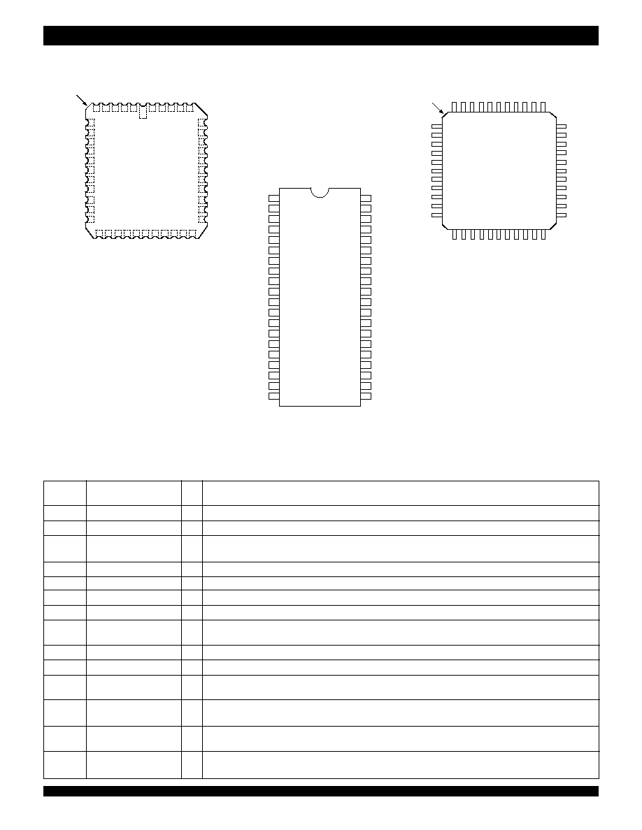
Available in 44-pin Plastic Leaded Chip Carrier (PLCC), 40-pin
Plastic Dip (P-DIP) and 44-pin Plastic Quad Flatpack (PQFP)
∑
∑
∑
∑
∑
Operating Temperature Range -40
∞∞
∞∞
∞
C to +85
∞∞
∞∞
∞
C
DESCRIPTION:
The IDT728980 is a ST-BUS
Æ
compatible digital switch controlled by a
microprocessor. The IDT728980 can handle as many as 256, 64 Kbit/s input
and output channels. Those 256 channels are divided into 8 serial inputs and
outputs, each of which consists of 32 channels (64 Kbit/s per channel) to form
a multiplexed 2.048 Mb/s stream.
.UNCTIONAL DESCRIPTION
A functional block diagram of the IDT728980 device is shown on below. The
serial ST-BUS
Æ
streams operate continuously at 2.048 Mb/s and are arranged
in 125
µ
s wide frames each containing 32, 8-bit channels. Eight input (RX0-7)
and eight output (TX0-7) serial streams are provided in the IDT728980 device
allowing a complete 256 x 256 channel non-blocking switch matrix to be
constructed. The serial interface clock (
C4i) for the device is 4.096 MHz.
The received serial data is internally converted to a parallel format by the on
chip serial-to-parallel converters and stored sequentially in a 256-position Data
Memory. By using an internal counter that is reset by the input 8 KHz frame pulse,
F0i, the incoming serial data streams can be framed and sequentially addressed.
Data to be output on the serial streams may come from two sources: Data
Memory or Connection Memory. The Connection Memory is 16 bits wide and
2
Commercial Temperature Range
IDT728980 Time Slot Interchange
Digital Switch 256 x 256
35
34
33
32
31
30
29
37
36
3
2
44
1
43
42
41
5
4
6
5706 drw02
INDEX
38
39
40
21
22
24
23
25
26
27
19
20
18
28
DS
CS
R/
W
11
12
13
14
15
16
17
9
10
8
7
RX2
RX1
RX0
DTA
TX0
TX1
TX2
DNC
(1)
CCO
ODE
TX3
TX4
TX5
TX6
TX7
GND
D
0
RX3
RX4
RX5
RX6
RX7
V
CC
F0i
C4i
A
0
D
1
D
2
D
3
D
4
A
1
A
2
DNC
(1)
DNC
(1)
DNC
(1)
D
5
D
6
D
7
A
5
A
4
A
3
DTA
CCO
ODE
1
2
40
39
TX0
3
38
TX1
4
37
TX2
5
36
TX3
6
35
TX4
7
34
TX5
8
33
TX6
9
32
TX7
10
31
GND
11
30
D
0
12
29
CS
13
28
14
27
5706 drw04
15
16
17
18
19
20
26
25
24
23
22
21
RX1
RX2
RX3
RX4
RX5
RX6
F0i
A
0
R/
W
DS
C4i
V
CC
RX7
RX0
D
1
D
2
D
3
D
4
D
5
D
6
D
7
A
1
A
2
A
3
A
4
A
5
PIN CON.IGURATION
PIN DESCRIPTIONS
PLCC: 0.05in. pitch, 0.65in. x 0.65in.
(J44-1, order code: J)
TOP VIEW
PLASTIC DIP: 0.10in. pitch, 2.05in. x 0.60in.
(P40-1, order code: P)
TOP VIEW
SYMBOL
NAME
I/O
DESCRIPTION
GND
Ground.
Ground Rail.
VCC
VCC
+5.0 Volt Power Supply.
DTA
Data Acknowledgment
O
This active LOW output indicates that a data bus transfer is complete. A pull-up resistor is required at this
(Open Drain)
output.
RX0-7
RX Input 0 to 7
I
Serial data input streams. These streams have 32 channels at data rates of 2.048 Mb/s.
F0i
Frame Pulse
I
This input identifies frame synchronization signals formatted to ST-BUS
Æ
specifications.
C4i
Clock
I
4.096 MHz serial clock for shifting data in and out of the data streams.
A0-A5
Address 0 to 5
I
These lines provide the address to IDT728980 internal registers.
DS
Data Strobe
I
This is the input for the active HIGH data strobe on the microprocessor interface. This input operates with
CS to enable the internal read and write generation.
R/
W
Read/Write
I
This input controls the direction of the data bus lines (D0-D7) during a microprocessor access.
CS
Chip Select
I
Active LOW input enabling a microprocessor read or write of control register or internal memories.
D0-D7
Data Bus 0 to 7
I/O
These pins provide microprocessor access to data in the internal control register. Connection Memory HIGH,
Connection Memory LOW and data memory.
TX0-7
TX Outputs 0 to 7
O
Serial data output streams. These streams are composed of 32, 64 Kbit/s channels at data rates of 2.048 Mb/s.
(Three-state Outputs)
ODE
Output Drive Enable
I
This is an output enable for the TX0-7 serial outputs. If this input is LOW, TX0-7 are high-impedance. If this is
HIGH, each channel may still be put into high-impedance by software control.
CCO
Control Channel Output
O
This output is a 2.048 Mb/s line which contains 256 bits per frame. The level of each bit is controlled by the
contents of the CCO bit in the Connection Memory HIGH locations.
NOTE:
1. DNC - Do Not Connect.
29
28
27
26
25
24
23
31
30
44
43
42
41
5706 drw03
INDEX
32
33
40
DS
CS
R/
W
5
6
7
8
9
10
11
3
4
2
1
RX2
RX1
RX0
DTA
TX0
TX1
TX2
DNC
(1)
CCO
ODE
TX3
TX4
TX5
TX6
TX7
GND
D
0
RX3
RX4
RX5
RX6
RX7
V
CC
F0i
C4i
A
0
D
1
D
2
D
3
D
4
A
1
A
2
DNC
(1)
DNC
(1)
DNC
(1)
D
5
D
6
D
7
A
5
A
4
A
3
39
38
37
36
35
34
12
13
14
15
16
17
18
19
20
21
22
PQFP: 0.80mm pitch, 10mm x 10mm
(DB44-1, order code: DB)
TOP VIEW
3
Commercial Temperature Range
IDT728980 Time Slot Interchange
Digital Switch 256 x 256
is split into two 8-bit blocks--Connection Memory HIGH and Connection
Memory LOW. Each location in Connection Memory is associated with a
particular channel in the output stream so as to provide a one-to-one correspon-
dence between the two memories. This correspondence allows for per channel
control for each TX output stream. In Processor Mode, data output on the TX
stream is taken from the Connect Memory Low and originates from the
microprocessor (Figure 2). Where as in Connection Mode (Figure 1), data is
read from Data Memory using the address in Connection Memory. Data
destined for a particular channel on the serial output stream is read during the
previous channel time slot to allow time for memory access and internal parallel-
to-serial conversion.
CONNECTION MODE
In Connection Mode, the addresses of input source for all output channels
are stored in the Connect Memory Low. The Connect Memory Low locations
are mapped to corresponding 8-bit x 32-channel output. The contents of the
Data Memory at the selected address are then transferred to the parallel-to-
serial converters. By having the output channel to specify the input channel
through the connect memory, input channels can be broadcast to several output
channels.
PROCESSOR MODE
In Processor Mode the CPU writes data to specific Connect Memory Low
locations which are to be output on the TX streams. The contents of the Connect
Memory Low are transferred to the parallel-to-serial converter one channel
before it is to be output and are transmitted each frame to the output until it is
changed by the CPU.
CONTROL
The Connect Memory High bits (Table 4) control the per-channel functions
available in the IDT728980. Output channels are selected into specific modes
such as: Processor Mode or Connection mode and Output Drivers Enabled
or in three-state condition. There is also one bit to control the state of the CCO
output pin.
OUTPUT DRIVE ENABLE (ODE)
The ODE pin is the master output control pin. If the ODE input is held LOW
all TDM outputs will be placed in high impedance regardless Connect Memory
High programming. However, if ODE is HIGH, the contents of Connect Memory
High control the output state on a per-channel basis.
DELAY THROUGH THE IDT728980
The transfer of information from the input serial streams to the output serial
streams results in a delay through the device. The delay through the IDT728980
device varies according to the combination of input and output streams and the
movement within the stream from channel to channel. Data received on an input
stream must first be stored in Data Memory before it is sent out.
As information enters the IDT728980 it must first pass through an internal
serial-to-parallel converter. Likewise, before data leaves the device, it must
pass through the internal parallel-to-serial converter. This data preparation has
an effect on the channel positioning in the frame immediately following the
incoming frame-mainly, data cannot leave in the same time slot, or in the time
slot immediately following. Therefore, information that is to be output in the same
channel position as the information is input, relative to the frame pulse, will be
output in the following frame. As well, information switched to the channel
immediately following the input channel will not be output in the time slot
immediately following, but in the next timeslot allocated to the output channel, one
frame later.
Whether information can be output during a following timeslot after the
information entered the IDT728980 depends on which RX stream the channel
information enters on and which TX stream the information leaves on. This is
caused by the order in which input stream information is placed into Data Memory
and the order in which stream information is queued for output. Table 1 shows
the allowable input/output stream combinations for the minimum 2 channel delay.
SO.TWARE CONTROL
If the A5 address line input is LOW then the IDT728980 Internal Control
Register is addressed. If A5 input line is high, then the remaining address input
lines are used to select the 32 possible channels per input or output stream. The
address input lines and the Stream Address bits (STA) of the Control register
give the user the capability of selecting all positions of IDT728980 Data and
Connection memories. The IDT728980 memory mapping is illustrated in
Table 2 and Figure 3.
The data in the control register (Table 3) consists of Memory Select and
Stream Address bits, Split Memory and Processor Mode bits. In Split Memory
mode (Bit 7 of the Control register) reads are from the Data Memory and writes
are to the Connect Memory as specified by the Memory Select Bits (Bits 4 and
3 of the Control Register). The Memory Select bits allow the Connect Memory
High or LOW or the Data Memory to be chosen, and the Stream Address bits
define internal memory subsections corresponding to input or output streams.
The Processor Enable bit (bit 6) places EVERY output channel on every
output stream in Processor Mode; i.e., the contents of the Connect Memory LOW
(CML, see Table 5) are output on the TX output streams once every frame
unless the ODE input pin is LOW. If PE bit is HIGH, then the IDT728980 behaves
as if bits 2 (Channel Source) and 0 (Output Enable) of every Connect Memory
High (CMH) locations were set to HIGH, regardless of the actual value. If PE
is LOW, then bit 2 and 0 of each Connect Memory High location operates
normally. In this case, if bit 2 of the CMH is HIGH, the associated TX output
channel is in Processor Mode. If bit 2 of the CMH is LOW, then the contents of
the CML define the source information (stream and channel) of the time slot that
is to be switched to an output.
5706 drw06
TX
Microprocessor
Receive
Serial Data
Streams
Transmit
Serial Data
Streams
Data
Memory
Connection
Memory
5706 drw05
RX
TX
Receive
Serial Data
Streams
Transmit
Serial Data
Streams
Data
Memory
Connection
Memory
Figure 2. Processor Mode
Figure 1. Connection Mode
.UNCTIONAL DESCRIPTION (Cont'd)
4
Commercial Temperature Range
IDT728980 Time Slot Interchange
Digital Switch 256 x 256
If the ODE input pin is LOW, then all the serial outputs are high-impedance.
If ODE is HIGH, then bit 0 (Output Enable) of the CMH location enables (if HIGH)
or disables (if LOW) the output stream and channel.
The contents of bit 1 (CCO) of each Connection Memory High Location (see
Table 4) is output on CCO pin once every frame. The CCO pin is a 2.048 Mb/s
output, which carries 256 bits. If CCO bit is set HIGH, the corresponding bit on
CCO output is transmitted HIGH. If CCO is LOW, the corresponding bit on the
CCO output is transmitted in LOW. The contents of the 256 CCO bits of the CMH
are transmitted sequentially on to the CCO output pin and are synchronous to
the TX streams. To allow for delay in any external control circuitry the contents
of the CCO bit is output one channel before the corresponding channel on the
TX streams. For example, the contents of CCO bit in position 0 (corresponding
to TX0, CH0) is transmitted synchronously with the TX channel 31, bit 7. Bit 1's
of CMH for channel 1 of stream 0-7 are output synchronously with TX channel
0 bits 7-0.
Table 2. Address Mapping
Connection Memory High
Connection Memory Low
Channel 0
Channel 1
Channel 2
Channel 31
Channel 0
Channel 1
Channel 2
Channel 31
Channel 0
Channel 1
Channel 2
Channel 31
Channel 0
Channel 1
Channel 2
Channel 31
Channel 0
Channel 1
Channel 2
Channel 31
Channel 0
Channel 1
Channel 2
Channel 31
Channel 0
Channel 1
Channel 2
Channel 31
Channel 0
Channel 1
Channel 2
Channel 31
100001
100010
111111
Data Memory
0
0
0
0
0
0
1
1
0
1
0
2
0
1
1
3
1
0
0
4
1
0
1
5
1
1
0
6
1
1
1
7
Stream
0
1
1
0
1
1
Control Register
CR
b
7
External Address Bits
A5-A0
5706 drw07
100000
The Control Register is only accessed when A5=0.
All other address bits have no effect when A5=0.
When A5 =1, only 32 bytes are randomly accessable via
A0-A4 at any one instant. Which 32 bytes are
accessed is determined by the state of CRb0 -CRb4.
The 32 bytes correlate to 32 channel of one ST-BUS
stream.
CR
b
6
CR
b
5
CR
b
4
CR
b
3
CR
b
2
CR
b
1
CR
b
0
CR
b
4
CR
b
3
CR
b
2
CR
b
1
CR
b
0
Table 1. Input Stream to Output Stream Combinations that can Provide the
Minimum 2-Channel Delay
Figure 3. Address Mapping
Input
Output Stream
0
1,2,3,4,5,6,7
1
3,4,5,6,7
2
5,6,7
3
7
4
1,2,3,4,5,6,7
5
3,4,5,6,7
6
5,6,7
7
7
NOTES:
1. Writing to the Control Register is the only fast transaction.
2. Memory and stream are specified by the contents of the Control Register.
A5 A4 A3 A2 A1 A0
HEX ADDRESS
LOCATION
0
X
X
X
X
X
00-1F
Control Register
(1)
1
0
0
0
0
0
20
Channel 0
(2)
1
0
0
0
0
1
21
Channel 1
(2)
∑
∑
∑
∑
∑
∑
∑
∑
∑
∑
∑
∑
∑
∑
∑
∑
∑
∑
∑
∑
∑
∑
∑
∑
1
1
1
1
1
1
3F
Channel 31
(2)
INITIALIZATION OF THE IDT728980
On initialization or power up, the contents of the Connection Memory High
can be in any state. This is a potentially hazardous condition when multiple TX
outputs are tied together to form matrices. The ODE pin should be held low on
power up to keep all outputs in the high impedance condition until the contents
of the CMH are programmed.
During the microprocessor initialization routine, the microprocessor should
program the desired active paths through the matrices, and put all other channels
into the high impedance state. Care should be taken that no two connected TX
outputs drive the bus simultaneously. With the CMH setup, the microprocessor
controlling the matrices can bring the ODE signal high to relinquish high
impedance state control to the Connection Memory High bits outputs.

5
Commercial Temperature Range
IDT728980 Time Slot Interchange
Digital Switch 256 x 256
Table 4. Connection Memory High Register
Table 5. Connection Memory Low Register
Table 3. Control Register Configuration
Bit
Name
Description
7
SM (Split Memory)
When 1, all subsequent reads are from the Data Memory and writes are to the Connection Memory LOW, except
when the Control Register is accessed again. When 0, the Memory Select bits specify the memory for the
operations. In either case, the Stream Address Bits select the subsection of the memory which is made available.
6
PE (Processor Mode)
When 1, the contents of the Connection Memory LOW are output on the Serial Output streams except when the ODE
pin is LOW. When 0, the Connection Memory bits for each channel determine what is output.
5
unused
4-3
MS1-MS0
0-0 - Not to be used.
(Memory Select Bits)
0-1 - Data Memory (read only from the microprocessor port)
1-0 - Connection Memory LOW
1-1 - Connection Memory is HIGH
2-0
STA2-0
The number expressed in binary notation on these bits refers to the input or output stream which corresponds to the
(Stream Address Bits)
subsection of memory made accessible for subsequent operations.
7
6
5
4
3
2
1
0
Mode Control
Memory Select
Bits
(unused)
Bits
Stream Address Bits
Bit
Name
Description
2
CS (Channel Source)
When 1, the contents of the corresponding location in Connection Memory LOW are output on the location's channel
and stream. When 0, the contents of the corresponding location in Connection Memory LOW act as an address for the
Data Memory and determine the source of the connection to the location's channel and stream.
1
CCO (CCO Bit)
This bit is output on the CCO pin one channel early. The CCO bit for stream 0 is output first.
0
OE (Output Enable)
If the ODE pin is HIGH and bit 6 of the Control Register is 0, then this bit enables the output drive for the location's
channel and stream. This allows individuals channels on individuals streams to be made high-impedance, allowing
switching matrices to be constructed. A 1 enables the driver and a 0 disables it.
7
6
5
4
3
2
1
0
No Corresponding Memory
- These bits give 0s if read
Per Channel Control Bits
Bit
Name
Description
7-5
(1)
Stream Address Bits
The number expressed in binary notation on these 3 bits are the number of the stream for the source of the connection.
Bit 7 is the most significant bit, e.g., If bit 7 is 1, bit 6 is 0 and bit 5 is 0 then the source of the connection is a channel on
RX4.
4-0
(1)
Channel Address Bits
The number expressed in binary notation on these 5 bits is the number of the channel which is the source of the
connection (the stream where the channel lies is defined by bits 7, 6 and 5). Bit 4 is the most significant bit, e.g., if bit 4
is 1, bit 3 is 0, bit 2 is 0, bit 1 is 1 and bit 0 is 1, then the source of the connection is channel 19.
7
6
5
4
3
2
1
0
Stream Address Bits
Channel Address Bits
NOTE:
1. If bit 2 of the corresponding Connection HIGH location is 1 or bit 6 of the Control Register is 1, then these entire 8 bits are output on the channel and stream associated with
this location. Otherwise, the bits are used as indicated to define the source of the connection which is output on the channel and stream associated with this location.
6
Commercial Temperature Range
IDT728980 Time Slot Interchange
Digital Switch 256 x 256
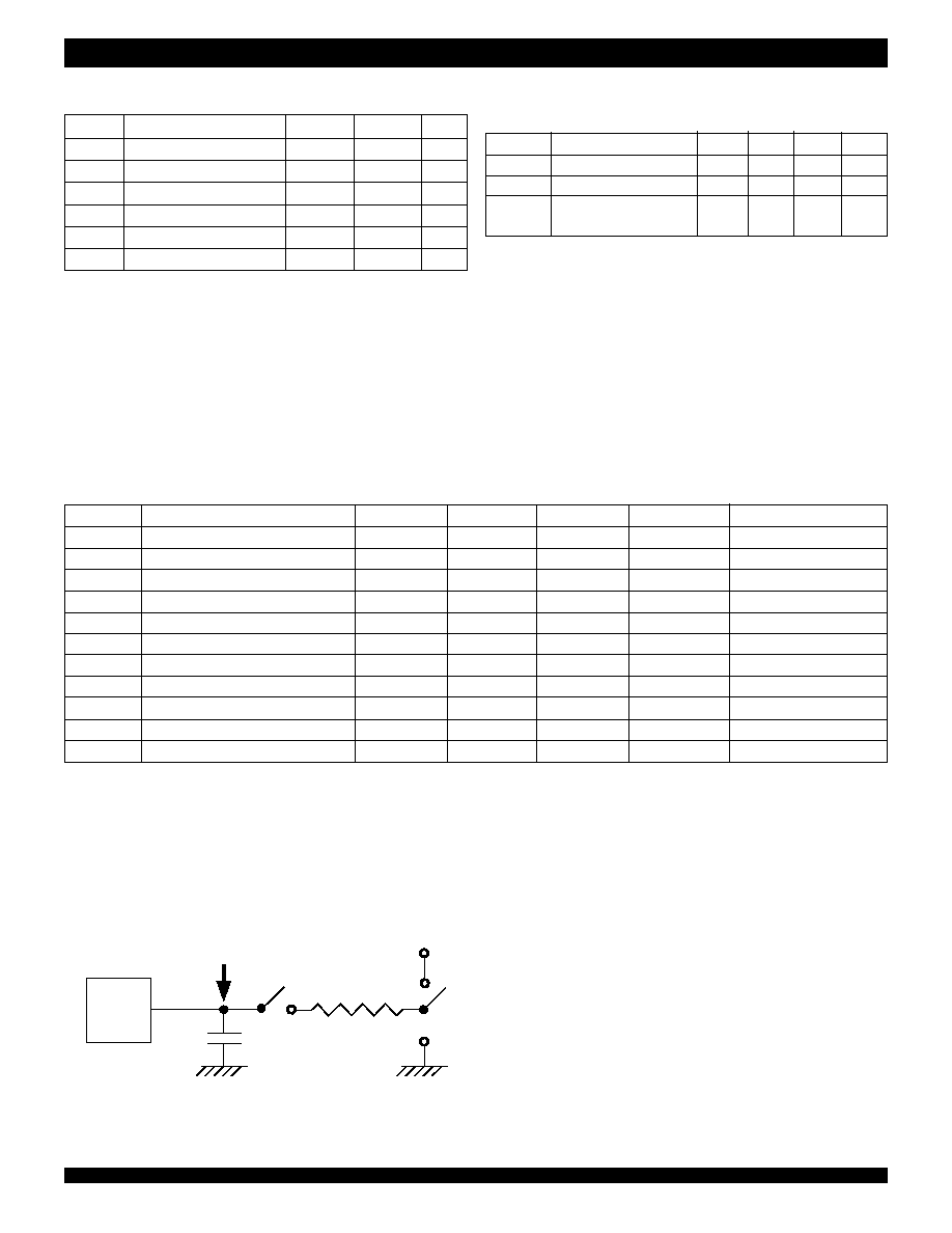
Test Point
Output
Pin
C
L
GND
S
1
R
L
VCC
GND
5706 drw08
S
2
S1 is open circuit except when testing output
levels or high impedance states.
S2 is switched to V
CC
or GND when testing
output levels or high impedance states.
Figure 4. Output Load
RECOMMENDED OPERATING
CONDITIONS
DC ELECTRICAL CHARACTERISTICS
NOTE:
1. Typical figures are at 25
∞
C and are for design aid only; not guaranteed and not subject
to production testing.
NOTE:
1. Typical figures are at 25
∞
C and are for design aid only; not guaranteed and not subject to production testing.
Symbol
Parameter
Min.
Max.
Unit
V
CC
- GND
-0.3
7
V
Vi
Voltage on Digital Inputs
GND - 0.3
V
CC
+0.3
V
V
O
Voltage on Digital Outputs
GND - 0.3
V
CC
+0.3
V
I
O
Current at Digital Outputs
40
mA
T
S
Storage Temperature
-65
+150
∞ C
P
D
Package Power Dissapation
2
W
Symbol
Parameter
Min.
Typ.
(1)
Max.
Unit
V
CC
Positive Supply
4.75
5.25
V
V
I
Input Voltage
0
V
CC
V
T
OP
Operating Temperature
-40
+85
∞
C
Commercial
Symbol
Parameter
Min.
Typ.
(1)
Max.
Units
Test Conditions
I
CC
Supply Current
7
10
mA
Outputs Unloaded
V
IH
Input High Voltage
2.0
V
V
IL
Input Low Voltage
0.8
V
I
IL
Input Leakage
5
µ
A
V
I
between GND and V
CC
C
I
Input Capacitance
8
pF
V
OH
Output High Voltage
2.4
V
I
OH
= 10mA
I
OH
Output High Current
10
15
mA
Sourcing. V
OH
= 2.4V
V
OL
Output Low Voltage
0.4
V
I
OL
= 5mA
I
OL
Output Low Current
5
10
mA
Sinking. V
OL
= 0.4V
I
OZ
High Impedance Leakage
5
µ
A
V
O
between GND and V
CC
C
O
Output Pin Capacitance
8
pF
NOTE:
1. Exceeding these values may cause permanent damage. Functional operation
under these conditions is not implied.
ABSOLUTE MAXIMUM RATINGS
(1)

7
Commercial Temperature Range
IDT728980 Time Slot Interchange
Digital Switch 256 x 256
F0i
Bit Cells
5706 drw09
Channel 31
Bit 0
Channel 0
Bit 7
C4i
Figure 5. Frame Alignment
t
FPH
t
CH
t
FPS
F0i
C4i
5706 drw10
t
CL
t
CHL
t
CTT
t
CLK
t
FPS
t
FPH
t
FPW
(
)
(
)
t
CTT
Figure 6. Clock Timing
AC ELECTRICAL CHARACTERISTICS
(1)
CLOCK TIMING
NOTE:
1. Timing is over recommended temperature and power supply voltages.
2. Typical figures are at 25
∞
C and are for design aid only; not guaranteed and not subject to production testing.
3. Contents of Connection Memory are not lost if the clock stops, however, TX outputs go into the high impedance state.
Symbol
Characteristics
Min.
Typ.
(2)
Max.
Unit
t
CLK
Clock Period
(3)
220
244
300
ns
t
CH
Clock Width High
95
122
150
ns
t
CL
Clock Width Low
110
122
150
ns
t
CTT
Clock Transition Time
20
ns
t
FPS
Frame Pulse Setup Time
20
200
ns
t
FPH
Frame Pulse Hold Time
0.020
50
µ
s
t
FPW
Frame Pulse Width
244
ns

8
Commercial Temperature Range
IDT728980 Time Slot Interchange
Digital Switch 256 x 256
t
TAA
C4i
TX0-7
TX0-7
Bit Cell Boundary
5706 drw11
TX0-7
CCO
t
TOH
t
TAZ
t
TZA
t
XCD
t
XCH
t
TOH
t
OED
ODE
TX0-7
5706 drw12
t
OED
C4i
RX0-7
5706 drw13
Bit Cell Boundaries
t
SIS
t
SIH
Figure 7. Serial Outputs and External Control
Figure 8. Output Driver Enable
Figure 9. Serial Inputs
Symbol
Characteristics
Min.
Typ.
(2)
Max.
Unit
Test Conditions
t
TAZ
TX0-7 Delay - Active to High Z
20
30
60
ns
R
L
= 1K
(3)
, C
L
= 150pF
t
TZA
TX0-7 Delay - High Z to Active
25
45
70
ns
C
L
= 150pF
t
TAA
TX0-7 Delay - Active to Active
30
45
70
ns
C
L
= 150pF
t
TOH
TX0-7 Hold Time
25
45
ns
C
L
= 150pF
t
OED
Output Driver Enable Delay
40
70
ns
R
L
= 1K
(3)
, C
L
= 150pF
t
XCH
External Control Hold Time
0
10
ns
C
L
= 150pF
t
XCD
External Control Delay
20
40
ns
C
L
= 150pF
t
SIS
Serial Input Setup Time
-40
-20
ns
t
SIH
Serial Input Hold Time
90
ns
NOTE:
1. Timing is over recommended temperature and power supply voltages.
2. Typical figures are at 25
∞
C and are for design aid only; not guaranteed and not subject to production testing.
3. High Impedance is measured by pulling to the appropriate rail with R
L
, with timing corrected to cancel time taken to discharge C
L
.
AC ELECTRICAL CHARACTERISTICS
(1)
SERIAL STREAM TIMING

9
Commercial Temperature Range
IDT728980 Time Slot Interchange
Digital Switch 256 x 256
CS
DS
5706 drw14
R/
W
A5-A0
D7-D0
DTA
t
CSS
t
RWS
t
ADS
t
AKD
t
RDS
t
SWD
t
FWS
t
CSH
t
RWH
t
ADH
t
AKH
t
RDZ
t
DHT
Figure 10. Processor Bus
Symbol
Characteristics
Min.
Typ.
(2)
Max.
Unit
Test Conditions
t
CSS
Chip Select Setup Time
10
0
ns
t
RWS
Read/Write Setup Time
10
ns
t
ADS
Address Setup Time
10
ns
t
AKD
Acknowledgment Delay Fast
30
60
ns
C
L
= 150pF
t
AKD
Acknowledgment Delay Slow
2.7
7.2
cycles
C4i cycles
(4)
t
FWS
Fast Write Data Setup Time
20
ns
t
SWD
Slow Write Data Delay
2.0
1.7
cycles
C4i cycles
t
RDS
Read Data Setup Time
0.5
cycles
C4i cycles, C
L
= 150pF
t
DHT
Data Hold Time Read
20
ns
R
L
= 1K
(3)
, C
L
= 150pF
t
DHT
Data Hold Time Write
20
10
ns
t
RDZ
Read Data to High Impedance
30
60
ns
R
L
= 1K
(3)
, C
L
= 150pF
t
CSH
Chip Select Hold Time
0
ns
t
RWH
Read/Write Hold Time
0
ns
t
ADH
Address Hold Time
0
ns
t
AKH
Acknowledgment Hold Time
10
20
40
ns
R
L
= 1K
(3)
, C
L
= 150pF
NOTE:
1. Timing is over recommended temperature and power supply voltages.
2. Typical figures are at 25
∞
C and are for design aid only; not guaranteed and not subject to production testing.
3. High Impedance is measured by pulling to the appropriate rail with R
L
, with timing corrected to cancel time taken to discharge C
L
.
4. Processor accesses are dependent on the
C4i clock, and so some things are expressed as multiples of the C4i.
AC ELECTRICAL CHARACTERISTICS
(1)
PROCESSOR BUS
10
*To search for sales office near you, please click the sales button found on our home page or dial the 800# above and press 2.
The IDT logo is a registered trademark of Integrated Device Technology, Inc. and the ST-BUS
Æ
is a trademark of Mitel Corp.
CORPORATE HEADQUARTERS
for SALES:
for Tech Support:
2975 Stender Way
800-345-7015 or 408-727-6116
408-330-1753
Santa Clara, CA 95054
fax: 408-492-8674
email: FIFOhelp@idt.com
www.idt.com*
P Pkg: www.idt.com/docs/PSC4003.pdf
J Pkg: www.idt.com/docs/PSC4008.pdf
DB Pkg: www.idt.com/docs/PSC4082.pdf
5706 drw15
XXXXXX
IDT
Device Type
X
Package
Process/
Temperature
Range
XX
BLANK
Commercial (-40
∞
C to +85
∞
C)
728980
256 x 256
Time Slot Interchange Digital Switch
J
Plastic Leaded Chip Carrier (PLCC, J44-1)
P
DB
Plastic Dip (P40-1)
Plastic Quad Flatpack (PQFP, DB44-1)
ORDERING IN.ORMATION
DATASHEET DOCUMENT HISTORY
5/23/2000
pgs. 1, 2, and 10.
8/18/2000
pgs. 1, 2, and 10.
01/24/2001
pgs. 1 and 6.