 | –≠–ª–µ–∫—Ç—Ä–æ–Ω–Ω—ã–π –∫–æ–º–ø–æ–Ω–µ–Ω—Ç: 728985 | –°–∫–∞—á–∞—Ç—å:  PDF PDF  ZIP ZIP |
1
2001 Integrated Device Technology, Inc.
APRIL 2001
TIME SLOT INTERCHANGE
DIGITAL SWITCH
256 x 256
IDT728985
DSC-5708/2
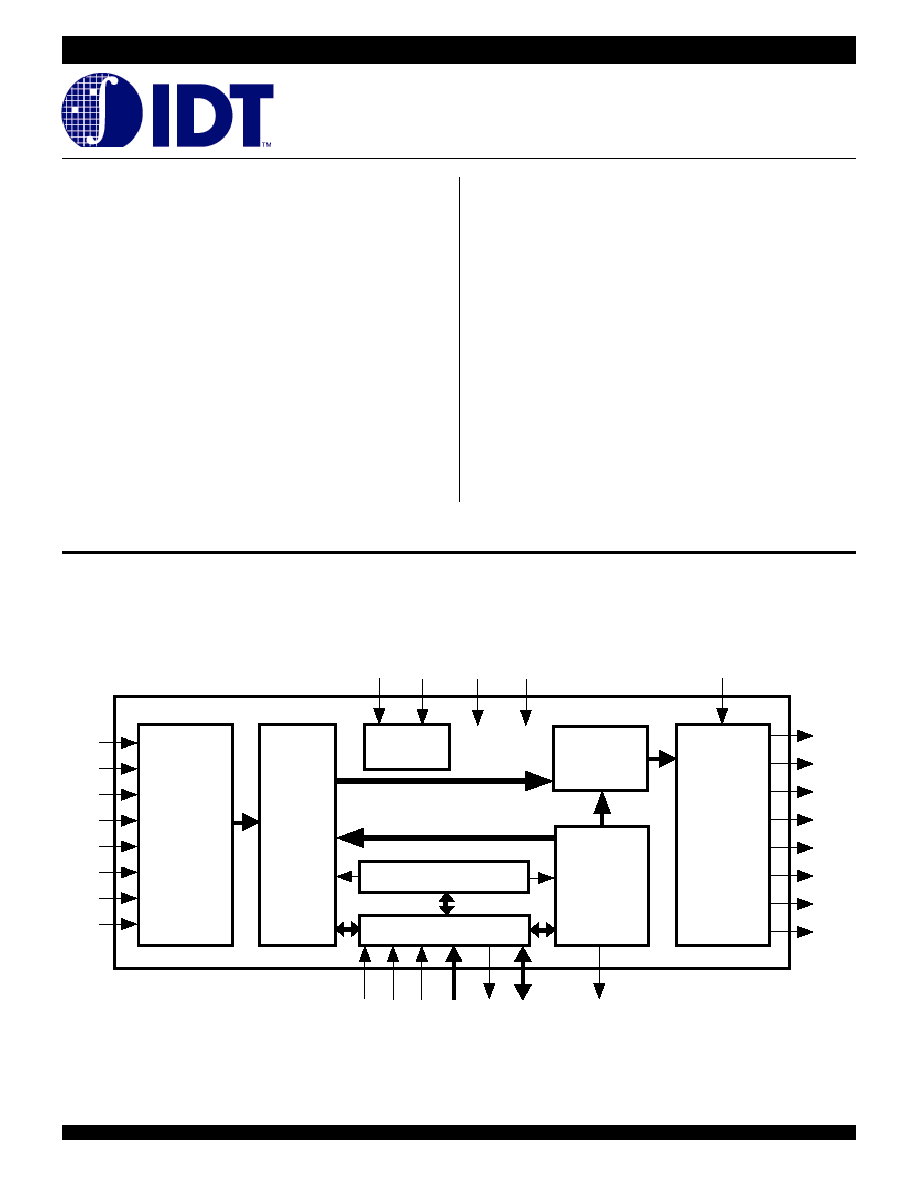
.UNCTIONAL BLOCK DIAGRAM
.EATURES:
∑
∑
∑
∑
∑
256 x 256 channel non-blocking switch
∑
∑
∑
∑
∑
Automatic signal identification (ST-BUS
Æ
, GCI)
∑
∑
∑
∑
∑
8 RX inputs -- 32 channels at 64 Kbit/s per serial line
∑
∑
∑
∑
∑
8 TX outputs -- 32 channels at 64 Kbit/s per serial line
∑
∑
∑
∑
∑
Three-state serial outputs
∑
Microprocessor Interface (8-bit data bus)
∑
∑
∑
∑
∑
Frame Integrity for data applications
∑
∑
∑
∑
∑
5V Power Supply
∑
∑
∑
∑
∑
Operating Temperature Range -40
∞∞
∞∞
∞
C to +85
∞∞
∞∞
∞
C
∑
∑
∑
∑
∑
Available in 44-pin Plastic Leaded Chip Carrier (PLCC),
44-pin Plastic Quad Flatpack (PQFP) and 40-pin Plastic Dip
(P-DIP)
DESCRIPTION:
The IDT728985 is a ST-BUS
Æ
/GCI compatible digital switch controlled by
a microprocessor. The IDT728985 can handle as many as 256, 64 Kbit/s input
and output channels. Those 256 channels are divided into 8 serial inputs and
outputs, each of which consists of 32 channels. The IDT728985 provides per-
channel variable or constant throughput delay modes and microprocessor read
and write access to individual channels. As an important function of a digital
switch is to maintain sequence integrity and minimize throughput delay, the
IDT728985 is an ideal solution for most switching needs.
.UNCTIONAL DESCRIPTION
Frame sequence, constant throughput delay, and guaranteed minimum
delay are high priority requirements in today's integrated data and multimedia
networks. The IDT728985 provides these functions on a per-channel basis
using a standard microprocessor control interface. Each of the eight serial lines
is designed to switch 64 Kbit/s PCM or N x 64 Kbit/s data.
In Processor Mode, the microprocessor can access the input and output time
slots to control other devices such as ISDN transceivers and trunk interfaces.
Supporting both GCI and ST-BUS
Æ
formats, IDT728985 has incorporated an
internal circuit to automatically identify the polarity and format of the frame
synchronization.
A functional block diagram of the IDT728985 device is shown on page 1.
The serial streams operate continuously at 2.048 Mb/s and are arranged in
125
µ
s wide frames each containing 32, 8-bit channels. Eight input (RX0-7) and
Microprocessor Interface
Control Register
Timing
Unit
RX0
RX1
RX2
RX3
RX4
RX5
RX6
RX7
TX0
TX1
TX2
TX3
TX4
TX5
TX6
TX7
ODE
F0i
C4i
V
CC
CS
DS
R/
W
A0/
A5
GND
CCO
DTA
D0/
D7
5708 drw01
Receive
Serial Data
Streams
Data
Memory
Output MUX
Connection
Memory
Transmit
Serial Data
Streams
2
Commercial Temperature Range
IDT728985 Time Slot Interchange
Digital Switch 256 x 256
35
34
33
32
31
30
29
37
36
3
2
44
1
43
42
41
5
4
6
5708 drw02
INDEX
38
39
40
21
22
24
23
25
26
27
19
20
18
28
DS
CS
R/
W
11
12
13
14
15
16
17
9
10
8
7
RX2
RX1
RX0
DTA
TX0
TX1
TX2
DNC
(1)
CCO
ODE
TX3
TX4
TX5
TX6
TX7
GND
D
0
RX3
RX4
RX5
RX6
RX7
V
CC
F0i
C4i
A
0
D
1
D
2
D
3
D
4
A
1
A
2
DNC
(1)
DNC
(1)
DNC
(1)
D
5
D
6
D
7
A
5
A
4
A
3
DTA
CCO
ODE
1
2
40
39
TX0
3
38
TX1
4
37
TX2
5
36
TX3
6
35
TX4
7
34
TX5
8
33
TX6
9
32
TX7
10
31
GND
11
30
D
0
12
29
CS
13
28
14
27
5708 drw04
15
16
17
18
19
20
26
25
24
23
22
21
RX1
RX2
RX3
RX4
RX5
RX6
F0i
A
0
R/
W
DS
C4i
V
CC
RX7
RX0
D
1
D
2
D
3
D
4
D
5
D
6
D
7
A
1
A
2
A
3
A
4
A
5
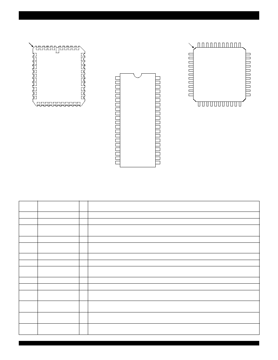
PIN CON.IGURATION
PIN DESCRIPTIONS
PLCC: 0.05in. pitch, 0.65in. x 0.65in.
(J44-1, order code: J)
TOP VIEW
PLASTIC DIP: 0.10in. pitch, 2.05in. x 0.60in.
(P40-1, order code: P)
TOP VIEW
29
28
27
26
25
24
23
31
30
44
43
42
41
5708 drw03
INDEX
32
33
40
DS
CS
R/
W
5
6
7
8
9
10
11
3
4
2
1
RX2
RX1
RX0
DTA
TX0
TX1
TX2
DNC
(1)
CCO
ODE
TX3
TX4
TX5
TX6
TX7
GND
D
0
RX3
RX4
RX5
RX6
RX7
V
CC
F0i
C4i
A
0
D
1
D
2
D
3
D
4
A
1
A
2
DNC
(1)
DNC
(1)
DNC
(1)
D
5
D
6
D
7
A
5
A
4
A
3
39
38
37
36
35
34
12
13
14
15
16
17
18
19
20
21
22
PQFP: 0.80mm pitch, 10mm x 10mm
(DB44-1, order code: DB)
TOP VIEW
NOTE:
1. DNC - Do Not Connect
SYMBOL
NAME
I/O
DESCRIPTION
GND
Ground.
Ground Rail.
V
CC
V
CC
+5.0 Volt Power Supply.
DTA
Data Acknowledgment
O
This active LOW output indicates that a data bus transfer is complete. A pull-up resistor is required at this
(Open Drain)
output.
RX0-7
RX Input 0 to 7
I
Serial data input streams. These streams have 32 channels at data rates of 2.048 Mb/s.
F0i
Frame Pulse
I
This input accepts and automatically identifies frame synchronization signals formatted according to different
backplane specifications such as ST-BUS
Æ
and
GCI.
C4i
Clock
I
4.096 MHz serial clock for shifting data in and out of the data streams.
A0-A5
Address 0 to 5
I
These lines provide the address to IDT728985 internal registers.
DS
Data Strobe
I
This is the input for the active HIGH data strobe on the microprocessor interface. This input operates with
CS to enable the internal read and write generation.
R/
W
Read/Write
I
This input controls the direction of the data bus lines (D0-D7) during a microprocessor access.
CS
Chip Select
I
Active LOW input enabling a microprocessor read or write of control register or internal memories.
D0-D7
Data Bus 0 to 7
I/O
These pins provide microprocessor access to data in the internal control register. Connection Memory HIGH,
Connection Memory LOW and data memory.
TX0-7
TX Outputs 0 to 7
O
Serial data output streams. These streams are composed of 32, 64 Kbit/s channels at data rates of 2.048 Mb/s.
(Three-state Outputs)
ODE
Output Drive Enable
I
This is an output enable for the TX0-7 serial outputs. If this input is LOW, TX0-7 are high-impedance. If this is
HIGH, each channel may still be put into high-impedance by software control.
CCO
Control Channel Output
O
This output is a 2.048 Mb/s line which contains 256 bits per frame. The level of each bit is controlled by the
contents of the CCO bit in the Connection Memory HIGH locations.
3
Commercial Temperature Range
IDT728985 Time Slot Interchange
Digital Switch 256 x 256
eight output (TX0-7) serial streams are provided in the IDT728985 device
allowing a complete 256 x 256 channel non-blocking switch matrix to be
constructed. The serial interface clock for the device is 4.096 MHz, as required
in ST-BUS
Æ
and GCI specifications.
The received serial data is internally converted to parallel by the on chip
serial-to-parallel converters and stored sequentially in a 256-position Data
Memory. By using an internal counter that is reset by the input 8 KHz frame pulse,
F0i, the incoming serial data streams can be framed and sequentially addressed.
Depending on the type of information to be switched, the IDT728985 device
can be programmed to perform time slot interchange functions with different
throughput delay capabilities on a per-channel basis. The Variable Delay
mode, most commonly used for voice applications, can be selected ensuring
minimum throughput delay between input and output data. In Constant Delay
mode, used in multiple or grouped channel data applications, the integrity of the
information through the switch is maintained.
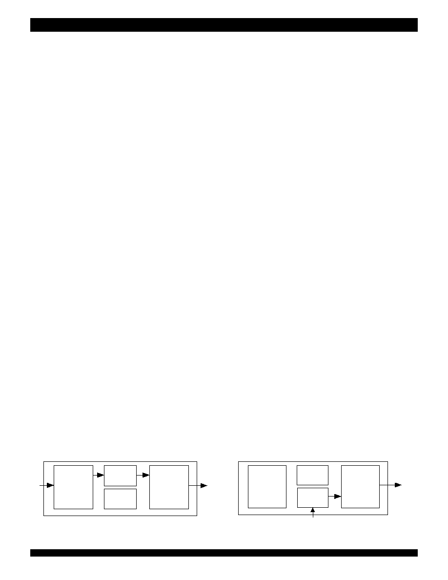
CONNECTION MEMORY
Data to be output on the serial streams may come from two sources: Data
Memory or Connection Memory. The Connection Memory is split into HIGH
and LOW parts and is associated with particular TX output streams. In Processor
Mode, data output on the TX streams is taken from the Connection Memory Low
and originates from the microprocessor (Figure 2). Where as in Connection
Mode (Figure 1), data is read from Data Memory and originated from the
incoming RX streams. Data destined for a particular channel on the serial output
stream is read internally during the previous channel time slot to allow time for
memory access and internal parallel-to-serial conversion.
CONNECTION MODE
In Connection Mode, the addresses of input source for all output channels
are stored in the Connection Memory Low. The Connection Memory Low
locations are mapped to corresponding 8-bit x 32-channel outputs. The contents
of the Data Memory at the selected address are then transferred to the parallel-
to-serial converters before being output. By having the output channel to specify
the input channel through the Connection Memory, the same input channel can
be broadcast to several output channels.
PROCESSOR MODE
In Processor Mode the CPU writes data to the Connection Memory Low
locations which correspond to the output link and channel number. The contents
of the Connection Memory Low are transferred to the parallel-to-serial
converter one channel before it is to be output and are transmitted each frame
to the output until it is changed by the CPU.
CONTROL
The Connection Memory High bits (Table 4) control the per-channel
functions available in the IDT728985. Output channels are selected into specific
modes such as: Processor Mode or Connection mode, Variable or Constant
throughput delay modes, Output Drivers Enabled or in three-state condition.
There is also one bit to control the state of the CCO output pin.
OUTPUT DRIVE ENABLE (ODE)
The ODE pin is the master output three-state control pin. If the ODE input
is held LOW all TDM (Time Division Multiplexed) outputs will be placed in high
impedance regardless Connection Memory High programming. However, if
ODE is HIGH, the contents of Connection Memory High control the output state
on a per-channel basis.
SERIAL INTERFACE TIMING
The IDT728985 master clock (
C4i) is 4.096 MHz signal allowing serial data
link configuration at 2.048 Mb/s to be implemented. The IDT728985 can
automatically detect the presence of an input frame pulse, identify the type of
backplane present on the serial interface, and format the synchronization pulse
according to ST-BUS
Æ
or GCI interface specifications (active HIGH in GCI or
active LOW in ST-BUS
Æ
). Upon determining the correct interface Connected
to the serial port, the internal timing unit establishes the appropriate serial data
bit transmit and sampling edges. In ST-BUS
Æ
mode, every second falling edge
of the 4.096 MHz clock marks a boundary and the input data is clocked in by
the rising edge, three quarters of the way into the bit cell. In GCI mode every
second rising edge of the 4.096 MHz clock marks the bit boundary while data
sampling is performed during the falling edge, at three quarters of the bit
boundaries.
DELAY THROUGH THE IDT728985
The transfer of information from the input serial streams to the output serial
streams results in a delay through the device. The delay through the IDT728985
device varies according to the mode selected in the
V/C bit of the Connection
Memory High.
VARIABLE DELAY MODE
The delay in Variable Delay Mode is dependent only on the combination
of source and destination on the input and output streams. The minimum delay
achievable in the IDT728985 device is three time slots. In the IDT728985
device, the information that is to be output in the same channel position as the
information is input (position n), relative to frame pulse, will be output in the
following frame (channel n, frame n+1). The same occurs if the input channels
succeeding (n+1, n+2) the channel position as the information is input.
The information switched to the third time slot after the input has entered the
device (for instance, input channel 0 to output channel 3 or input channel 30 to
output channel 1), is always output three channels later.
Any switching configuration that provides three or more time slots between
input and output channels, will have a throughput delay equal to the difference
Figure 2. Processor Mode
Figure 1. Connection Mode
Receive
Serial Data
Streams
5708 drw05
RX
TX
Transmit
Serial Data
Streams
Data
Memory
Connection
Memory
5708 drw06
TX
Microprocessor
Receive
Serial Data
Streams
Transmit
Serial Data
Streams
Data
Memory
Connection
Memory
.UNCTIONAL DESCRIPTION (Cont'd)
4
Commercial Temperature Range
IDT728985 Time Slot Interchange
Digital Switch 256 x 256
between the output and input channels; i.e., the throughput delay will be less
than one frame. Table 1 shows the possible delays for the IDT728985 device
in Variable Delay Mode. An example is shown in Figure 3.
CONSTANT DELAY MODE
In this mode frame integrity is maintained in all switching configurations by
making use of a multiple Data Memory buffer technique where input channels
written in any of the buffers during frame N will be read out during frame N+2.
In the IDT728985, the minimum throughput delay achievable in Constant Delay
mode will be 32 time slots; for example, when input time slot 32 (channel 31) is
switched to output time slot 1 (channel 0). Likewise, the maximum delay is
achieved when the first time slot in a frame (channel 0) is switched to the last time
slot in the frame (channel 31), resulting in 94 time slots of delay (see Figure 4).
To summarize, any input time slot from input frame N will be always switched
to the destination time slot on output frame N+2. In Constant Delay mode the
device throughput delay is calculated according to the following formula:
DELAY=[32+(32-IN)+(OUT-1)]
IN =the number of the input time slot (from 1 to 32)
OUT = the number of the output time slot (from 1 to 32).
MICROPROCESSOR PORT
The IDT728985 microprocessor port is a non-multiplexed bus architecture.
The parallel port consists of an 8-bit parallel data bus (D0-D7), six address input
lines (A0-A5) and four control lines (
CS, DS, R/W and DTA). This parallel
microport allows the access to the Control Registers, Connection Memory Low,
Connection Memory High, and the Data Memory. All locations are read/written
except for the Data Memory, which can be read only.
Accesses from the microport to the Connection Memory and the Data
Memory are multiplexed with accesses from the input and output TDM ports.
This can cause variable Data Acknowledge delays (
DTA). In the IDT728985
device, the
DTA output provides a maximum acknowledgment delay of 800ns
for read/write operations in the Connection Memory. However, for operations
in the Data Memory (Processor Mode), the maximum acknowledgment delay
can be 1220ns.
SO.TWARE CONTROL
If the A5, A1, A0 address line inputs are LOW then the IDT728985 Internal
Control Register is addressed (see Table 2). If A5 input line is high, then the
remaining address input lines are used to select the 32 possible channels per
input or output stream. As explained in the Control Register description, the
address input lines and the Stream Address bits (STA) of the Control register
give the user the capability of selecting all positions of IDT728985 Data and
Connect memories. See Figure 6 for accessing internal memories.
The data in the control register consists of Memory Select and Stream
Address bits, Split Memory and Processor Enable bits (Table 3). In Split Memory
mode (Bit 7 of the Control register) reads are from the Data Memory and writes
are to the Connection Memory LOW. The Memory Select bits allow the
Connection Memory High or LOW or the Data Memory to be chosen, and the
Stream Address bits define internal memory subsections corresponding to input
or output streams.
The Processor Enable bit (bit 6) places every output channel on every
output stream in Processor Mode; i.e., the contents of the Connection Memory
LOW (CML, Table 5) are output on the output streams once every frame unless
the ODE input pin is LOW. If PE bit is HIGH, then the IDT728985 behaves as
if bits 2 (Channel Source) and 0 (Output Enable) of every Connection Memory
High (CMH) locations were set to HIGH, regardless of the actual value. If PE
is LOW, then bit 2 and 0 of each Connection Memory High location operates
normally. In this case, if bit 2 of the CMH is HIGH, the associated TX output
channel is in Processor Mode. If bit 2 of the CMH is LOW, then the contents of
the CML define the source information (stream and channel) of the time slot that
is to be switched to an output, Table 4.
If the ODE input pin is LOW, then all the serial outputs are high-impedance.
If ODE is HIGH, then bit 0 (Output Enable) of the CMH location enables (if HIGH)
or disables (if LOW) for that particular channel.
The contents of bit 1 (CCO) of each Connection Memory High Location (see
Table 4) is output on CCO pin once every frame. The CCO pin is a 2.048 Mb/s
output, which carries 256 bits. If CCO bit is set HIGH, the corresponding bit on
CCO output is transmitted HIGH. If CCO is LOW, the corresponding bit on the
CCO output is transmitted LOW. The contents of the 256 CCO bits of the CMH
are transmitted sequentially on to the CCO output pin and are synchronous to
the TX streams. To allow for delay in any external control circuitry the contents
of the CCO bit is output one channel before the corresponding channel on the
TX streams. For example, the contents of CCO bit in position 0 (corresponding
to TX0, CH0), is transmitted synchronously with the TX channel 31, bit 7. Bit 1's
of CMH for channel 1 of streams 0-7 are output synchronously with TX channel
0 bits 7-0.
INITIALIZATION
During the microprocessor initialization routine, the microprocessor should
program the desired active paths through the matrices, and put all other channels
into the high impedance state. Care should be taken that no two Connected TX
outputs drive the bus simultaneously. The ODE pin should be held low on power
up to keep all output pins in high-impedance. With the CMH setup, the
microprocessor controlling the matrices can bring the ODE signal high to
relinquish high impedance state control to the Connection Memory High bits
outputs.
TABLE 2
ADDRESS MAPPING
A5
A4
A3
A2
A1
A0
LOCATION
0
X
X
X
0
0
Control Register
(1)
1
0
0
0
0
0
Channel 0
(2)
1
0
0
0
0
1
Channel 1
(2)
1
∑
∑
∑
∑
∑
∑
1
∑
∑
∑
∑
∑
∑
1
∑
∑
∑
∑
∑
∑
1
∑
∑
∑
∑
∑
∑
1
∑
∑
∑
∑
∑
∑
1
1
1
1
1
1
Channel 31
(2)
TABLE 1
VARIABLE DELAY MODE
Input Channel
Output Channel
Throughput Delay
n
m=n, n+1 or n+2
m-n+32 time slot
n
m>n+2
m-n time slot
n
m<n
32-(n-m) time slot

5
Commercial Temperature Range
IDT728985 Time Slot Interchange
Digital Switch 256 x 256
For Slot 1 ("A"): IN=32, OUT=1, DELAY=(32-32)+32+(1-1)=32 time slots minimum delay
For Slot 32 ("J"): IN=1, OUT=32, DELAY=(32-1)+32+(32-1)=94 time slots maximum delay
Figure 4. Constant Delay Mode
A B C D E F G H I J
J J J
G H
I J
32 Slots
32 Slots
32 Slots
32 31.........7 6 5 4 3 2 1 Time Slot
Outgoing Now
Incoming Now
Outgoing Next
32 31........7 6 5 4 3 2 1
32 Slots
32 Slots
32 Slots
5708 drw07
Outgoing
Incoming
Switching
J I H G F E D C B A
Time Slot 32 31 30 29 28............ 3 2 1
32 31 30 29 28............. 3 2 1 Time Slot
A B C D E F G H I J
Time Slot 32 31 30 29 28............ 3 2 1
Figure 3. Variable Delay Mode
For J: DELAY=3 Slots, 32 Slots, 33 Slots, and 34 Slots
For G, H, and I: DELAY= 3 slots
6
Commercial Temperature Range
IDT728985 Time Slot Interchange
Digital Switch 256 x 256
Connection Memory High
Connection Memory Low
0
1
1
0
1
1
Control Register
CR
b
7
5708 drw08
The Control Register is only accessed when A5=0.
All other address bits have no effect when A5=0.
When A5 =1, only 32 bytes are randomly accessable via
A0-A4 at any one instant. Which 32 bytes are
accessed is determined by the state of CRb0 -CRb4.
The 32 bytes correlate to 32 channel of one ST-BUS
stream.
CR
b
6
CR
b
5
CR
b
4
CR
b
3
CR
b
2
CR
b
1
CR
b
0
CR
b
4
CR
b
3
0
0
0
0
0
0
1
1
0
1
0
2
0
1
1
3
1
0
0
4
1
0
1
5
1
1
0
6
1
1
1
7
Stream
CR
b
2
CR
b
1
CR
b
0
100001
100010
100000
Channel 0
Channel 1
Channel 2
Channel 0
Channel 1
Channel 2
Channel 0
Channel 1
Channel 2
Channel 0
Channel 1
Channel 2
Channel 0
Channel 1
Channel 2
Channel 0
Channel 1
Channel 2
Channel 0
Channel 1
Channel 2
Channel 0
Channel 1
Channel 2
111111
External Address Bits
A5-A0
Channel 31
Channel 31
Channel 31
Channel 31
Channel 31
Channel 31
Channel 31
Channel 31
Data Memory
Figure 6. Addressing Internal Memories
7
Commercial Temperature Range
IDT728985 Time Slot Interchange
Digital Switch 256 x 256
TABLE 4
CONNECTION MEMORY HIGH
TABLE 5
CONNECTION MEMORY LOW
TABLE 3
CONTROL REGISTER
Bit
Name
Description
7
SM (Split Memory)
When 1, all subsequent reads are from the Data Memory and writes are to the Connection Memory, except when
the Control Register is accessed again. The Memory Select bits need to specify the memory for the operations.
6
PE (Processor Mode)
When 1, the contents of the Connection Memory LOW are output on the Serial Output streams except when in high-
impedance. When 0, the Connection Memory bits for each channel determine what is output.
5
unused
4-3
MS1-MS0
0-0 - Not to be used.
(Memory Select Bits)
0-1 - Data Memory (read only from the CPU)
1-0 - Connection Memory LOW
1-1 - Connection Memory is HIGH
2-0
STA2-0
The number expressed in binary notation on these bits refers to the input or output stream which corresponds to the
(Stream Address Bits)
subsection of memory made accessible for subsequent operations.
SM
PE
X
MS1
MS0
STA2
STA1
STA0
7
6
5
4
3
2
1
0
x = don't care
x = don't care
Bit
Name
Description
7,5,4,3
unused
6
V/C (Variable/Constant
This bit is used to select between Variable (LOW) and Constant Delay (HIGH) modes on a per-channel basis.
Throughput Delay Mode)
2
CS
When 1, the contents of the corresponding location in Connection Memory LOW are output on the location's channel
(Channel Source)
and stream. When 0, the contents of the corresponding location in Connection Memory LOW act as an address for the
Data Memory and determine the source of the connection to the location's channel and stream.
1
CCO (CCO Bit)
This bit drives a bit time on the CCO output pin.
0
OE (Output Enable)
This bit enables the output drivers on a per-channel basis. This allows individual channels on individual streams to
be made high-impedance, allowing switch matrices to be constructed. A HIGH enables the driver and a LOW disables it.
X
V/C
X
X
X
CS
CCO
OE
7
6
5
4
3
2
1
0
Bit
Name
Description
7-5
SAB2-0
(1)
These three bits are used to select eight source streams for the Connection.
(Source Stream Address Bits)
4-0
(1)
CAB2-0
(1)
These five bits are used to select 32 different source channels for the Connection (the stream where the channel
(Source Channel Address Bits) is present is defined by bits SAB2-0). Bit 4 is the most significant bit.
SAB2
SAB1
SAB0
CAB4
CAB3
CAB2
CAB1
CAB0
NOTE:
1. If bit 2 of the corresponding Connection HIGH location is 1 or bit 6 of the Control Register is 1, then these entire 8 bits are output on the channel and stream associated with
this location. Otherwise, the bits are used as indicated to define the source of the Connection which is output on the channel and stream associated with this location.
7
6
5
4
3
2
1
0
8
Commercial Temperature Range
IDT728985 Time Slot Interchange
Digital Switch 256 x 256
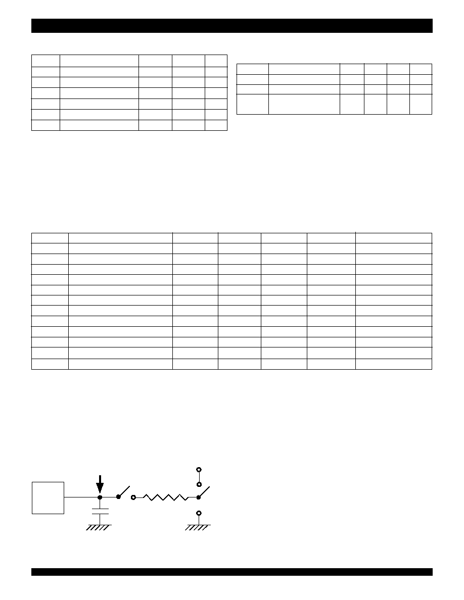
Test Point
Output
Pin
C
L
GND
S
1
R
L
VCC
GND
5708 drw09
S
2
S1 is open circuit except when testing output
levels or high impedance states.
S2 is switched to V
CC
or GND when testing
output levels or high impedance states.
Figure 6. Output Load
RECOMMENDED OPERATING
CONDITIONS
DC ELECTRICAL CHARACTERISTICS
NOTE:
1. Typical figures are at 25
∞
C and are for design aid only; not guaranteed and not subject
to production testing.
NOTE:
1. Typical figures are at 25
∞
C and are for design aid only; not guaranteed and not subject to production testing.
Symbol
Parameter
Min.
Max.
Unit
V
CC
- GND
-0.3
7
V
Vi
Voltage on Digital Inputs
GND - 0.3
V
CC
+0.3
V
V
O
Voltage on Digital Outputs
GND - 0.3
V
CC
+0.3
V
I
O
Current at Digital Outputs
40
mA
T
S
Storage Temperature
-65
+150
∞ C
P
D
Package Power Dissapation
2
W
Symbol
Parameter
Min.
Typ.
(1)
Max.
Unit
V
CC
Positive Supply
4.75
5.0
5.25
V
V
I
Input Voltage
0
V
CC
V
T
OP
Operating Temperature
-40
25
+85
∞
C
Commercial
Symbol
Parameter
Min.
Typ.
(1)
Max.
Units
Test Conditions
I
CC
Supply Current
7
10
mA
Outputs Unloaded
V
IH
Input High Voltage
2.0
V
V
IL
Input Low Voltage
0.8
V
I
IL
Input Leakage (Inputs)
5
µ
A
V
I
between GND and V
CC
I
IL
Input Leakage (I/O pins)
34
100
µ
A
C
I
Input Capacitance
8
pF
V
OH
Output High Voltage
2.4
V
I
OH
= 10mA
I
OH
Output High Current
10
15
mA
Sourcing. V
OH
= 2.4V
V
OL
Output Low Voltage
0.4
V
I
OL
= 5mA
I
OL
Output Low Current
5
10
mA
Sinking. V
OL
= 0.4V
I
OZ
High Impedance Leakage
5
µ
A
V
O
between GND and V
CC
C
O
Output Pin Capacitance
8
pF
NOTE:
1. Exceeding these values may cause permanent damage. Functional operation under
these conditions is not implied.
ABSOLUTE MAXIMUM RATINGS
(1)

9
Commercial Temperature Range
IDT728985 Time Slot Interchange
Digital Switch 256 x 256
AC ELECTRICAL CHARACTERISTICS
(1)
ST-BUS
Æ
TIMING
Figure 7. ST-BUS
Æ
Timing
F0i
C4i
TX
RX
5708 drw 10
Ch. 31, Bit 0
Ch. 0, Bit 7
Ch. 0, Bit 6
Ch. 0, Bit 6
Ch. 0, Bit 7
Ch. 31, Bit 0
Ch. 0,
Bit 5
t
F0iW
Ch. 0, Bit 5
t
F0iH
t
F0iS
t
DAA
t
C4i
t
STiS
t
STiH
t
CH
t
CL
t
f
t
r
NOTE:
1. Timing is over recommended temperature and power supply voltages (V
CC
=5V
±
5%, GND=0V, TA=40
∞
C to 85
∞
C).
2. Typical figures are at 25
∞
C and are for design aid only; not guaranteed and not subject to production testing.
Symbol
Parameter
Min.
Typ.
(2)
Max.
Units
Test Conditions
t
F0iW
Frame Pulse Width
244
ns
Outputs Loaded
t
F0iS
Frame Pulse Setup Time
10
190
ns
t
F0iH
Frame Pulse Hold Time
20
190
ns
t
DAA
TX delay Active to Active
40
60
ns
C
L
= 150pF
t
STiS
RX Setup Time
20
ns
t
STiH
RX Hold Time
20
ns
t
C4i
Clock Period
200
244
300
ns
t
CL
CK Input Low
85
122
150
ns
t
CH
CK Input High
85
122
150
ns
t
r,
t
f
Clock Rise/Fall Time
10
ns
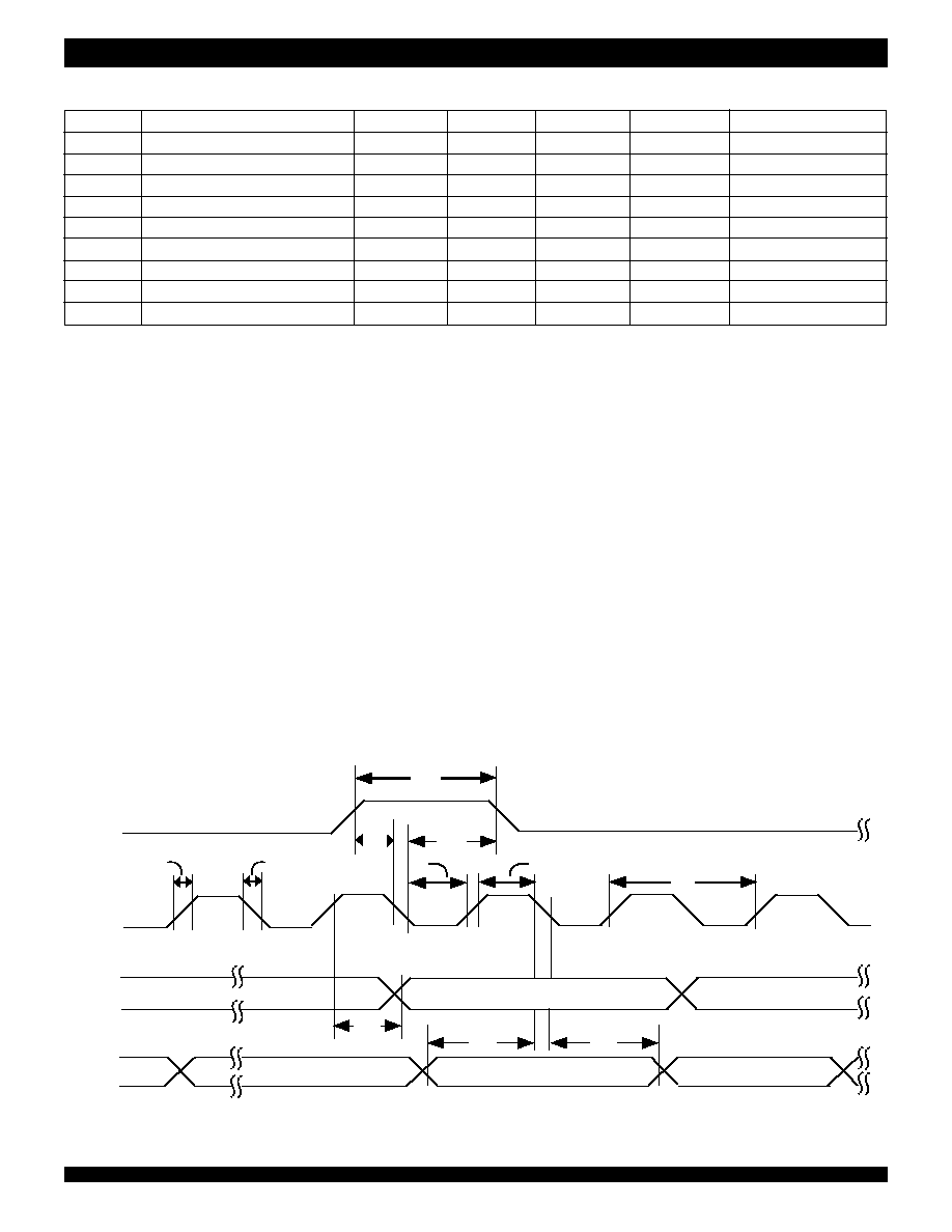
10
Commercial Temperature Range
IDT728985 Time Slot Interchange
Digital Switch 256 x 256
Figure 8. GCI Timing
t
DAA
TX
RX
5708 drw11
t
STiS
t
STiH
t
WFH
F0i
C4i
t
CH
t
CL
t
f
t
r
t
C4i
Ch. 31
Bit 7
Ch. 0
Bit 0
Ch. 0
Bit 1
Ch. 0
Ch. 0
Bit 1
Bit 0
Ch. 31
Bit 7
t
F0iS
t
F0iH
AC ELECTRICAL CHARACTERISTICS
(1)
GCI TIMING
NOTE:
1. Timing is over recommended temperature and power supply voltages (V
CC
=5V
±
5%, GND=0V, TA=40
∞
C to 85
∞
C).
2. Typical figures are at 25
∞
C and are for design aid only; not guaranteed and not subject to production testing.
Symbol
Parameter
Min.
Typ.
(2)
Max.
Units
Test Conditions
t
C4i
Clock Period
150
244
300
ns
Outputs Loaded
tCL, tCH
Pulse Width
73
122
150
ns
t
WFH
Frame Width High
244
ns
t
F0iS
Frame Setup
10
190
ns
t
F0iH
Frame Hold
20
190
ns
t
DAA
Data Delay/Clock Active to Active
40
60
ns
C
L
= 150pF
t
STiS
Serial Input Setup
20
ns
t
STiH
Serial Input Hold
20
ns
t
r,
t
f
Clock Rise/Fall Time
10
ns
11
Commercial Temperature Range
IDT728985 Time Slot Interchange
Digital Switch 256 x 256
C4i
TX0-7
CCO
5708 drw12
TX0-7
(GCI)
(ST-BUS
)
Bit Cell Boundary
t
TAZ
t
XCD
t
TZA
Figure 9. Serial Outputs and External Control
Figure 10. Output Driver Enable
t
OED
ODE
TX0-7
5708 drw13
t
OED
AC ELECTRICAL CHARACTERISTICS
(1)
SERIAL STREAM TIMING
Symbol
Characteristics
Min.
Typ.
(2)
Max.
Unit
Test Conditions
t
TAZ
TX0-7 Delay - Active to High Z
40
60
ns
R
L
= 1K
(3)
, C
L
= 150pF
t
TZA
TX0-7 Delay - High Z to Active
40
60
ns
C
L
= 150pF
t
OED
Output Driver Enable Delay
40
60
ns
R
L
= 1K
(3)
, C
L
= 150pF
t
XCD
CCO Output Delay
0
20
40
ns
C
L
= 150pF
NOTE:
1. Timing is over recommended temperature and power supply voltages.
2. Typical figures are at 25
∞
C and are for design aid only; not guaranteed and not subject to production testing.
3. High Impedance is measured by pulling to the appropriate rail with R
L
, with timing corrected to cancel time taken to discharge C
L
.
12
Commercial Temperature Range
IDT728985 Time Slot Interchange
Digital Switch 256 x 256
Figure 11. Motorola Non-Multiplexed Bus Timing
CS
DS
D0-D7
WRITE
5708 drw14
R/
W
A0-A5
D0-D7
READ
DTA
VALID DATA
VALID DATA
t
CSS
t
RWS
t
ADS
t
CSH
t
RWH
t
ADH
t
DHR
t
DSW
t
SWD
t
DDR
t
AKD
t
DHW
t
AKH
AC ELECTRICAL CHARACTERISTICS
(1)
MICROPROCESSOR TIMING
Symbol
Characteristics
Min.
Typ.
(2)
Max.
Unit
Test Conditions
t
CSS
CS Setup from DS Rising
0
ns
t
RWS
R/
W Setup from DS Rising
5
ns
t
ADS
Add Setup from DS Rising
5
ns
t
CSH
CS Hold after DS Falling
0
ns
t
RWH
R/
W Hold after DS Falling
5
ns
t
ADH
Add Hold after DS Falling
5
ns
t
DDR
Data Setup from
DTA Low on Read
10
ns
C
L
= 150pF
t
DHR
Data Hold on Read
10
50
90
ns
R
L
= 1K
(3)
, C
L
= 150pF
t
DSW
Data Setup on Write (Fast Write)
10
ns
t
SWD
Valid Data Delay on Write (Slow Write)
122
ns
t
DHW
Data Hold on Write
8
ns
t
AKD
Acknowledgment Delay:
C
L
= 150pF
Reading Data Memory
560
1220
ns
Reading/Writing Connection Memory
300/370
730/800
ns
Writing to Control Register
40
70
ns
Reading to Control Register
40
70
ns
t
AKH
Acknowledgment Hold Time
10
20
50
ns
R
L
= 1K
(3)
, C
L
= 150pF
NOTE:
1. Timing is over recommended temperature and power supply voltages.
2. Typical figures are at 25
∞
C and are for design aid only; not guaranteed and not subject to production testing.
3. High Impedance is measured by pulling to the appropriate rail with R
L
, with timing corrected to cancel time taken to discharge C
L
.

13
*To search for sales office near you, please click the sales button found on our home page or dial the 800# above and press 2.
The IDT logo is a registered trademark of Integrated Device Technology, Inc. and the ST-BUS
Æ
is a trademark of Mitel Corp.
CORPORATE HEADQUARTERS
for SALES:
for Tech Support:
2975 Stender Way
800-345-7015 or 408-727-6116
408-330-1753
Santa Clara, CA 95054
fax: 408-492-8674
email: FIFOhelp@idt.com
www.idt.com*
P Pkg: www.idt.com/docs/PSC4003.pdf
J Pkg: www.idt.com/docs/PSC4008.pdf
DB Pkg: www.idt.com/docs/PSC4082.pdf
5708 drw15
XXXXXX
IDT
Device Type
X
Package
Process/
Temperature
Range
XX
BLANK
Commercial (-40
∞
C to +85
∞
C)
728985
256 x 256
Time Slot Interchange Digital Switch
J
Plastic Leaded Chip Carrier (PLCC, J44-1)
P
DB
Plastic Dip (P40-1)
Plastic Quad Flatpack (PQFP, DB44-1)
ORDERING IN.ORMATION
DATASHEET DOCUMENT HISTORY
5/08/2000
pg. 1
6/05/2000
pgs. 1, 2, 12 and 13.
8/18/2000
pg. 2
01/24/2001
pgs. 1 and 8.
04/05/2001
pg. 10