 | –≠–Ľ–Ķ–ļ—ā—Ä–ĺ–Ĺ–Ĺ—č–Ļ –ļ–ĺ–ľ–Ņ–ĺ–Ĺ–Ķ–Ĺ—ā: 72T51268 | –°–ļ–į—á–į—ā—Ć:  PDF PDF  ZIP ZIP |
1
DSC-6159/1
JUNE 2003
PRELIMINARY
IDT72T51248
IDT72T51258
IDT72T51268
2.5V MULTI-QUEUE DDR FLOW-CONTROL DEVICES
40 BITS WIDE WITH FIXED 4 QUEUES
8,192 x 40 x 4, 16,384 x 40 x 4
and 32,768 x 40 x 4
2003 Integrated Device Technology, Inc. All rights reserved. Product specifications subject to change without notice.
IDT and the IDT logo are registered trademarks of Integrated Device Technology, Inc
FEATURES
∑
∑
∑
∑
∑
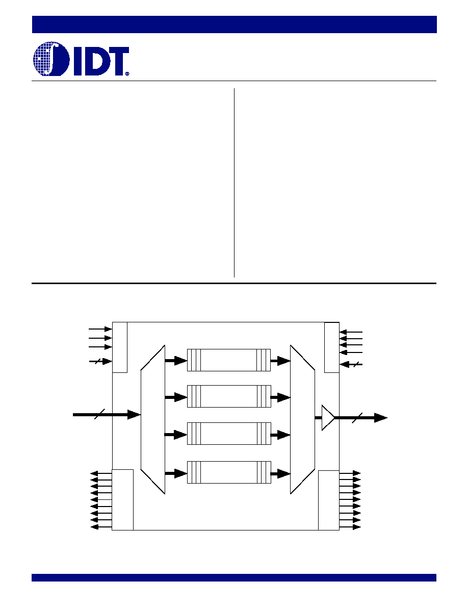
The multi-queue DDR flow-control device contains 4 Queues
each queue has a fixed size of:
IDT72T51248
-- 8,192 x 40 or 16,384 x 20 or 32,768 x 10
IDT72T51258
-- 16,384 x 40 or 32,768 x 20 or 65,536 x 10
IDT72T51268
-- 32,768 x 40 or 65,536 x 20 or 131,072 x 10
∑
∑
∑
∑
∑
Write to and Read from the same queue or different queues
simultaneously via totally independent ports
∑
∑
∑
∑
∑
Up to 200MHz operation of clocks
∑
∑
∑
∑
∑
Double Data Rate, DDR is selectable, providing up to 400Mbps
bandwidth per data pin
∑
∑
∑
∑
∑
User selectable Single or Double Data Rate modes on both the
write port and read port
∑
∑
∑
∑
∑
100% Bus Utilization, Read and Write on every clock cycle
∑
∑
∑
∑
∑
Global Bus Matching - All Queues have same Input bus width
and same Output bus width
∑
∑
∑
∑
∑
User Selectable Bus Matching options:
- x40in to x40out
- x40in to x20out
- x40in to x10out
- x20in to x40out
- x20in to x20out
- x20in to x10out
- x10in to x40out
- x10in to x20out
- x10in to x10out
∑
∑
∑
∑
∑
All I/O is LVTTL/ HSTL/ eHSTL user selectable
∑
∑
∑
∑
∑
3.3V tolerant inputs in LVTTL mode
FUNCTIONAL BLOCK DIAGRAM
∑
∑
∑
∑
∑
ERCLK &
EREN Echo outputs on read port
∑
∑
∑
∑
∑
Write Chip Select
WCS input for write port
∑
∑
∑
∑
∑
Read Chip Select
RCS input for read port
∑
∑
∑
∑
∑
User Selectable IDT Standard mode (using
EF and FF) or FWFT
mode (using
IR and OR)
∑
∑
∑
∑
∑
All 4 Queues have dedicated flag outputs
FF/IR, EF/OR, PAF
and
PAE
∑
∑
∑
∑
∑
A Composite Full/ Input Ready Flag gives status of the queue
selected on the write port
∑
∑
∑
∑
∑
A Composite Empty/ Output Ready flag gives status of the
queue selected on the read port
∑
∑
∑
∑
∑
Programmable Almost Empty and Almost Full flags per Queue
∑
∑
∑
∑
∑
Dedicated Serial Port for flag programming
∑
∑
∑
∑
∑
A Partial Reset is provided for each queue
∑
∑
∑
∑
∑
Power Down pin minimizes power consumption
∑
∑
∑
∑
∑
2.5V Supply Voltage
∑
∑
∑
∑
∑
Available in a 324-pin Plastic Ball Grid Array (PBGA)
19mm x 19mm, 1mm Pitch
∑
∑
∑
∑
∑
JTAG port provides boundary scan function and optional
programming mode
∑
∑
∑
∑
∑
Low Power, High Performance CMOS technology
∑
∑
∑
∑
∑
Industrial temperature range (-40
įį
įį
įC to +85įįįįįC)
Q[39:0]
x10,x20,x40
8,192 x 40
16,384 x40
32,768 x 40
8,192 x 40
16,384 x40
32,768 x 40
8,192 x 40
16,384 x40
32,768 x 40
8,192 x 40
16,384 x40
32,768 x 40
Data In
x10,x20,x40
Queue 0
Queue 1
Queue 2
Queue 3
D[39:0]
Data Out
EF0/OR0
PAE0
EF1/OR1
PAE1
EF2/OR2
PAE2
EF3/OR3
PAE3
CEF/COR
REN
RCS
RCLK
OE
Read Control
OS[1:0]
Read Port
Flag Outputs
6159 drw01
FF0/IR0
PAF0
FF1/IR1
PAF1
FF2/IR2
PAF2
FF3/IR3
PAF3
Write Port
Flag Outputs
CFF/CIR
WEN
WCS
WCLK
Write Control
IS[1:0]
MULTI-QUEUE DDR FLOW-CONTROL DEVICE
2
2

2
COMMERCIAL AND INDUSTRIAL
TEMPERATURE RANGES
IDT72T51248/72T51258/72T51268 2.5V MULTI-QUEUE DDR FLOW-CONTROL DEVICES
8,192 x 40 x 4, 16,384 x 40 x 4 and 32,768 x 40 x 4
DESCRIPTION
The multi-queue DDR flow-control devices are ideal for many applications
where functions such as data differentiation and parallel buffering of multiple data
paths are required. These applications may include communication and
networking systems such as routers, packet prioritization systems, data acqui-
sition systems, imaging systems and medical equipment.
The IDT72T51248/72T51258/72T51568 multi-queue DDR flow-control
devices are a single chip with four discrete FIFO queues available. All four
queues have a fixed density and based on the bus matching arrangement can
take the following memory arrangement: For the IDT72T51248, four queues
each queue being 8,192 x40 or 16,384 x20 or 32,768 x10. For the
IDT72T51258, four queues each queue being 16,384 x40 or 32,768 x20 or
65,536 x10. For the IDT72T51268, four queues each queue being 32,768 x40
or 65,536 x20 or 131,072 x10.
All queues within the device have a common data input bus (write port) and
a common data output bus (read port). Data written into the write port is directed
to a respective queue via an internal de-multiplex operation, the queue being
address by the user via a two bit input select bus. Data read from the read port
is accessed from a respective queue via an internal multiplex operation,
addressed by the user via a two bit output select bus. Data write and read
operations are totally independent of each other, a queue may be selected on
the write port and a different queue selected on the read port, or both ports may
select the same queue simultaneously.
Bus matching is provided on this device, the bus width selection is 'Global'
which means that all four queues will have a fixed input width and a fixed output
width. The write port bus width may be x10, x20 or x40 and the read port bus
width may be x10, x20 or x40. When bus matching is used the device ensures
the logical transfer of data throughput in a Little Endian manner.
As is typical with most IDT FIFO's, two types of data transfer are available,
IDT Standard mode and First word Fall Through (FWFT) Mode. This affects
the device operation and also the flag outputs. The device provides four
dedicated flag outputs for all internal Queue's. These flags are: Full/ Input Ready
flag, Empty/ Output Ready flag, Programmable Almost Empty flag and Program-
mable Almost Full. The programmable flags have default values, but can also
be set by the user to any point within the Queue depth. These programmable
flags can also be configured by the user for either Synchronous or Asynchro-
nous operation. The device also provides composite flags.
The multi-queue DDR device is capable of up to 200MHz operation on both
write clock and read clock inputs, these clocks being totally independent of each
other. Along with this high speed of operation the device ports are selectable
between Single Data Rate, SDR mode and Double Data Rate, DDR mode. If
Double Data Rate mode is selected data can be written into or read out of a
Queue on every rising and falling edge of a respective clock. For example, if
the write clock is running at 200MHz and the write port is set-up for DDR mode
a data input pin has a bandwidth of 400Mbps, so for a 40 bit wide bus a total
bandwidth of 16Gbps can be achieved.
The read port provides the user with a dedicated Echo Read Enable,
EREN
and Echo Read Clock,
ERCLK output. These outputs are helpful in higher speed
applications. Otherwise known as "Source Synchronous clocking" the echo
outputs provide tighter synchronization of the data transmitted from the multi-
queue flow-control device and the read clock being received at the down-
stream device.
A Master Reset input is provided and all set-up and configuration pins are
latched with respect to a Master Reset. For example, the bus width requirements
are selected at Master Reset. A Partial Reset is provided for each internal
Queue. When a Partial Reset is performed on a Queue, the read and write
pointers of that Queue only are reset to the first memory location. All other pointers
remain the same.
The device also has the capability of operating its I/O at either 2.5V LVTTL,
1.5V HSTL or 1.8V eHSTL levels. A Voltage Reference, V
REF
input is provided
for HSTL and eHSTL interfaces. The type of I/O is selected via the IOSEL pin.
The core supply voltage of the device, V
CC
is always 2.5V, however the output
pins have a separate supply, V
DDQ
which can be 2.5V, 1.8V or 1.5V. The device
also offers significant power savings in HSTL/eHSTL mode, most notably
achieved by the presence of a Power Down input,
PD.
A JTAG test port is provided. The multi-queue DDR device has a fully
functional Boundary Scan feature, compliant with IEEE 1149.1 Standard Test
Access Port and Boundary Scan Architecture. The JTAG port can also be used
to program the device set-up as described later in this document.
3
COMMERCIAL AND INDUSTRIAL
TEMPERATURE RANGES
IDT72T51248/72T51258/72T51268 2.5V MULTI-QUEUE DDR FLOW-CONTROL DEVICES
8,192 x 40 x 4, 16,384 x 40 x 4 and 32,768 x 40 x 4
INPUT
DEMUX
4 Identical
FIFO
Queues
1.3Mbit
Dual Port
Memory
x10, x20, x40
Write Control
Logic
WEN WCS
WCLK
Write Port
Flag Outputs
D0 - D39
Din
IS[1:0]
WDDR
2
FF0/IR0
PAF0
FF1/IR1
PAF1
FF2/IR2
PAF2
FF3/IR3
PAF3
CFF/CIR
Write Pointer
Bus
Configuration
IW[1:0]
OW[1:0]
2
2
HSTL I/O
Control
IOSEL
V
REF
OE
x10, x20, x40
Qout
OUTPUT
REGISTER
Q0 - Q39
6159 drw02
OUTPUT
MUX
MRS
Reset Logic
PRS0
PRS1
PRS2
PRS3
PD
SCLK
Flag Offset
Programming
SWEN
SREN
FWFT/SI
SDO
JTAG Control
(Boundary Scan)
TCK
TRST
TMS
TDI
TDO
RCLK
REN
Read Control
Logic
Read Pointer
RDDR
ERCLK
EREN
Read Port
Flag Outputs
and
Control Logic
2
EF0/OR0
PAE0
EF1/OR1
PAE1
EF2/OR2
PAE2
EF3/OR3
PAE3
CFF/COR
FSEL[1:0]
2
OS[1:0]
RCS
Figure 1. Multi-Queue DDR Flow-Control Device Block Diagram
4
COMMERCIAL AND INDUSTRIAL
TEMPERATURE RANGES
IDT72T51248/72T51258/72T51268 2.5V MULTI-QUEUE DDR FLOW-CONTROL DEVICES
8,192 x 40 x 4, 16,384 x 40 x 4 and 32,768 x 40 x 4
PRELIMINARY
A
B
C
D
E
F
G
H
J
K
L
M
N
P
R
T
V
CC
V
CC
GND
GND
V
CC
V
CC
V
CC
D39
Q33
Q36
FF2
PAF3
OS0
Q35
V
CC
V
CC
V
DDQ
V
CC
V
CC
V
CC
GND
V
DDQ
V
DDQ
V
DDQ
V
DDQ
D0
D1
D6
D3
D13
WCLK
GND
D38
V
CC
GND
GND
GND
GND
GND
GND
GND
GND
GND
GND
GND
GND
GND
GND
GND
GND
PRS0
PD
V
CC
GND
V
DDQ
V
CC
OE
PRS3
V
REF
MRS
D23
V
CC
V
CC
FWFT/SI
Q9
Q12
Q15
1
2
3
4
5
6
7
8
9
10
11
12
13
14
15
16
A1 BALL PAD CORNER
OW1
V
CC
D24
D27
D30
D33
D36
GND
V
DDQ
GND
GND
D26
D29
D32
D35
D7
D11
D14
D16
D18
D20
D25
D22
D28
D31
D34
D37
Q30
Q18
DNC
DNC
Q21
Q24
Q27
TDI
SREN
SCLK
D12
D15
D17
D19
D21
D4
D5
FSEL0
WDDR
D9
OW0
FSEL1
V
DDQ
IW0
GND
V
CC
TRST
IW1
TMS
TCK
GND
V
CC
V
CC
IOSEL
V
DDQ
GND
GND
V
CC
V
DDQ
V
DDQ
V
DDQ
V
DDQ
V
DDQ
V
DDQ
V
DDQ
V
DDQ
V
DDQ
V
DDQ
V
DDQ
V
DDQ
V
DDQ
V
DDQ
V
CC
V
CC
V
CC
V
CC
V
CC
V
CC
V
CC
V
CC
V
CC
V
CC
D2
SWEN
Q6
D10
RDDR
V
CC
PRS1
PRS2
D8
6159 drw03
U
V
IS1
GND
GND
V
CC
V
CC
Q38
GND
EF3
OS1
V
CC
GND
GND
V
CC
RCS
PAE3
V
CC
FF3
V
CC
REN
17
18
ERCLK
DNC
Q37
Q34
Q1
Q0
Q2
Q7
Q10
Q13
Q32
Q16
Q19
Q20
Q23
Q26
Q29
TDO
SDO
Q5
EREN
DNC
Q22
Q25
Q28
Q31
Q8
Q11
Q14
Q17
Q3
Q4
DNC
DNC
RCLK
Q39
V
CC
V
CC
V
CC
V
DDQ
V
CC
GND
V
CC
V
DDQ
V
DDQ
V
DDQ
GND
GND
V
CC
GND
GND
GND
GND
GND
V
DDQ
GND
GND
GND
V
CC
GND
GND
GND
GND
GND
V
DDQ
GND
GND
GND
GND
GND
GND
GND
V
CC
GND
GND
GND
GND
V
DDQ
GND
GND
GND
V
CC
GND
GND
GND
V
DDQ
GND
V
CC
V
CC
V
DDQ
V
CC
V
CC
GND
V
DDQ
V
DDQ
V
DDQ
GND
GND
V
CC
GND
GND
V
CC
GND
GND
V
CC
GND
GND
V
CC
GND
V
DDQ
GND
GND
V
DDQ
GND
GND
V
DDQ
GND
GND
V
DDQ
GND
V
CC
WEN
V
CC
WCS
V
CC
V
CC
IS0
PAE0
EF0
PAE1
FF1
PAE2
PAF0
EF1
CEF
EF2
FF0
PAF1
CFF
PAF2
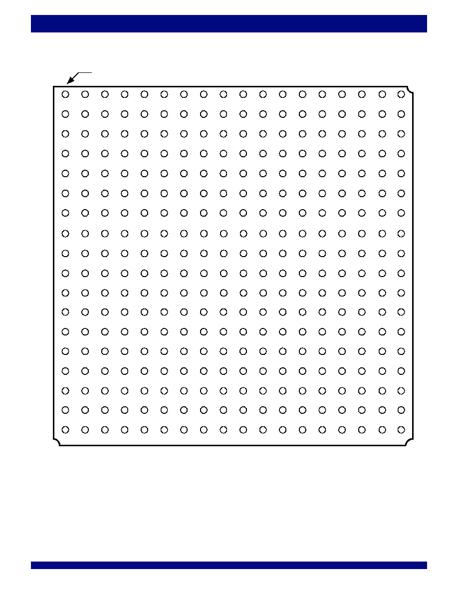
PBGA: 1mm Pin Pitch, 19mm x 19mm (BB324-1, order code: BB)
TOP VIEW
PIN CONFIGURATION
NOTE:
1. DNC - Do Not Connect.

5
COMMERCIAL AND INDUSTRIAL
TEMPERATURE RANGES
IDT72T51248/72T51258/72T51268 2.5V MULTI-QUEUE DDR FLOW-CONTROL DEVICES
8,192 x 40 x 4, 16,384 x 40 x 4 and 32,768 x 40 x 4
CEF/COR
Composite Empty/
HSTL-LVTTL This flag will represent the exact status of the current Queue being read without the user having to
Composite Output
OUTPUT
observe the correct Queue empty flag.
Ready Flag
CFF/CIR
Composite Full/
HSTL-LVTTL This flag will represent the exact status of the current Queue being written without the user having to
Composite Input
OUTPUT
observe the correct Queue full flag.
Ready flag
D[39:0]
Data Input Bus
LVTTL
These are the 40 data input pins. Data is written into the device via these input pins on the rising edge
Din
INPUT
of WCLK and/or the falling edge in DDR mode provided
WEN is LOW. Due to bus-matching not all
inputs may be used, any unused inputs should be tied to LOW.
EF0/OR0
Empty Flags 0/1/2/3 HSTL-LVTTL These are the Empty Flag (Standard IDT mode) or Output Ready Flag (FWFT mode) outputs for the
EF1/OR1,
or Output Ready
OUTPUT
read port of Queue 0, 1, 2 and 3 respectively.
EF2/OR2,
Flags 0/1/2/3
EF2/OR3
ERCLK
Echo Read Clock
HSTL-LVTTL This is the echo clock output for the read port. It is synchronous to the data output bus Q[35:0] and
OUTPUT
the input RCLK.
EREN
Echo Read Enable
HSTL-LVTTL This is the echo read enable output for the read port.
OUTPUT
Echo Read Enable is synchronous to the RCLK input and is active when a read operation has occurred
and a new word has been placed onto the data output bus.
FF0/IR0,
Full Flags 0/1/2/3
HSTL-LVTTL These are the Full Flag (Standard IDT mode) or Input Ready Flag (FWFT mode) outputs for the write
FF1/IR1,
or Input Ready
OUTPUT
port of Queue 0, 1, 2 and 3 respectively.
FF2/IR2,
Flags 0/1/2/3
FF3/IR3
FSEL
Flag Select
HSTL-LVTTL Flag select default offset pins. During Master reset, the FSEL pins are used to select one of 4 default
[1:0]
INPUT
PAE and PAF offsets. Both the PAE and the PAF offsets are programmed to the same value.
Values are: 00 = 7; 01 = 63; 10 = 127; 11 = 1023, meaning all four Queues have the same offset.
FWFT/SI
First Word Fall
HSTL-LVTTL During Master Reset, FWFT=1 selects First Word Fall Through mode, FWFT=0 selects IDT Standard
Through/ Serial
INPUT
mode. After Master Reset this pin is used for the Serial Data input for the programming of the
PAE and
Input
PAF flags offset registers.
IOSEL
I/O Select
CMOS
During Master Reset if the IOSEL pin is HIGH, then all inputs and outputs that are designated "LVTTL
INPUT
or HSTL" will be set to HSTL format. If LOW then they will be set to LVTTL format. All pins with a CMOS
format will remain unchanged. CMOS format means that the pin is intended to be tied to V
CC
or GND
and these particular pins are not tested for V
IL
or V
IH
.
IS[1:0]
Input Select
HSTL-LVTTL These inputs select one of the four Queue's to be written into on the write port. The address on the
INPUT
input select pins is set-up with respect to the WCLK.
IW[1:0]
Input Width
CMOS
This pin is used during Master Reset to select the input word width bus size for the device. 00 = x10;
INPUT
01 = x20; 10 = x40
MRS
Master Reset
HSTL-LVTTL This input provides a full device reset. All configuration pins are sampled based on a Master Reset
INPUT
operation.
OE
Output Enable
HSTL-LVTTL This is the Output Enable for the read port. The data outputs will be placed into High Impedance if
INPUT
this pin is HIGH. This input is asynchronous.
OS[1:0]
Output Select
HSTL-LVTTL These inputs select one of the four Queue's to be read from on the read port. The address on the
INPUT
output select pins is set-up with respect to the RCLK.
OW[1:0]
Output Width
CMOS
This pin is used during Master Reset to select the output word width bus size for the device. 00 = x10;
INPUT
01 = x20; 10 = x40
PAE0, PAE1
Programmable
HSTL-LVTTL These are the Programmable Almost Empty Flag outputs for the read port of Queue 0, 1, 2 and 3
PAE2, PAE3
Almost Empty
OUTPUT
respectively.
Flags 0/1/2/3
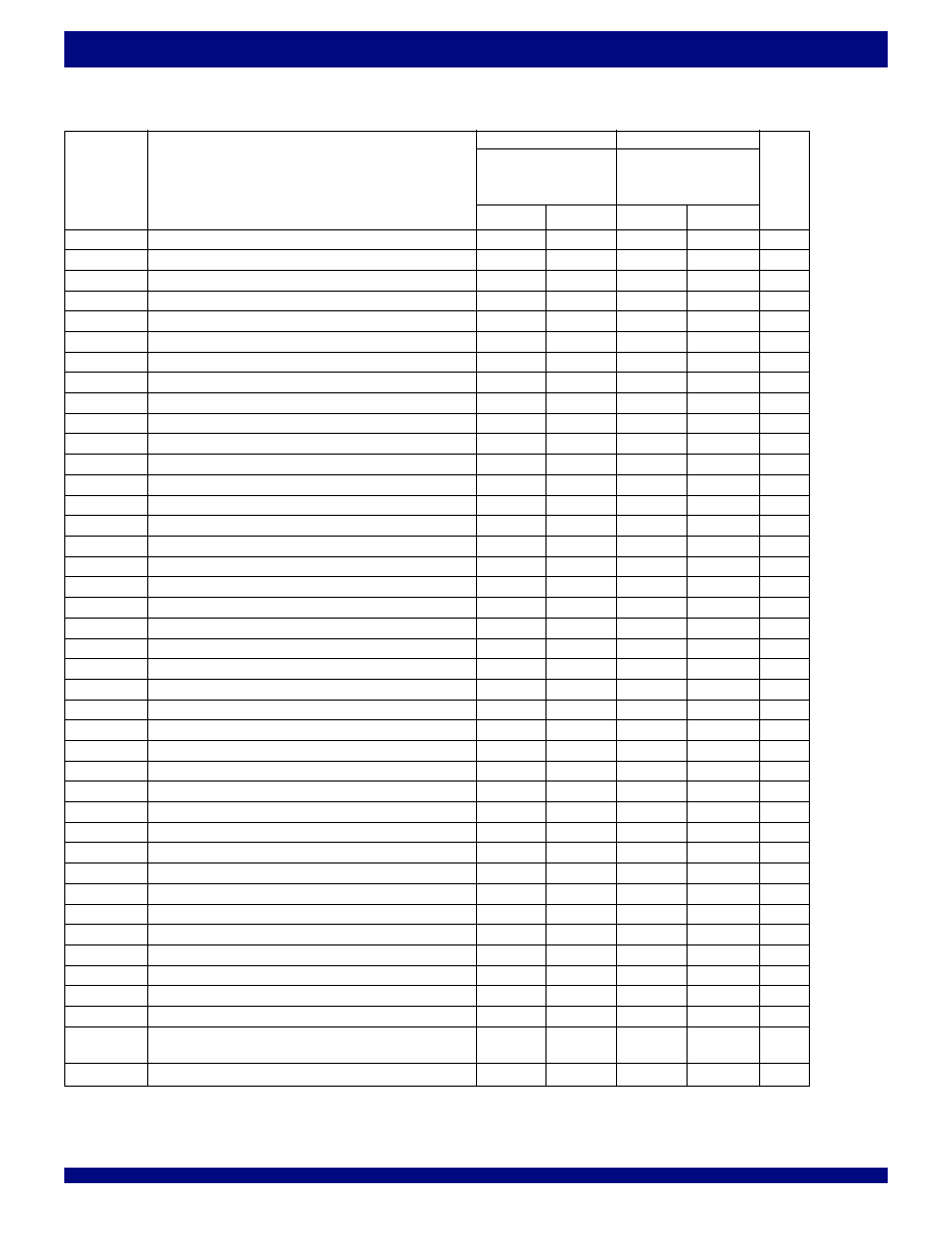
PIN DESCRIPTIONS
Symbol
Name
I/O TYPE
Description

6
COMMERCIAL AND INDUSTRIAL
TEMPERATURE RANGES
IDT72T51248/72T51258/72T51268 2.5V MULTI-QUEUE DDR FLOW-CONTROL DEVICES
8,192 x 40 x 4, 16,384 x 40 x 4 and 32,768 x 40 x 4
PAF0, PAF1
Programmable
HSTL-LVTTL These are the Programmable Almost Full Flag outputs for the write port of Queue 0, 1, 2 and 3
PAF2, PAF3
Almost Full
OUTPUT
respectively.
Flags 0/1/2/3
PD
Power Down
HSTL-LVTTL This input provides considerable power saving in HSTL/eHSTL mode. If this pin is low, the input
INPUT
level translators for all the data input pins, clocks and non-essential control pins are turned off. When
PD is brought high, a power-up sequence timing will have to be met before the inputs will be read.
It is essential that the user respects these conditions when powering down the part and powering up
the part, so as to not produce runt pulses or glitches on the clocks if the clocks are free running.
PRS0, PRS1
Partial
HSTL-LVTTL These are the Partial Reset inputs for each internal Queue. Resets the read and write and the flag
PRS2, PRS3
Reset 0/1/2/3
INPUT
pointers to zero, sets the output register to zero. During Partial Reset, the existing mode (IDT or FWFT)
and the programmable flag settings are all retained.
Q[39:0]
(2)
Data Output Bus
LVTTL
These are the 40 data output pins. Data is read out of the device via these output pins on the rising
OUTPUT
edge of RCLK provided that
REN is LOW, OE is LOW and the queue is selected. Due to bus-matching
not all outputs may be used, any unused outputs should not be connected.
RCLK
Read Clock
HSTL-LVTTL This is the clock input for the read port. All read port operations will be synchronous to this clock input.
INPUT
RCS
Read Chip Select
HSTL-LVTTL This is the read chip select input for the read port. All read operations will occur synchronous to the
INPUT
RCLK clock input provided that
REN and RCS are LOW. When RCS is HIGH the outputs are in high-
impedance and reads are disabled.
RDDR
Read Port DDR
CMOS
During master reset, this pin selects DDR or SDR format. If RDDR=1, then the RCLK reads a word
INPUT
on both the rising and falling edge of RCLK. If RDDR=0 then the RCLK reads a word only on the
rising edge of RCLK.
REN
Read Enable
HSTL-LVTTL This is the read enable input for the read port. All read operations will occur synchronous to the RCLK
INPUT
clock input provided that
REN and RCS are LOW.
SCLK
Serial Clock
HSTL-LVTTL Serial clock for programming and reading the
PAE and PAF offset registers. On the rising edge of each
INPUT
SCLK, when
SWEN is low, one bit of data is shifted into the PAE and PAF registers. On the rising edge
of each SCLK, when
SREN is low, one bit of data is shifted out of the readback PAE and PAF registers.
The reading of the
PAE and PAF registers is non-destructive.
SDO
Serial Data Output
HSTL-LVTTL When
SREN is brought low before the rising edge of SCLK, the contents of the PAE and PAF
OUTPUT
registers are copied to a readback serial register. While
SREN is maintained low, on each rising
edge of SCLK, one bit of data is shifted out of this readback register through the SDO output pin.
SREN
Serial Read Enable HSTL-LVTTL When
SREN is brought low before the rising edge of SCLK, the contents of the PAE and PAF
INPUT
registers are copied to a readback serial register. While
SREN is maintained low, on each rising
edge of SCLK, one bit of data is shifted out of this readback register through the SDO output pin.
SWEN
Serial Write Enable
HSTL-LVTTL On each rising edge of SCLK when
SWEN is low, data from the FWFT/SI pin is serially loaded
INPUT
into the
PAE and PAF registers. Each bit loaded into the registers go directly to the PAE/PAF
registers and the new flags will be in operation.
TCK
(3)
JTAG Clock
HSTL-LVTTL Clock input for JTAG function. One of four terminals required by IEEE Standard 1149.1-1990. Test
INPUT
operations of the device are synchronous to TCK. Data from TMS and TDI are sampled on the
rising edge of TCK and TDO change on the falling edge of TCK. If the JTAG function is not used
this signal needs to be tied to GND.
TDI
(3)
JTAG Test Data
HSTL-LVTTL One of four terminals required by IEEE Standard 1149.1-1990. During the JTAG boundary scan
Input
INPUT
operation, test data is serially scanned to the TDI on the rising edge of TCK to the Instruction
Register, ID Register, Bypass Register, or Boundary Scan chain. An internal pull-up resistor
forces TDI HIGH if left unconnected.
TDO
(3)
JTAG Test Data
HSTL-LVTTL One of four terminals required by IEEE Standard 1149.1-1990. During the JTAG boundary scan
Output
OUTPUT
operation, test data is serially loaded via the TDO on the falling edge of TCK from either the Instruction
Register, ID Register, Bypass Register and Boundary Scan chain. This output is high-impedance
except when shifting, while in SHIFT-DR and SHIFT-IR controller states.
PIN DESCRIPTIONS (CONTINUED)
Symbol
Name
I/O TYPE
Description

7
COMMERCIAL AND INDUSTRIAL
TEMPERATURE RANGES
IDT72T51248/72T51258/72T51268 2.5V MULTI-QUEUE DDR FLOW-CONTROL DEVICES
8,192 x 40 x 4, 16,384 x 40 x 4 and 32,768 x 40 x 4
TMS
(3)
JTAG Mode Select
HSTL-LVTTL TMS is a serial input pin. One of four terminals required by IEEE Standard 1149.1-1990. TMS directs
INPUT
the device through its TAP controller states sampled on the rising edge of TCK. An internal pull-up
resistor forces TMS HIGH if left unconnected.
TRST
(3)
JTAG Reset
HSTL-LVTTL
TRST is an asynchronous reset pin for the JTAG controller. The JTAG TAP controller is automatically
INPUT
reset upon power-up. If the TAP controller is not properly reset then the Queue outputs will always
be in high-impedance. If the JTAG function is used but the user does not want to use
TRST, then TRST
can be tied with
MRS to ensure proper Queue operation. If the JTAG function is not used then this
signal needs to be tied to GND. An internal pull-up resistor forces
TRST HIGH if left unconnected.
WCLK
Write Clock
HSTL-LVTTL This is the clock input for the write port. All write port operations will be synchronous to this clock input
INPUT
on either the rising edge (SDR mode) or rising or falling edge (DDR mode).
WCS
Write Chip Select
HSTL-LVTTL This is the write chip select input for the write port. All write operations will occur synchronous to the
INPUT
WCLK clock input provided that
WEN and WCS are LOW, sampled on WCLK.
WDDR
Write Port DDR
CMOS
During master reset, this pin selects DDR or SDR format. If WDDR=1, then the WCLK writes a word
INPUT
on both the rising and falling edge. If WDDR=0 then the WCLK writes a word only on the rising edge.
WEN
Write Enable
HSTL-LVTTL This is the write enable input for the write port. All write operations will occur synchronous to the WCLK
INPUT
clock input provided that
WEN and WCS are LOW, sampled on the rising edge of WCLK.
V
CC
+2.5 Supply
PWR
Power supply for the chip core, 2.5V.
V
DDQ
Output Rail Voltage
PWR
Power supply for all of the chip's outputs. 2.5V for LVTTL outputs, 1.5V for HSTL outputs or 1.8V for
eHSTL outputs.
GND
Ground Pin
GND
Ground connection.
V
REF
Reference voltage
Analog
Voltage Reference input for HSTL inputs.
PIN DESCRIPTIONS (CONTINUED)
Symbol
Name
I/O TYPE
Description
NOTES:
1. All CMOS pins should remain unchanged. CMOS format means that the pin is intended to be tied directly to V
CC
or GND and these particular pins are not tested for V
IH
or V
IL
.
2. All unused outputs should be left un-connected.
3. These pins are for the JTAG port. Please refer to pages 28-31, Figure 4-6 for JTAG information.

8
COMMERCIAL AND INDUSTRIAL
TEMPERATURE RANGES
IDT72T51248/72T51258/72T51268 2.5V MULTI-QUEUE DDR FLOW-CONTROL DEVICES
8,192 x 40 x 4, 16,384 x 40 x 4 and 32,768 x 40 x 4
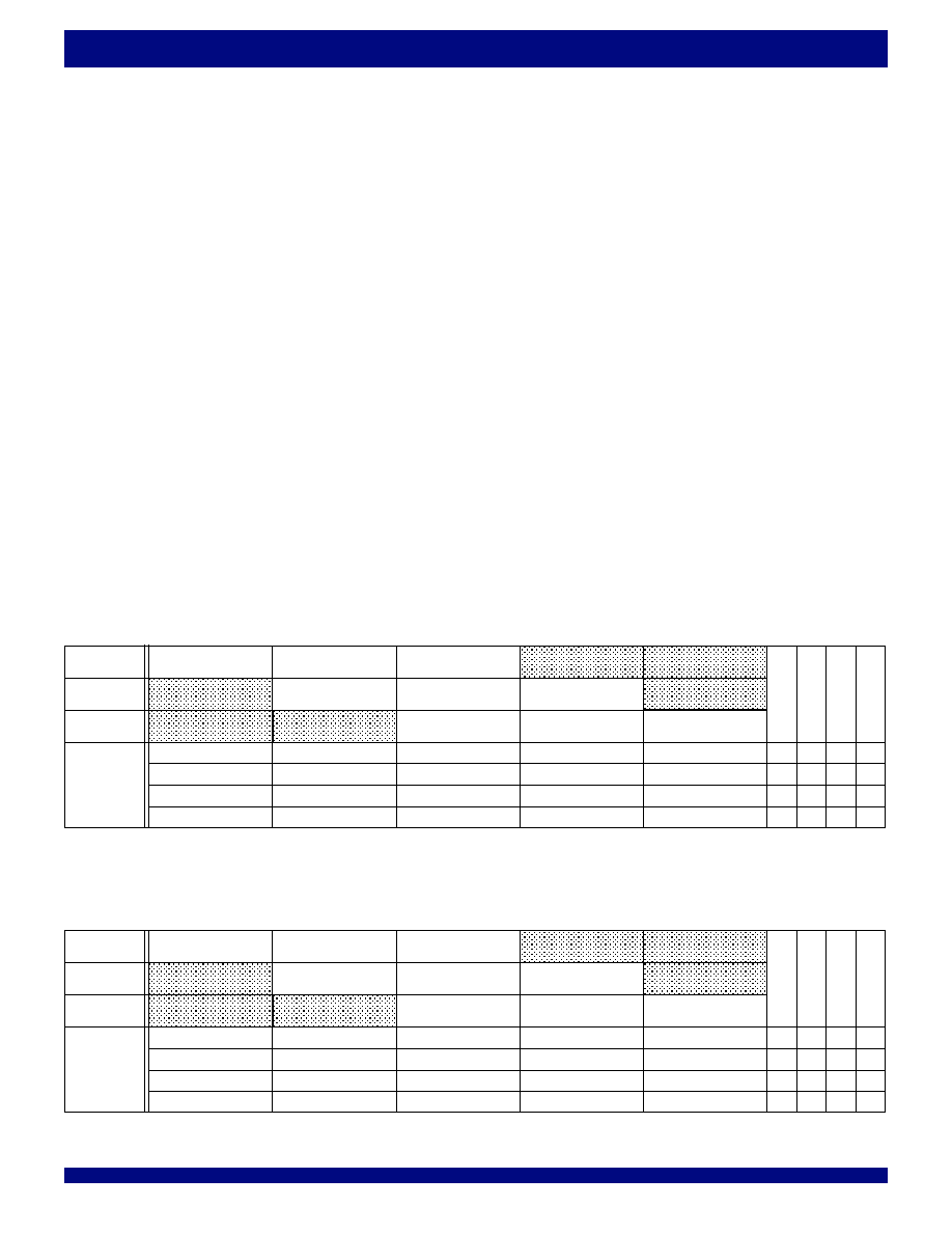
ABSOLUTE MAXIMUM RATINGS
NOTES:
1. Stresses greater than those listed under ABSOLUTE MAXIMUM RATINGS may cause
permanent damage to the device. This is a stress rating only and functional operation
of the device at these or any other conditions above those indicated in the operational
sections of this specification is not implied. Exposure to absolute maximum rating
conditions for extended periods may affect reliability.
2. Compliant with JEDEC JESD8-5. V
CC
terminal only.
Symbol
Parameter
(1)
Conditions
Max.
Unit
C
IN
(2,3)
Input
V
IN
= 0V
10
(3)
pF
Capacitance
C
OUT
(1,2)
Output
V
OUT
= 0V
10
pF
Capacitance
CAPACITANCE
(T
A
= +25
įC, f = 1.0MHz)
NOTES:
1. With output deselected, (
OE
V
IH
).
2. Characterized values, not currently tested.
3. C
IN
for Vref is 20pF.
Symbol
Parameter
Min.
Typ.
Max.
Unit
V
CC
Supply Voltage with reference to GND
2.375
2.5
2.625
V
V
DDQ
Output Supply Voltage
LVTTL
2.375
2.5
2.625
V
eHSTL
1.7
1.8
1.9
V
HSTL
(2)
1.4
1.5
1.6
V
V
REF
Voltage Reference Input
eHSTL
0.8
0.9
1.0
V
HSTL
(2)
0.68
0.75
0.9
V
V
IH
Input High Voltage
LVTTL
1.7
--
3.45
V
eHSTL
V
REF
+0.1
--
V
DDQ
+0.3
V
HSTL
(2)
V
REF
+0.1
--
V
DDQ
+0.3
V
V
IL
Input Low Voltage
LVTTL
--
--
0.7
V
eHSTL
-0.3
--
V
REF
-0.1
V
HSTL
(2)
-0.3
--
V
REF
-0.1
V
T
A
Operating Temperature Commercial
0
--
+70
į
C
T
A
Operating Temperature Industrial
-40
--
+85
į
C
RECOMMENDED DC OPERATING CONDITIONS
NOTES:
1. V
REF
is only required for HSTL or eHSTL inputs. V
REF
should be tied LOW for LVTTL operation.
2. Compliant with JEDEC JESD8-6.
3. GND = Ground.
Symbol
Rating
Com'l & Ind'l
Unit
V
TERM
Terminal Voltage
≠0.5 to +3.6
(2)
V
with respect to GND
T
STG
Storage Temperature
≠55 to +125
į
C
I
OUT
DC Output Current
≠50 to +50
mA

9
COMMERCIAL AND INDUSTRIAL
TEMPERATURE RANGES
IDT72T51248/72T51258/72T51268 2.5V MULTI-QUEUE DDR FLOW-CONTROL DEVICES
8,192 x 40 x 4, 16,384 x 40 x 4 and 32,768 x 40 x 4
DC ELECTRICAL CHARACTERISTICS
(Industrial: V
CC
= 2.5V Ī 0.125V, T
A
= -40
įC to +85įC)
Symbol
Parameter
Min.
Max.
Unit
I
LI
Input Leakage Current
≠10
+10
ĶA
I
LO
Output Leakage Current
≠10
+10
ĶA
V
OH
(7)
Output Logic "1" Voltage,
I
OH
= ≠8 mA @LVTTL
V
DDQ
-0.4
--
V
I
OH
= ≠8 mA @eHSTL
V
DDQ
-0.4
--
V
I
OH
= ≠8 mA @HSTL
V
DDQ
-0.4
--
V
V
OL
Output Logic "0" Voltage,
I
OL
= 8 mA @LVTTL
--
0.4
V
I
OL
= 8 mA @eHSTL
--
0.4
V
I
OL
= 8 mA @HSTL
--
0.4
V
I
CC1
(1,2,3)
Active V
CC
Current
-- LVTTL
--
144
mA
(See Note 8 for test conditions)
-- eHSTL
--
234
mA
-- HSTL
--
231
mA
I
CC3
(1,2,3)
Standby V
CC
Current
-- LVTTL
--
82
mA
(See Note 9 for test conditions)
-- eHSTL
--
163
mA
-- HSTL
--
159
mA
I
CC5
(1,2,3)
Power Down V
CC
Current
-- LVTTL
--
8
mA
(See Note 10 for test conditions)
-- eHSTL
--
25
mA
-- HSTL
--
24
mA
NOTES:
1. Both WCLK and RCLK toggling at 20MHz.
2. Data inputs toggling at 10MHz.
3. Typical I
CC1
calculation
:
for LVTTL I/O I
CC1
(mA) =
6 x fs
, fs = WCLK frequency = RCLK frequency (in MHz)
for HSTL or eHSTL I/O I
CC1
(mA) =
90+ (6 x fs)
, fs = WCLK frequency = RCLK frequency (in MHz)
4. Typical I
DDQ
calculation: With Data Outputs in High-Impedance: I
DDQ
(mA) =
0.25 x fs, fs = WCLK = RCLK frequency (in MHz)
With Data Outputs in Low-Impedance: I
DDQ
(mA) =
(C
L
x V
DDQ
x fs x N) /2000
fs = WCLK frequency = RCLK frequency (in MHz), V
DDQ
= 2.5V for LVTTL; 1.5V for HSTL; 1.8V for eHSTL
t
A
= 25įC, C
L
= capacitive load (pf), N = Number of bits switching
5. Total Power consumed: PT = [(V
CC
x I
CC
) + (V
DDQ
x I
DDQ
)]. I
OH
= -8mA for all voltage levels.
6. I
OH
8mA, I
OL
-8mA.
7. Outputs are not 3.3V tolerant.
8. V
CC
= 2.5V, WCLK = RCLK = 20MHz,
WEN = REN = LOW, WCS = RCS = LOW, OE = LOW, PD = HIGH.
9. V
CC
= 2.5V, WCLK = RCLK = 20MHz,
WEN = REN = HIGH, WCS = RCS = HIGH, OE = LOW, PD = HIGH.
10. V
CC
= 2.5V, WCLK = RCLK = 20MHz,
WEN = REN = HIGH, WCS = RCS = HIGH, OE = LOW, PD = LOW.
10
COMMERCIAL AND INDUSTRIAL
TEMPERATURE RANGES
IDT72T51248/72T51258/72T51268 2.5V MULTI-QUEUE DDR FLOW-CONTROL DEVICES
8,192 x 40 x 4, 16,384 x 40 x 4 and 32,768 x 40 x 4
P R E L I M I N A R
Y
AC ELECTRICAL CHARACTERISTICS
(1)
(Commercial: V
CC
= 2.5V Ī 0.15V, T
A
= 0
įC to +70įC;Industrial: V
CC
= 2.5V Ī 0.15V, T
A
= -40
įC to +85įC; JEDEC compliant)
Commercial & Industrial
Commercial & Industrial
IDT72T51248L5
IDT72T51248L6-7
IDT72T51258L5
IDT72T51258L6-7
IDT72T51268L5
IDT72T51268L6-7
Symbol
Parameter
Min.
Max.
Min.
Max.
Unit
f
S
Clock Cycle Frequency (WCLK & RCLK)
--
200
--
150
MHz
t
A
Data Access Time
0.6
3.6
0.6
3.8
ns
t
CLK
Clock Cycle Time
5
--
6.7
--
ns
t
CLKH
Clock High Time
2.3
--
2.8
--
ns
t
CLKL
Clock Low Time
2.3
--
2.8
--
ns
t
DS
Data Setup Time
1.5
--
2.0
--
ns
t
DH
Data Hold Time
0.5
--
0.5
--
ns
t
ENS
Enable Setup Time
1.5
--
2.0
--
ns
t
ENH
Enable Hold Time
0.5
--
0.5
--
ns
f
C
Clock Cycle Frequency (SCLK)
--
10
--
10
MHz
t
ASO
Serial Output Data Access Time
--
20
--
20
ns
t
SCLK
Serial Clock Cycle
100
--
100
--
ns
t
SCKH
Serial Clock High
45
--
45
--
ns
t
SCKL
Serial Clock Low
45
--
45
--
ns
t
SDS
Serial Data In Setup
15
--
15
--
ns
t
SDH
Serial Data In Hold
5
--
5
--
ns
t
SENS
Serial Enable Setup
5
--
5
--
ns
t
SENH
Serial Enable Hold
5
--
5
--
ns
t
RS
Reset Pulse Width
200
--
200
--
ns
t
RSS
Reset Setup Time
15
--
15
--
ns
t
RSR
Reset Recovery Time
10
--
10
--
ns
t
RSF
Reset to Flag and Output Time
--
12
--
15
ns
t
OLZ
(OE -
Q
n)
(2)
Output Enable to Output in Low-Impedance
0.6
3.6
0.8
3.8
ns
t
OHZ
(2)
Output Enable to Output in High-Impedance
0.6
3.6
0.8
3.8
ns
t
OE
Output Enable to Data Output Valid
0.6
3.6
0.8
3.8
ns
t
WFF
Write Clock to
FF or IR
--
3.6
--
3.8
ns
t
REF
Read Clock to
EF or OR
--
3.6
--
3.8
ns
t
CEF
Read Clock to Composite
EF or OR
--
3.6
--
3.8
ns
t
CFF
Write Clock to Composite
FF or IR
--
3.6
--
3.8
ns
t
PAFS
Write Clock to Synchronous Programmable Almost-Full Flag
--
3.6
--
3.8
ns
t
PAES
Read Clock to Synchronous Programmable Almost-Empty Flag
--
3.6
--
3.8
ns
t
PAFA
Write Clock to Asynchronous Programmable Almost-Full Flag
--
10
--
12
ns
t
PAEA
Read Clock to Asynchronous Programmable Almost-Empty Flag
--
10
--
12
ns
t
ERCLK
RCLK to Echo RCLK Output
--
4.0
--
4.3
ns
t
CLKEN
RCLK to Echo
REN Output
--
3.6
--
3.8
ns
t
D
Time Between Data Switching and ERCLK edge
0.4
--
0.5
--
ns
t
RCSLZ
RCLK to Active from High-Impedance
--
3.6
--
3.8
ns
t
RCSHZ
RCLK to High-Impedance
--
3.6
--
3.8
ns
t
SKEW1
SKEW
time between RCLK and WCLK for
EF/OR and FF/IR
4
--
5
--
ns
t
SKEW2
SKEW
time between RCLK and WCLK for
EF/OR and FF/IR in
5
--
7
--
ns
DDR mode
t
SKEW3
SKEW
time between RCLK and WCLK for
PAE and PAF
5
--
7
--
ns
NOTES:
1. This applies to both DDR and SDR modes of operation.
2. Values guaranteed by design, not currently tested.
11
COMMERCIAL AND INDUSTRIAL
TEMPERATURE RANGES
IDT72T51248/72T51258/72T51268 2.5V MULTI-QUEUE DDR FLOW-CONTROL DEVICES
8,192 x 40 x 4, 16,384 x 40 x 4 and 32,768 x 40 x 4
AC TEST LOADS
Figure 2a. AC Test Load
6159 drw04
50
V
DDQ
/2
I/O
Z
0
= 50
Input Pulse Levels
0.25 to 1.25V
Input Rise/Fall Times
0.4ns
Input Timing Reference Levels
0.75
Output Reference Levels
V
DDQ
/2
HSTL
1.5V AC TEST CONDITIONS
Input Pulse Levels
GND to 2.5V
Input Rise/Fall Times
1ns
Input Timing Reference Levels
V
CC
/2
Output Reference Levels
V
DDQ
/2
LVTTL
2.5V AC TEST CONDITIONS
NOTE:
1. V
DDQ
= 1.5V.
NOTE:
1. For LVTTL, V
CC
= V
DDQ
= 2.5V.
Input Pulse Levels
0.4 to 1.4V
Input Rise/Fall Times
0.4ns
Input Timing Reference Levels
0.9
Output Reference Levels
V
DDQ
/2
EXTENDED HSTL
1.8V AC TEST CONDITIONS
NOTE:
1. V
DDQ
= 1.8V.
Figure 2b. Lumped Capacitive Load, Typical Derating
6159 drw04a
6
5
4
3
2
1
20 30 50
80 100
200
Capacitance (pF)
t
CD
(Typical, ns)
12
COMMERCIAL AND INDUSTRIAL
TEMPERATURE RANGES
IDT72T51248/72T51258/72T51268 2.5V MULTI-QUEUE DDR FLOW-CONTROL DEVICES
8,192 x 40 x 4, 16,384 x 40 x 4 and 32,768 x 40 x 4
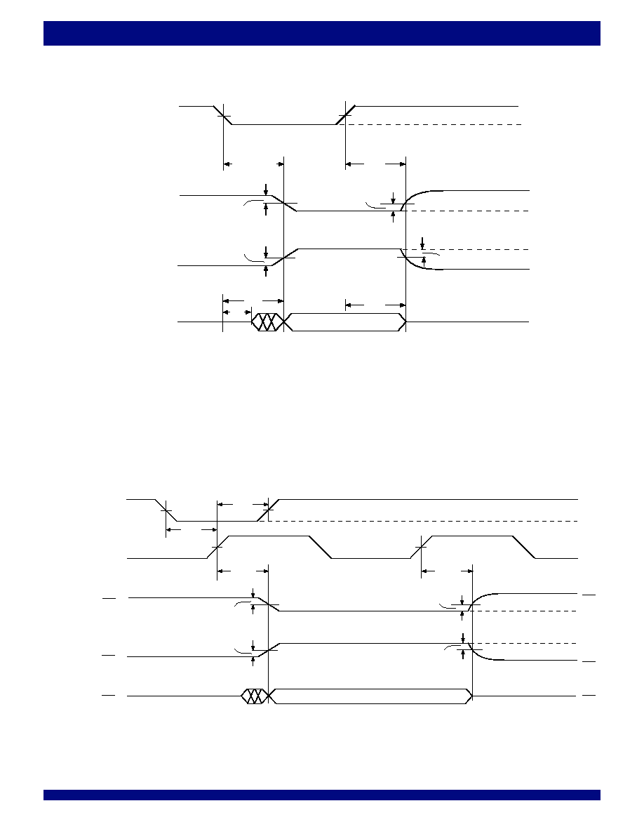
OUTPUT ENABLE & DISABLE TIMING
V
IH
OE
V
IL
t
OE &
t
OLZ
100mV
100mV
t
OHZ
100mV
100mV
Single Output
Normally
LOW
Single Output
Normally
HIGH
V
OL
V
OH
V
DDQ
/2
6159 drw05
Output
Enable
Output
Disable
V
DDQ
/2
V
DDQ
/2
V
DDQ
/2
t
OLZ
Current data in output register
t
OE
V
DDQ
/2
Output Bus
V
DDQ
/2
t
OHZ
READ CHIP SELECT ENABLE & DISABLE TIMING
NOTES:
1.
REN is HIGH.
2.
OE is LOW.
V
IH
RCS
V
IL
t
ENS
t
ENH
t
RCSLZ
RCLK
V
DDQ
2
V
DDQ
2
100mV
100mV
t
RCSHZ
100mV
100mV
Single Output
Normally
LOW
Single Output
Normally
HIGH
V
OL
V
OH
V
DDQ
2
V
DDQ
2
6158 drw06
Output Bus
Current data in output register
V
DDQ
2
V
DDQ
2
NOTES:
1.
REN is HIGH.
2.
RCS is LOW.

13
COMMERCIAL AND INDUSTRIAL
TEMPERATURE RANGES
IDT72T51248/72T51258/72T51268 2.5V MULTI-QUEUE DDR FLOW-CONTROL DEVICES
8,192 x 40 x 4, 16,384 x 40 x 4 and 32,768 x 40 x 4
FUNCTIONAL DESCRIPTION
MASTER RESET & DEVICE CONFIGURATION -
MRS
During Master Reset the device configuration and settings are determined,
this includes the following:
1. IDT Standard or First Word Fall Through (FWFT) flag timing mode
2. Single or Double Data Rates on both the Write and Read ports
3. Programmable flag mode, synchronous or asynchronous timing
4. Write and Read Port Bus Widths, x40, x20, or x10
5. Default Offsets for the programmable flags, 7, 63, 127, or 1023
6. LVTTL or HSTL I/O selection
7. Default starting Queue
The state of the configuration inputs during master reset will determine which
of the above modes are selected. A master reset comprises of pulsing the
MRS
input pin from high to low for a period of time (t
RS
) with the configuration inputs
held in their respective states. Table 1 summarizes the configuration modes
available during master reset. They are described as follows:
IDT Standard or FWFT Mode. The two available flag timing modes are
selected using the FWFT/SI input. If FWFT/SI is LOW during master reset then
IDT Standard mode is selected, if it is high then FWFT mode is selected. The
timing modes are described later in Timing Modes: IDT Standard vs First Word
Fall Through (FWFT) Mode section.
Single Data Rate (SDR) or Double Data Rate (DDR). The input/output
data rates are port selectable. This is a versatile feature that allows the user to
select either SDR or DDR on the write ports and/or reads ports of all Queues
using the WDDR and/or RDDR inputs. If WDDR is LOW during master reset
then the write ports of all Queues will function in SDR mode, if it is high then the
write ports will be DDR mode. If RDDR is LOW during master reset then the read
ports of all Queues will function in SDR mode, if it is high then the read port will
be DDR mode. This feature is described in the Signal Descriptions section.
Programmable Almost Empty/Full Flags. The almost empty and almost
full offsets are user programmable, with offset values listed in Table 2. Both
PAE
and
PAF are double-buffered and updated based on the rising edge of their
respective clocks.
PAE with respect to RCLK and PAF with respect to WCLK.
Selectable Bus Width. The bus width can be selected on independently
the read and write ports using the IW and OW inputs. IW pins set the write port
width to x40, x20 or x10 bits wide. The OW pins set the read port to x40, x20
or x10 bits wide.
Programmable Flag Offset Values. These offset values can be user
programmed or they can be set to one of four default values during a master
reset. For default programming, the state of the FSEL[1:0] inputs during master
reset will determine the value. Table 2, Default Programmable offsets lists the
four offset values and how to select them. For programming the offset values to
a specific number, use the serial programming signals (SCLK,
SWEN, SREN,
FWFT/SI) to load the value into the offset register. You may also use the JTAG
port on this device to load the offset value. Keep in mind that you must disable
the serial programming signals if you plan to use the JTAG port for loading the
offset values. To disable the serial programming signals, tie SCLK,
SWEN,
SREN, and FWFT/SI to V
CC
. A thorough explanation of the serial and JTAG
programming of the flag offset values is provided in the next section titled "Serial
Write and Reading of Offset Registers".
I/O Level Selection. The I/Os can be selected for either 2.5V LVTTL levels
or 1.5V HSTL / 1.8V eHSTL levels. The state of the IOSEL input will determine
which I/O level will be selected. If IOSEL is HIGH then the applicable I/Os will
be 1.5V HSTL or 1.8V eHSTL, depending on the voltage level applied to V
DDQ
and V
REF
. For HSTL, V
DDQ
= 1.5V and V
REF
= Ĺ V
DDQ.
For eHSTL V
DDQ
= 1.8V and V
REF
= Ĺ V
DDQ
. If IOSEL is LOW then the applicable I/Os will be
2.5V LVTTL. As noted in the Pin Description section, IOSEL is a CMOS input
and must be tied to either V
CC
or GND for proper operation.
Input and Output Selection. During master reset, the value of IS[1:0]
and OS[1:0] will be held constant and indicates which internal Queue the read
and write port will select for initial operation. Data will be written to or read from
this internal Queue on the first valid write and read operation after master reset.
IDT72T51248 / IDT72T51258 / IDT72T51268
FSEL1
FSEL0
Offsets n,m
0
0
7
0
1
63
1
0
127
1
1
1023
TABLE 2 -- DEFAULT PROGRAMMABLE
FLAG OFFSETS
NOTES:
1. In default programming, the offset value selected applies to all internal Queues.
2. To program different offset values for each Queue, serial programming must be used.
TABLE 1 -- DEVICE CONFIGURATION
PINS
VALUES
CONFIGURATION
FWFT/SI
0
IDT Standard
1
FWFT
WDDR
0
Single Data Rate write port
1
Double Data Rate write port
RDDR
0
Single Data Rate read port
1
Double Data Rate read port
IW[1:0]
00
Write port is 10 bits wide
01
Write port is 20 bits wide
10
Write port is 40 bits wide
11
Restricted
OW[1:0]
00
Read port is 10 bits wide
01
Read port is 20 bits wide
10
Read port is 40 bits wide
11
Restricted
FSEL[1:0]
00
Programmable flag offset registers value = 7
01
Programmable flag offset registers value = 63
10
Programmable flag offset registers value = 127
11
Programmable flag offset registers value = 1023
IOSEL
0
All applicable I/Os (except CMOS) are LVTTL
1
All applicable I/Os (except CMOS) are HSTL/eHSTL
IS[1:0]
00
Queue0
01
Queue1
10
Queue2
11
Queue3
OS[1:0]
00
Queue0
01
Queue1
10
Queue2
11
Queue3

14
COMMERCIAL AND INDUSTRIAL
TEMPERATURE RANGES
IDT72T51248/72T51258/72T51268 2.5V MULTI-QUEUE DDR FLOW-CONTROL DEVICES
8,192 x 40 x 4, 16,384 x 40 x 4 and 32,768 x 40 x 4
6159 drw08
Offset
Register
PAE3
PAF3
PAE2
PAF2
PAE1
PAF1
PAE0
PAF0
14 - 26
27 - 39
40 - 52
53 - 65
66 - 78
1 - 13
79 - 91
92 - 104
Serial Bits
IDT72T51248
IW/OW = x20
or
IDT72T51258
IW/OW = x40
IDT72T51248
IW/OW = x20
or IDT72T51258
IW/OW = x20
or IDT72T51268
IW/OW = x40
IDT72T51248
IW/OW = x40
IDT72T51268
IW/OW = x10
IDT72T51258
IW/OW = x10
or
IDT72T51268
IW/OW = x20
15 - 28
29 - 42
43 - 56
57 - 70
71 - 84
1 - 14
85 - 98
99 - 112
16 - 30
31 - 45
46 - 60
61 - 75
76 - 90
1 - 15
91 - 105
106 - 120
17 - 32
33 - 48
49 - 64
65 - 80
81 - 96
1 - 16
97 - 112
113 - 128
18 - 34
35 - 51
52 - 68
69 - 85
86 - 102
1 - 17
103 - 119
120 - 136
Figure 4. Offset Registers Serial Bit Sequence
SCLK
TDI*
0008
TCK*
SWEN
0
SREN
1
No Operation
IW/OW = x40
Serial read from registers:
104 bits for the IDT72T51248
112 bits for the IDT72T51258
120 bits for the IDT72T51268
1 bit for each rising SCLK edge
starting with empty offset (LSB)
ending with full offset (MSB)
IDT72T51248
IDT72T51258
IDT72T51268
Serial write into register:
104 bits for the IDT72T51248
112 bits for the IDT72T51258
120 bits for the IDT72T51268
1 bit for each rising SCLK edge
starting with empty offset (LSB)
ending with full offset (MSB)
6159 drw07
IW/OW = x20
Serial write into register:
112 bits for the IDT72T51248
120 bits for the IDT72T51258
128 bits for the IDT72T51268
1 bit for each rising SCLK edge
starting with empty offset (LSB)
ending with full offset (MSB)
0007
1
1
Serial read from registers:
112 bits for the IDT72T51248
120 bits for the IDT72T51258
128 bits for the IDT72T51268
1 bit for each rising SCLK edge
starting with empty offset (LSB)
ending with full offset (MSB)
No Operation
Don't
care
except
0008 &
0007
1
0
X
X
IW/OW = x10
Serial write into register:
120 bits for the IDT72T51248
128 bits for the IDT72T51258
136 bits for the IDT72T51268
1 bit for each rising SCLK edge
starting with empty offset (LSB)
ending with full offset (MSB)
Serial read from registers:
120 bits for the IDT72T51248
128 bits for the IDT72T51258
136 bits for the IDT72T51268
1 bit for each rising SCLK edge
starting with empty offset (LSB)
ending with full offset (MSB)
No Operation
NOTES:
* Programming done using the JTAG port.
1. The programming methods apply to both IDT Standard mode and FWFT mode.
2. Parallel programming is not featured in this device.
3. The number of bits includes programming to all four dedicated
PAE/PAF offset registers.
Figure 3. Programmable Flag Offset Programming Methods
15
COMMERCIAL AND INDUSTRIAL
TEMPERATURE RANGES
IDT72T51248/72T51258/72T51268 2.5V MULTI-QUEUE DDR FLOW-CONTROL DEVICES
8,192 x 40 x 4, 16,384 x 40 x 4 and 32,768 x 40 x 4
6159 drw09
TABLE 4
STATUS FLAGS FOR FWFT MODE
TABLE 3
STATUS FLAGS FOR IDT STANDARD MODE
0
1 to n
(1)
(n+1) to (8,192 - m)
8,192
FF PAF PAE EF
H
H
L
L
H
H
L
H
H
L
H
H
L
L
H
H
IDT72T51248
IDT72T51258
IDT72T51258
IDT72T51248
IDT72T51248
OW = x20
Number of
Words in
Queue
OW = x10
IDT72T51268
OW = x40
IDT72T51268
IDT72T51258
IDT72T51268
0
1 to n
(1)
(n+1) to (16,384 - m)
16,384
0
1 to n
(1)
(n+1) to (32,768 - m)
32,768
0
1 to n
(1)
(n+1) to (65,536 - m)
65,536
0
1 to n
(1)
(n+1) to (131,072 - m)
131,072
0
1 to n+1
(1)
(n+2) to (8,193 - m)
8,193
FF PAF PAE EF
H
H
L
L
H
H
L
H
H
L
H
H
L
L
H
H
IDT72T51248
IDT72T51258
IDT72T51258
IDT72T51248
IDT72T51248
OW = x20
Number of
Words in
Queue
OW = x10
IDT72T51268
OW = x40
IDT72T51268
IDT72T51258
IDT72T51268
0
1 to n+1
(1)
(n+2) to (16,385 - m)
16,385
0
1 to n+1
(1)
(n+2) to (32,769 - m)
32,769
0
1 to n+1
(1)
(n+2) to (65,537 - m)
65,537
0
1 to n+1
(1)
(n+2) to (131,073 - m)
131,073
TIMING MODES: IDT STANDARD vs FIRST WORD FALL THROUGH
(FWFT) MODE
The IDT72T51248/72T51258/72T51268 support two different timing modes
of operation: IDT Standard mode or First Word Fall Through (FWFT) mode.
The selection of which mode will operate is determined during master reset,
by the state of the FWFT input.
During master reset, if the FWFT pin is LOW, then IDT Standard mode will
be selected. This mode uses the Empty Flag (
EF) to indicate whether or not
there are any words present in the Queue. It also uses the Full Flag (
FF) to
indicate whether or not the Queue has any free space for writing. In IDT
Standard mode, every word read from the Queue, including the first, must be
requested using the Read Enable (
REN) and RCLK.
If the FWFT pin is HIGH during master reset, then FWFT mode will be
selected. This mode uses Output Ready (
OR) to indicate whether or not there
is valid data at the data outputs. It also uses Input Ready (
IR) to indicate whether
or not the Queue has any free space for writing. In the FWFT mode, the first
word written to an empty Queue goes directly to output bus after three RCLK
rising edges, applying
RCS = LOW is not necessary. However, subsequent
words must be accessed using the
RCS and RCLK. Various signals, in both
inputs and outputs operate differently depending on which timing mode is in
effect. The timing mode selected affects all internal Queues equally.
IDT STANDARD MODE
In this mode, the status flags
FF, PAF, PAE, and EF operate in the manner
outlined in Table 3. To write data into the Queue, Write Enable (
WEN) and write
chip select
WCS must be LOW. Data presented to the D[39:0] lines will be
clocked into the Queue on subsequent transitions of the Write Clock (WCLK).
After the first write is performed, the Empty Flag (
EF) will go HIGH after three
clock cycles. Subsequent writes will continue to fill up the Queue. The
Programmable Almost-Empty flag (
PAE) will go HIGH after n + 1 words have
been loaded into the Queue, where n is the empty offset value. The default
setting for these values are listed in Table 3. This parameter is also user
programmable as described in the serial writing and reading of offset registers
section.
Continuing to write data into the Queue without performing read operations
will cause the Programmable Almost-Full flag (
PAF) to go LOW. Again, if no
reads are performed, the
PAF will go LOW after (8,192-m) writes for the
IDT72T51248, (16,384-m) writes for the IDT72T51258, and (32,768-m)
writes for the IDT72T51268. This is assuming the I/O bus width is configured
to x40. If the I/O is x20, then
PAF will go LOW after (16,384-m) writes for the
IDT72T51248, (32,768-m) writes for the IDT72T51258, and (65,536-m)
writes for the IDT72T51268. If the I/O is x10, then
PAF will go LOW after
(32,768-m) writes for the IDT72T51248, (65,536-m) writes for the
IDT72T51258, and (131,072-m) writes for the IDT72T51268. The offset "m"
is the full offset value. The default setting for these values are listed in Table 3.
This parameter is also user programmable. See the section on serial writing
and reading of offset registers for details.
When the Queue is full, the Full Flag (
FF) will go LOW, inhibiting further write
operations. If no reads are performed after a reset,
FF will go LOW after D writes
to the Queue. If the I/O bus width is configured to x40, then D = 8,192 writes
NOTE:
1. n, m = 7 if FSEL[1:0] = 00, n, m = 63 if FSEL[1:0] = 01, n, m = 127 if FSEL[1:0] = 10, n, m = 1023 if FSEL[1:0] = 11.
NOTE:
1. n, m = 7 if FSEL[1:0] = 00, n, m = 63 if FSEL[1:0] = 01, n, m = 127 if FSEL[1:0] = 10, n, m = 1023 if FSEL[1:0] = 11.

16
COMMERCIAL AND INDUSTRIAL
TEMPERATURE RANGES
IDT72T51248/72T51258/72T51268 2.5V MULTI-QUEUE DDR FLOW-CONTROL DEVICES
8,192 x 40 x 4, 16,384 x 40 x 4 and 32,768 x 40 x 4
for the IDT72T51248, 16,384 writes for the IDT72T51258, and 32,768 writes
for the IDT72T51268. If the I/O is x20, then D = 16,384 writes for the
IDT72T51248, 32,768 writes for the IDT72T51258, and 65,536 writes for the
IDT72T51268. If the I/O is x10, then D = 32,768 writes for the IDT72T51248,
65,536 writes for the IDT72T51258, and 131,072 writes for the IDT72T51268.
If the Queue is full, the first read operation will cause
FF to go HIGH after
two clock cycles. Subsequent read operations will cause
PAF to go HIGH at
the conditions described in Table 3. If further read operations occur, without
write operations,
PAE will go LOW when there are n words in the Queue, where
n is the empty offset value. Continuing read operations will cause the Queue
to become empty. When the last word has been read from the Queue, the
EF
will go LOW inhibiting further read operations.
REN is ignored when the Queue
is empty.
When configured in IDT Standard mode, the
EF and FF outputs are double
register-buffered outputs. IDT Standard mode is available when the device is
configured in both Single Data Rate and Double Data Rate mode. Relevant
timing diagrams for IDT Standard mode can be found in Figure 12, Write Cycle
and Full Flag Timing (IDT Standard mode).
FIRST WORD FALL THROUGH MODE (FWFT)
In this mode, the status flags
OR, IR, PAE, and PAF operate in the manner
outlined in Table 4. To write data into to the Queue,
WCS must be LOW. Data
presented to the D[39:0] lines will be clocked into the Queue on subsequent
transitions of WCLK. After the first write is performed, the Output Ready (
OR)
flag will go LOW. Subsequent writes will continue to fill up the Queue.
PAE will
go HIGH after n + 2 words have been loaded into the Queue, where n is the
empty offset value. The default setting for these values are listed in Table 4.
This parameter is also user programmable as described in the serial writing
and reading of offset registers section.
Continuing to write data into the Queue without performing read operations
will cause the Programmable Almost-Full flag (
PAF) to go LOW. Again, if no
reads are performed, the
PAF will go LOW after (8,193-m) writes for the
IDT72T51248, (16,385-m) writes for the IDT72T51258, and (32,769-m)
writes for the IDT72T51268. This is assuming the I/O bus width is configured
to x40. If the I/O is x20, then
PAF will go LOW after (16,385-m) writes for the
IDT72T51248, (32,769-m) writes for the IDT72T51258, and (65,537-m)
writes for the IDT72T51268. If the I/O is x10, then
PAF will go LOW after
(32,769-m) writes for the IDT72T51248, (65,537-m) writes for the
IDT72T51258, and (131,073-m) writes for the IDT72T51268. The offset "m"
is the full offset value. The default setting for these values are listed in Table 4.
This parameter is also user programmable. See the section on serial writing
and reading of offset registers for details.
When the Queue is full, the Input Ready (
IR) will go LOW, inhibiting further
write operations. If no reads are performed after a reset,
IR will go LOW after
D writes to the Queue. If the I/O bus width is configured to x40, then D = 8,193
writes for the IDT72T51248, 16,385 writes for the IDT72T51258, and 32,769
writes for the IDT72T51268. If the I/O is x20, then D = 16,385 writes for the
IDT72T51248, 32,769 writes for the IDT72T51258, and 65,537 writes for the
IDT72T51268. If the I/O is x10, then D = 32,769 writes for the IDT72T51248,
65,537 writes for the IDT72T51258, and 131,073 writes for the IDT72T51268.
If the Queue is full, the first read operation will cause
IR to go HIGH after two
clock cycles. Subsequent read operations will cause
PAF to go HIGH at the
conditions described in Table 4. If further read operations occur, without write
operations,
PAE will go LOW when there are n words in the Queue, where
n is the empty offset value. Continuing read operations will cause the Queue
to become empty. Then the last word has been read from the Queue, the
OR
will go HIGH inhibiting further read operations.
RCS is ignored when the Queue
is empty.
When configured in FWFT mode, the
OR flag output is triple register-buffered
and the
IR flag output is double register-buffered. Relevant timing diagrams for
FWFT mode can be found in Figure 16, Write Timing in FWFT mode.
HSTL/LVTTL I/O
The inputs and outputs of this device can be configured for either LVTTL
or HSTL/eHSTL operation. If the IOSEL pin is HIGH during master reset, then
all applicable LVTTL or HSTL signals will be configured for HSTL/eHSTL
operating voltage levels. To select between HSTL or eHSTL V
REF
must be
driven to Ĺ V
REF
. Typically a logic HIGH in HSTL would be V
REF
+300mV
and a logic LOW would be V
REF
≠ 300mV. If the IOSEL pin is LOW during master
reset, then all applicable LVTTL or HSTL signals will be configured for LVTTL
operating voltage levels. In this configuration V
REF
must be set to the static core
voltage of 2.5V. Table 5 illustrates which pins are and are not associated with
this feature. Note that all "Static Pins" must be tied to V
CC
or GND. These pins
are CMOS only and are purely device configuration pins. Note the IOSEL pin
should be tied HIGH or LOW and cannot toggle before and after master reset.
LVTTL/HSTL/eHSTL
STATIC CMOS SIGNALS
Write Port
Read Port
JTAG
Control Pins
Serial Port
Static Pins
D[39:0]
CEF/COR
TCK
FSEL[1:0]
SCLK
IOSEL
WCLK
EF0/1/2/3
TRST
IS[1:0]
SREN
IW[1:0]
WEN
OR0/1/2/3
TMS
OS[1:0]
SWEN
OW[1:0]
FF0/1/2/3
ERCLK
TDI
PD
FWFT/SI
RDDR
WCS
OE
TDO
MRS
SDO
WDDR
CFF/CIR
PAE0/1/2/3
PRS
PAF0/1/2/3
Q[39:0]
FWFT/SI
RCLK
RCS
REN
EREN
TABLE 5 -- I/O VOLTAGE LEVEL CONFIGURATION

17
COMMERCIAL AND INDUSTRIAL
TEMPERATURE RANGES
IDT72T51248/72T51258/72T51268 2.5V MULTI-QUEUE DDR FLOW-CONTROL DEVICES
8,192 x 40 x 4, 16,384 x 40 x 4 and 32,768 x 40 x 4
BUS MATCHING
The write and read port has bus-matching capability such that the input and
output bus can be either 10 bits, 20 bits or 40 bits wide. The bus width of both
the input and output port is determined during master reset using the input and
output width setup pins (IW[1:0], OW[1:0]). The selected port width is applied
to all four Queue ports, such that all four Queues will be configured for either
x10, x20 or x40 bus widths. When writing or reading data from a Queue the
number of memory locations available to be written or read will depend on the
bus width selected and the density of the device.
If the write/read port is 10 bits wide, this provides the user with a Queue depth
of 32,768 x 10 for the IDT72T51248, 65,536 x 10 for the IDT72T51258, or
131,072 x 10 for the IDT72T51268. If the write/read port is 20 bits wide, this
provides the user with a Queue depth of 16,384 x 20 for the IDT72T51248,
32,768 x 20 for the IDT72T51258, or 65,536 x 20 for the IDT72T51268. If
the write/read port is 40 bits wide, this provides the user with a Queue depth
of 8,192 x 40 for the IDT72T51248, 16,384 x 40 for the IDT72T51258, or
32,768 x 40 for the IDT72T51268. The Queue depths will always have a fixed
density of 327,680 bits for the IDT72T51248, 655,360 bits for the IDT72T51258
and 1,310,072 bits for the IDT72T51268 regardless of bus-width configuration
on the write/read port.
When the device is operating in double data rate, the word is twice as large
as in single data rate since one word consists of both the rising and falling edge
of clock. Therefore in DDR, the Queue depths will be half of what it is mentioned
above. For instance, if the write/read port is 10 bits wide, the depth of each
Queue is 16,384 x 10 for the IDT72T51248, 32,768 x 10 for the IDT72T51258,
or 65,536 x 10 for the IDT72T51268.
See Figure 5, Bus-Matching Byte Arrangement for more information.
18
COMMERCIAL AND INDUSTRIAL
TEMPERATURE RANGES
IDT72T51248/72T51258/72T51268 2.5V MULTI-QUEUE DDR FLOW-CONTROL DEVICES
8,192 x 40 x 4, 16,384 x 40 x 4 and 32,768 x 40 x 4
6159 drw10
x40 INPUT to x10 OUTPUT for Queue0
1st: Read from Queues
D39-D30 D29-D20 D19-D10 D9-D0
A
1st: Write to Queues
A
3rd: Read from Queues
B
2nd: Read from Queues
C
1st: Read from Queues
A
B
L
L
L
H
L
IS1
IS0 IW1
L
H
IW0
L
4th: Read from Queues
D
OS1
OS0 OW1 OW0
2nd: Read from Queues
D
BYTE ORDER ON INPUT PORT:
BYTE ORDER ON OUTPUT PORT:
B
C
D
Q39-Q30 Q29-Q20 Q19-Q10 Q9-Q0
Q39-Q30 Q29-Q20 Q19-Q10 Q9-Q0
L
OS1
OS0 OW1
L
L
OW0
L
BYTE ORDER ON OUTPUT PORT:
C
x40 INPUT to x20 OUTPUT for Queue0
L
L
H
L
OS1
OS0 OW1 OW0
BYTE ORDER ON OUTPUT PORT:
x40 INPUT to x40 OUTPUT for Queue0
Q39-Q30 Q29-Q20 Q19-Q10 Q9-Q0
A
B
C
D
1st: Read from Queues
Figure 5. Bus-Matching Byte Arrangement
NOTES:
= Outputs are High-Impedanced.
= Inputs set to GND.

19
COMMERCIAL AND INDUSTRIAL
TEMPERATURE RANGES
IDT72T51248/72T51258/72T51268 2.5V MULTI-QUEUE DDR FLOW-CONTROL DEVICES
8,192 x 40 x 4, 16,384 x 40 x 4 and 32,768 x 40 x 4
6159 drw11
1st: Read from Queues
A
L
H
L
L
OS1
OS0 OW1 OW0
2nd: Read from Queues
BYTE ORDER ON OUTPUT PORT:
B
x20 INPUT to x10 OUTPUT for Queue1
L
H
H
L
OS1
OS0 OW1 OW0
BYTE ORDER ON OUTPUT PORT:
x20 INPUT to x40 OUTPUT for Queue1
Q39-Q30 Q29-Q20 Q19-Q10 Q9-Q0
A
B
C
D
1st: Read from Queues
1st: Write to Queues
A
B
L
H
L
H
IS1
IS0 IW1
IW0
2nd: Write to Queues
D
BYTE ORDER ON INPUT PORT:
D39-D30 D29-D20 D19-D10 D9-D0
C
L
H
L
H
OS1
OS0 OW1 OW0
BYTE ORDER ON OUTPUT PORT:
x20 INPUT to x20 OUTPUT for Queue1
Q39-Q30 Q29-Q20 Q19-Q10 Q9-Q0
A
B
1st: Read from Queues
Q39-Q30 Q29-Q20 Q19-Q10 Q9-Q0
3rd: Read from Queues
C
4th: Read from Queues
D
C
D
2nd: Read from Queues
Figure 5. Bus-Matching Byte Arrangement (Continued)
NOTES:
= Outputs are High-Impedanced.
= Inputs set to GND.

20
COMMERCIAL AND INDUSTRIAL
TEMPERATURE RANGES
IDT72T51248/72T51258/72T51268 2.5V MULTI-QUEUE DDR FLOW-CONTROL DEVICES
8,192 x 40 x 4, 16,384 x 40 x 4 and 32,768 x 40 x 4
6159 drw12
1st: Read from Queues
A
H
L
L
L
OS1
OS0 OW1 OW0
2nd: Read from Queues
BYTE ORDER ON OUTPUT PORT:
B
x10 INPUT to x10 OUTPUT for Queue2
H
L
H
L
OS1
OS0 OW1 OW0
BYTE ORDER ON OUTPUT PORT:
x10 INPUT to x40 OUTPUT for Queue2
Q39-Q30 Q29-Q20 Q19-Q10 Q9-Q0
A
B
C
D
1st: Read from Queues
1st: Write to Queues
A
H
L
L
L
IS1
IS0 IW1
IW0
2nd: Write to Queues
BYTE ORDER ON INPUT PORT:
D39-D30 D29-D20 D19-D10 D9-D0
B
H
L
L
H
OS1
OS0 OW1 OW0
BYTE ORDER ON OUTPUT PORT:
x10 INPUT to x20 OUTPUT for Queue2
Q39-Q30 Q29-Q20 Q19-Q10 Q9-Q0
A
B
1st: Read from Queues
Q39-Q30 Q29-Q20 Q19-Q10 Q9-Q0
3rd: Write to Queues
C
D
4th: Write to Queues
3rd: Read from Queues
C
4th: Read from Queues
D
C
D
2nd: Read from Queues
Figure 5. Bus-Matching Byte Arrangement (Continued)
NOTES:
= Outputs are in High-Impedanced.
= Inputs are set to GND.

21
COMMERCIAL AND INDUSTRIAL
TEMPERATURE RANGES
IDT72T51248/72T51258/72T51268 2.5V MULTI-QUEUE DDR FLOW-CONTROL DEVICES
8,192 x 40 x 4, 16,384 x 40 x 4 and 32,768 x 40 x 4
WRITE PORT OPERATION
The input select pins (IS[1:0]) determine which one of the four Queues the
input bus will write data into. The input select pins are sampled on the rising edge
of every WCLK, and may change on every clock edge. There is no delay
switching from one Queue to another. Note, there is a two-stage pipe-line on
both the read and write data paths causing a two-cycle latency on each
operation. Data can be written on each clock regardless of the queue selected.
A write operation will not be physically written into the queue until the second
clock. Provided data is written every clock, following the first two-cycle latency,
data will reach the respective queue on every clock as well. Data will be written
on the rising (and falling in DDR) edge of write clock provided
WEN and WCS
are active on the rising edge of the write clock. Note in double data rate the setup
and hold times of the write enables and write chip selects are sampled with
respect to the rising edge of its respective write clock only. The falling edge of
WCLK does not sample the write enable and write chip select. When selecting
a Queue for write operations the next word can be written to that Queue
immediately on the next clock edge after the new Queue is selected. For
example, if IS[1:0] is set to 01 (Queue1) on WCLK edge 0, then on WCLK edge
1 (next read clock edge) data can be written to Queue1 if
WEN and WCS are
enabled.
In FWFT mode the first word written to a selected Queue will automatically
be placed onto the output bus regardless of the state of the corresponding
REN,
provided that the selected Queue was empty and its corresponding output ready
flag was inactive. The data will take four clocks to reach the out-put taking into
account the two-cycle write and two-cycle read pipeline. This occurs due to the
nature of the FWFT flag timing. Subsequent writes to the Queue that is not empty
will not fall through to the output bus providing
RCS is LOW and RCLK toggles.
In IDT Standard mode, every word, including the first word, must be accessed
by the read enable and read chip select.
READ PORT OPERATION
The output select pins (OS[1:0]) determine which one of the four Queues the
output bus will read data from. The output select pins are sampled on the rising
edge of every RCLK, and may change on every clock edge. Note, there is a
two-stage pipe-line on both the read and write data paths causing a two-cycle
latency on each operation. Data can be read on each clock regardless of the
queue selected. A read operation will not be physically presented to the data
pins until the second clock. Provided data is read every clock, following the first
two-cycle latency, data will reach the data bus on every clock as well. Data will
be read on the rising (and falling in DDR) edge of read clock provided read
enable and read chip select are active (LOW). When selecting a Queue for read
operations the new word read from that Queue will be available immediately on
the next clock edge after the new Queue is selected. For example, if OS[1:0]
is set to 01 (Queue1) on RCLK edge 0, then on RCLK edge 1 (next read clock
edge) data can be read from Queue1 if
REN and RCS are enabled. Data is
presented on the second RCLK.
In FWFT mode, the first word written to a selected Queue will automatically
be placed onto the output bus of that respective Queue regardless of the state
of the corresponding read enable, provided that the selected Queue was empty
and its corresponding output ready flag was inactive. The data will take four
clocks to reach the out-put taking into account the two-cycle write and two-cycle
read pipeline. This occurs due to the nature of the FWFT flag timing. Subsequent
writes to the Queue that is not empty will not fall through to the output bus. Note
in FWFT mode, during a Queue selection the next word available in the Queue
will automatically fall through to the output bus regardless of the read enable and
read chip select.
In IDT Standard mode, every word including the first word must be accessed
by the
REN and RCS. Unlike FWFT mode, during a Queue selection the next
word available in the Queue will not automatically fall through to the output bus.
The previous word that was read out of the read port will remain on the output
bus if the
REN is HIGH an RCS is LOW, if RCS is HIGH the output will be HIGH-Z.

22
COMMERCIAL AND INDUSTRIAL
TEMPERATURE RANGES
IDT72T51248/72T51258/72T51268 2.5V MULTI-QUEUE DDR FLOW-CONTROL DEVICES
8,192 x 40 x 4, 16,384 x 40 x 4 and 32,768 x 40 x 4
SIGNAL DESCRIPTIONS
INPUTS:
DATA INPUT BUS (D[39:0])
The data input bus can be 40, 20, or 10 bits wide. D[39:0] are data inputs
for the 40-bit wide data bus, D[19:0] are data inputs for 20-bit wide data bus,
and D[9:0] are data inputs for the 10-bit wide data bus.
MASTER RESET (
MRS)
There is a single master reset available for all internal Queues in this device.
A master reset is accomplished whenever the
MRS input is taken to a LOW state.
This operation sets the internal read and write pointers of all Queues to the first
location in memory. The programmable almost empty flag will go LOW and the
almost full flags will go HIGH.
If FWFT/SI signal is LOW during master reset then IDT Standard mode is
selected. This mode utilizes the empty and full status flags from the
EF/OR and
FF/IR dual-purpose pin. During master reset, all empty flags will be set to LOW
and all full flags will be set to HIGH.
If FWFT/SI signal is HIGH during master reset, then the First Word Fall
Through mode is selected. This mode utilizes the input read and output ready
status flags from the
EF/OR and FF/IR dual-purpose pin. During master reset,
all input ready flags will be set to LOW and all output ready flags will be set to
HIGH.
All device configuration pins such as OW[1:0], IW[1:0], IS[1:0], OS[1:0],
WDDR, RDDR, IOSEL, FSEL[1:0] and FWFT/SI needs to be defined before
the master reset cycle. During a master reset the output register is initialized to
all zeros. If the output enable(s) are LOW during master reset, then the output
bus will be LOW. If the output enable(s) are HIGH during master reset, then the
output bus will be in High-impedance.
RCS has no affect on the data outputs
during master reset. If the output width OW[1:0] is configured to x10 or x20, then
the unused outputs will be in high-impedance. A master reset is required after
power up before a write operation to any Queue can take place. Master reset
is an asynchronous signal and thus the read and write clocks can be free-
running or idle during master reset. See Figure 10, Master Reset Timing, for
the associated timing diagram.
PARTIAL RESET (
PRS0/1/2/3)
A partial reset is a means by which the user can reset both the read and write
pointers of each individual Queue inside the device without changing the
Queue's configuration. There are four dedicated partial reset signals that each
correspond to an individual Queue. There are restrictions as to when partial
reset can be performed in either operating modes.
During partial reset, the internal read and write pointers are set to the first
location in memory,
PAE goes LOW and PAF goes HIGH. Whichever timing
mode was active at the time of Partial Reset will remain active after Partial Reset.
If IDT Standard Mode is active, then
FF will go HIGH and EF will go LOW. If
the First Word Fall Through mode is active, then
OR will go HIGH and IR will
go LOW.
Following Partial Reset, all values held in the offset registers remain
unchanged. The output registers are initialized to all zeros. All other configura-
tions set up during master reset remain unchanged.
PRS is an asynchronous
signal. See Figure 11, Partial Reset Timing, for the associated timing diagram.
FIRST WORD FALL THROUGH/SERIAL IN (FWFT/SI)
This is a dual purpose pin. During Master Reset, the state of the FWFT/SI
input determines whether the device will operate in IDT Standard mode or First
Word Fall Through (FWFT) mode.
If FWFT/SI is LOW before the falling edge of master reset, then IDT Standard
mode will be selected. This mode uses the Empty Flag (
EF) to indicate whether
or not there are any words present in the Queues. It also uses the Full Flag
function (
FF) to indicate whether or not the Queues has any free space for
writing. In IDT Standard mode, every word read from the Queue, including the
first, must be requested using the Read Enable (
REN), Read Chip Select (RCS)
and RCLK.
If FWFT/SI is HIGH before the falling edge of master reset, then FWFT mode
will be selected. This mode uses Output Ready (
OR) to indicate whether or not
there is valid data at the data outputs (Qn). It also uses Input Ready (
IR) to indicate
whether or not the Queues have any free space for writing. In the FWFT mode,
the first word written to an empty Queue goes directly to output Qn after three
RCLK rising edges, provided that the first RCLK meets t
SKEW
parameters.
There will be a one RCLK cycle delay if t
SKEW
is not met.
REN and RCS do
not need to be enabled. Subsequent words must be accessed using the
REN,
RCS, and RCLK. If RCS is HIGH, the output will be in high-impedance.
The state of the FWFT/SI input must be kept at the present state for the minimum
of the reset recovery time (t
RSR
) after master reset. After this time, the FWFT/
SI acts as a serial input for loading
PAE and PAF offsets into the programmable
offset registers. The serial input is used in conjunction with SCLK,
SWEN, SREN,
and SDO to access the offset registers. Serial programming using the FWFT/
SI pin functions the same way in both IDT Standard and FWFT modes.
WRITE CLOCK (WCLK)
The write clock is used to write data to each individual Queue within the device.
A write cycle is initiated on the rising and/or falling edge of the WCLK input. If
the write double data rate (WDDR) mode pin is tied HIGH during master reset,
data will be written on both the rising and falling edge of WCLK, provided that
WEN and WCS are enabled. If WDDR is tied LOW, data will be written only on
the rising edge of WCLK provided that
WEN and WCS are enabled.
Data setup and hold times must be met with respect to the LOW-to-HIGH (and
HIGH-to-LOW in DDR) transition of the write clock(s). It is permissible to stop
the write clock(s). Note that while the write clocks are idle, the
FF/IR and PAF
flags will not be updated.
WRITE ENABLE (
WEN)
The write enable controls whether or not data will be written into the selected
Queue memory. When the write enable input is LOW on the rising edge of WCLK
in single data rate, data is loaded on the rising edge of every WCLK cycle,
provided the device is not full and the write chip select (
WCS) is enabled. The
setup and hold times are referenced with respect to the rising edge of WCLK
only. When the write enable input is LOW on the rising edge of WCLK in double
data rate, data is loaded into the selected Queue on the rising and falling edge
of every WCLK cycle, provided the device is not full and the write chip select
(
WCS) is enabled. In this mode, the data setup and hold times are referenced
with respect to the rising and falling edge of WCLK. Note that
WEN and WCS
are sampled only on the rising edge of WCLK in either data rate mode.
Data is stored in the Queues memory sequentially and independently of any
ongoing read operation. When the write enable and write chip select are HIGH,
no new data is written into the corresponding Queue on each WCLK cycle.
WRITE CHIP SELECT (
WCS)
The write chip selects disables the Write Port inputs if it is held HIGH. To
perform normal write operations the write chip select must be enabled, held LOW.
When the write chip select is LOW on the rising edge of WCLK in single data
rate, data is loaded on the rising edge of every WCLK cycle, provided the
device is not full and the write enable (
WEN) is LOW. When the WCS is LOW

23
COMMERCIAL AND INDUSTRIAL
TEMPERATURE RANGES
IDT72T51248/72T51258/72T51268 2.5V MULTI-QUEUE DDR FLOW-CONTROL DEVICES
8,192 x 40 x 4, 16,384 x 40 x 4 and 32,768 x 40 x 4
on the rising edge of WCLK, in double data rate, data is loaded into the selected
Queue on the rising and falling edge of every WCLK cycle, provided the device
is not full and the write enable (
WEN) is LOW.
When the write chip select is HIGH on the rising edge of WCLK in single data
rate, the write port is disabled and no words are written on the rising edge of
WCLK into the Queue, even if
WEN is LOW. If the write chip select is HIGH on
the rising edge of WCLK in double data rate, the write port is also disabled and
no words are written on the rising and falling edge of WCLK into the Queue,
even if
WEN is LOW. Note that WCS is sampled on the rising edge of WCLK
only in either data rate mode.
WRITE DOUBLE DATA RATE (WDDR)
When the write double data rate (WDDR) pin is HIGH prior to master reset,
the write port will be set to double data rate mode. In this mode, all write
operations are based on the rising and falling edge of the write clocks, provided
that write enables and write chip selects are LOW for the rising clock edges.
In double data rate the write enable signals are sampled with respect to the rising
edge of write clock only, and a word will be written on both the rising and falling
edge of write clock regardless of whether or not write enable is active on the
falling edge of write clock.
When WDDR is LOW, the write port will be set to single data rate mode. In
this mode, all write operations are based on only the rising edge of the write
clock, provided that
WEN and WCS are LOW during the rising edge of write
clock. This pin should be tied HIGH or LOW and cannot toggle before or after
master reset.
READ CLOCK (RCLK)
The read clock is used to read data from each individual Queue within the
device. A read cycle is initiated on the rising and/or falling edge of the RCLK
input. If the read double data rate (RDDR) mode pin is tied HIGH at master reset,
data will be read on both the rising and falling edge of RCLK, provided that
REN
and
RCS are enabled. If RDDR is tied LOW at master reset, data will be read
only on the rising edge of RCLK provided that
REN and RCS are enabled.
There is an associated data access time (t
A
) for the data to be read out of
the Queues. It is permissible to stop the read clocks. Note that while the read
clocks are idle, the
EF/OR and PAE flags will not be updated.
READ ENABLE (
REN)
The read enable controls whether or not data will be read out of the memory.
When the read enable input is LOW on the rising edge of RCLK in single data
rate, data will be read on the rising edge of every RCLK cycle, provided the
device is not empty and the read chip select (
RCS) is enabled. The associated
data access time (t
A
) is referenced with respect to the rising edge of RCLK.
When the read enable input is LOW on the rising edge of RCLK in double data
rate, data will be read on the rising and falling edge of every RCLK cycle,
provided the device is not empty and
RCS is enabled. In this mode, the data
access times are referenced with respect to the rising and falling edges of RCLK.
Note that
REN is sampled only on the rising edge of RCLK in either data rate
mode.
Data is stored in the Queues sequentially and independently of any ongoing
write operation. When the
REN and RCS are HIGH, no new data is read on
each RCLK cycle.
To prevent reading from an empty Queue in the IDT Standard mode, the
empty flag of each Queue will go LOW, with respect to RCLK, when the total
number of words in the Queue has been read out, thus inhibiting further read
operations. Upon the completion of a valid write cycle, the empty flag will go
HIGH with respect to RCLK, two cycles later, thus allowing another read to
occur given that t
SKEW
between WCLK and RCLK is met.
READ CHIP SELECT (
RCS)
The read chip select input provides synchronous control of the read port
of the device. When the read chip select is held LOW, the next rising edge of
the corresponding RCLK will enable the output bus. When the read chip select
goes HIGH, the next rising edge of RCLK will send the output bus into high-
impedance and prevent that RCLK from initiating a read, regardless of the state
of
REN. During a master or partial Reset the read chip select input has no effect
on the output bus, output enable (
OE) is the only input that provides high-
impedance control of the output bus. If output enable is LOW, the data outputs
will be active regardless of read chip select until the first rising edge of RCLK
after a reset is complete. Afterwards if read chip select is HIGH the data outputs
will go to high-impedance.
The read chip select input does not affect the updating of the flags. For
example, when the first word is written to any/all empty Queues, the empty flags
will still go from LOW to HIGH based on a rising edge of the RCLK, regardless
of the state of the read chip select input. Also, when operating the Queue in FWFT
mode the first word written to any/all empty Queues will still be clocked through
to the output bus on the third rising edge of RCLK(s), regardless of the state of
read chip select inputs, assuming that the t
SKEW
parameter is met. For this reason
the user should pay extra attention to the read chip selects when a data word
is written to any/all empty Queues in FWFT mode. If the read chip select input
is HIGH when an empty Queue is written into, the first word will fall through to
the output register but will not be available on the outputs because the bus is in
high-impedance. The user must enable the read chip selects on the next rising
edge of RCLK to access this first word. See Figure 28, Echo Read Clock and
Read Enable Operation (IDT Standard Mode). See Figure 29, Echo RCLK
and Echo Read Enable Operation (FWFT Mode).
READ DOUBLE DATA RATE (RDDR)
When the read double data rate (RDDR) pin tied HIGH, the read port will be
set to double data rate mode sampled during master reset. In this mode, all read
operations are based on the rising and falling edge of the read clocks, provided
that read enables and read chip selects are LOW. In DDR mode the read enable
signals are sampled with respect to the rising edge of read clock only, and a word
will be read from both the rising and falling edge of read clock regardless of
whether or not read enable and read chip select are active on the falling edge
of read clock.
When RDDR is tied LOW during master reset, the read port will be set to single
data rate mode. In this mode, all read operations are based on only the rising
edge of the RCLK, provided that
REN and RCS are LOW during the rising edge
of read clock. This pin should be tied HIGH or LOW and cannot toggle before
and after master reset.
OUTPUT ENABLE (
OE)
The output enable controls whether the output bus will be in active or high-
impedance state. When the output enable input is LOW, the output bus becomes
active and drives the data currently in the output register. When the output enable
input (
OE) is HIGH, the output bus goes into high-impedance. During master
or partial reset the output enable is the only input that can place the output data
bus into high-impedance. During reset the read chip select input has no effect
on the output data bus.
I/O SELECT (IOSEL)
The inputs and outputs of this device can be configured for either LVTTL or
HSTL/eHSTL operation. If the IOSEL pin is HIGH during master reset, then all
applicable LVTTL or HSTL signals will be configured for HSTL/eHSTL
operating voltage levels. To select between HSTL or eHSTL V
REF
must be
driven to Ĺ V
DDQ
.

24
COMMERCIAL AND INDUSTRIAL
TEMPERATURE RANGES
IDT72T51248/72T51258/72T51268 2.5V MULTI-QUEUE DDR FLOW-CONTROL DEVICES
8,192 x 40 x 4, 16,384 x 40 x 4 and 32,768 x 40 x 4
If the IOSEL pin is LOW during master reset, then all applicable LVTTL or
HSTL signals will be configured for LVTTL operating voltage levels. In this
configuration V
DDQ
should be set to the static core voltage of the 2.5V and V
REF
will be Ĺ V
DDQ
.
This pin should be tied HIGH or LOW and cannot toggle before or after master
reset. Please refer to Table 5 for a list of applicable LVTTL/HSTL/eHSTL
signals.
POWER DOWN (
PD)
This device has a power down feature intended for reducing power
consumption for HSTL/eHSTL configured inputs when the device is idle for a
long period of time. By entering the power down state certain inputs can be
disabled, thereby significantly reducing the power consumption of the part. All
WEN and REN signals must be disabled for a minimum of four WCLK and RCLK
cycles before activating the power down signal. The power down signal is
asynchronous and needs to be held LOW throughout the desired power down
time. During power down, the following conditions for the inputs/outputs signals
are:
∑
All data in Queue(s) are retained.
∑
All data inputs become inactive.
∑
All write and read pointers maintain their last value before power down.
∑
All enables, chip selects, and clock input pins become inactive.
∑
∑
∑
∑
∑
All data outputs become inactive and enter high-impedance state.
∑
∑
∑
∑
∑
All flag outputs will maintain their current states before power down.
∑
∑
∑
∑
∑
All programmable flag offsets maintain their values.
∑
∑
∑
∑
∑
All Echo clock and enable will become inactive and enter high-
impedance state.
∑
∑
∑
∑
∑
The serial programming and JTAG port will become inactive and enter
high-impedance state.
∑
∑
∑
∑
∑
All setup and configuration CMOS static inputs are not affected, as these
pins are tied to a known value and do not toggle during operation.
All internal counters, registers, and flags will remain unchanged and maintain
their current state prior to power down. Clock inputs can be continuous and free-
running during power down, but will have no affect on the part. However, it is
recommended that the clock inputs be low when the power down is active. To
exit power down state and resume normal operations, disable the power down
signal by bringing it HIGH. There must be a minimum of 1
Ķs waiting period before
read and write operations can resume. The device will continue from where it
had stopped, no form of reset is required after exiting power down state. The
power down feature does not provide any power savings when the inputs are
configured for LVTTL operation. However, it will reduce the current for I/Os that
are not tied directly to V
CC
or GND. See Figure 35, Power Down Operation,
for the associated timing diagram.
SERIAL CLOCK (SCLK)
The serial clock is used to load data to, and read data from, the programmable
offset registers. Data from the serial input signal (FWFT/SI) can be loaded into
the offset registers on the rising edge of SCLK provided that the serial write
enable (
SWEN) signal is LOW. Data can be read from the offset registers via
the serial data output (SDO) signal on the rising edge of SCLK provided that
SREN is LOW. The serial clock can operate at a maximum frequency of 10MHz.
The read operation is non-destructive. The write operation will change registers
on each rising edge of SCLK
SERIAL WRITE ENABLE (
SWEN)
The serial write enable input is an enable used for serial programming of the
programmable offset registers. It is used in conjunction with the serial input
(FWFT/SI) and serial clock (SCLK) when programming the offset registers.
When the serial write enable is LOW, data at the serial input is loaded into the
offset register, one bit for each LOW-to-HIGH transition of SCLK. When serial
write enable is HIGH, the offset registers retain the previous settings and no
offsets are loaded. Serial write enable functions the same way in both IDT
Standard and FWFT modes. Each bit that is loaded into the offset register is
serially shifted through the register so each rising edge of SCLK will change the
value of the offsets.
SERIAL READ ENABLE (
SREN)
The serial read enable input is an enable used for reading the value of the
programmable offset registers. It is used in conjunction with the serial data output
(SDO) and serial clock (SCLK) when reading the offset registers. When the
serial read enable is LOW, data at the serial data output can be read from the
offset register, one bit for each LOW-to-HIGH transition of SCLK. When serial
read enable is HIGH, the reading of the offset registers will stop. Whenever serial
read enable (
SREN) is activated values in the offset registers are read starting
from the first location in the offset registers. On a HIGH to LOW transition, the
SREN copies the values in the offset registers directly into a serial scan out
register.
SREN must be kept LOW in order to read the entire contents of the offset
register. If at any point
SREN is toggled from HIGH to LOW, another copy function
from the offset register to the serial scan out register will occur. Serial read enable
functions the same way in both IDT Standard and FWFT modes.

25
COMMERCIAL AND INDUSTRIAL
TEMPERATURE RANGES
IDT72T51248/72T51258/72T51268 2.5V MULTI-QUEUE DDR FLOW-CONTROL DEVICES
8,192 x 40 x 4, 16,384 x 40 x 4 and 32,768 x 40 x 4
OUTPUTS:
DATA OUTPUT BUS (Q[39:0])
The data output bus can be 40, 20, or 10 bits wide. Q[39:0] are data outputs
for the 40-bit wide data bus, Q[19:0] are data outputs for 20-bit wide data bus,
and Q[9:0] are data outputs for the 10-bit wide data bus. In FWFT mode, when
switching from one Queue to another, the data of the newly selected Queue will
always be present on the output bus immediately, two rising RCLK edges after
OS[1:0] is selected regardless of whether or not read enable and read chip
select are active.
EMPTY/OUTPUT READY FLAG (
EF/OR0/1/2/3)
There are four empty/output ready flags available in this device, each
corresponding to the individual Queues in memory. This is a dual-purpose pin
that is determined based on the state of the FWFT/SI pin during master reset
for selecting one of the, two timing modes of this device. In the IDT Standard
mode, the empty flags are selected. When an individual Queue is empty, its empty
flag will go LOW, inhibiting further read operations from that Queue. When the
empty flag is HIGH, the individual Queue is not empty and valid read operations
can be applied. See Figure 18, Read Cycle, Empty Flag and First Word Latency
Timing (IDT Standard Mode), for the relevant timing information. Also see Table
3 "Status Flags for IDT Standard Mode" for the truth table of the empty flags.
In FWFT mode, the output ready flags are selected. Output ready flags (
OR)
go LOW at the same time that the first word written to an empty Queue appears
on the outputs, which is a minimum of three read clock cycles provided the RCLK
and WCLK meets the t
SKEW
parameter.
OR stays LOW after the RCLK LOW-
to-HIGH transitions that shifts the last word from the Queue to the outputs.
OR
goes HIGH when an enabled read operation is performed from an empty queue.
The previous data stays on the outputs, indicating the last word was read.
Further data reads are inhibited until a new word is on the bus when
OR goes
LOW again. See Figure 22, Read Timing at Full Boundary (FWFT Mode), for
the relevant timing information. Also see Table 4 "Status Flags for FWFT Mode"
for the truth table of the empty flags.
The empty/output ready flags are synchronous and updated on the rising
edge of RCLK. In IDT Standard mode, the flags are double register-buffered
outputs. In FWFT mode, the flag is triple register-buffered outputs. The four
empty flags operate independent of one another and always indicate the
respective Queue's status.
COMPOSITE EMPTY/OUTPUT READY FLAG (
CEF/COR)
This status pin is used to determine the empty state of the current Queue
selected. The composite empty/output ready flag represents the state of the
Queue selected on the read port, such that the user does not have to monitor
each individual Queues' empty/output ready flags.
The timing of the composite empty/output ready flag differs in IDT Standard
and FWFT modes. In IDT Standard mode, when switching from one Queue to
another, the composite empty flag will update to the status of the newly selected
Queue one RCLK cycle after the rising edge of RCLK that made the new Queue
selection. In FWFT mode, the composite output ready flag will update to the status
of the newly selected Queue on two clock cycles after the rising edge of RCLK
that made the new Queue selection. See Figure 23, Composite Empty Flag (IDT
Standard mode), for the associated timing diagram. See Table 3 and 4 "Status
Flags for IDT Standard and FWFT Mode " for the truth table of the composite
empty flag.
FULL/INPUT READY FLAG (
FF/IR0/1/2/3)
There are four full/input ready flags available in this device, each corresponding
to the individual Queues in memory. This is a dual-purpose pin that is determined
based on the state of the FWFT/SI pin during master reset for selecting the two
timing modes of this device. In the IDT Standard mode, the full flags are selected.
When an individual Queue is full, its full flags will go LOW after the rising edge
of WCLK that wrote the last word, thus inhibiting further write operations to the
Queue. When the full flag is HIGH, the individual Queue is not full and valid write
operations can be applied. See Figure 12, Write Cycle, Full Flag Timing (IDT
Standard Mode), for the associated timing diagram. Also see Table 3 "Status
Flags for IDT Standard Mode" for the truth table of the full flags.
In FWFT mode, the input ready flags are selected. Input ready flags go LOW
when there is adequate memory space in the Queues for writing in data. The
input ready flags go HIGH after the rising edge of WCLK that wrote the last word,
when there are no free spaces available for writing in data. See Figure 16, Write
Timing (FWFT Mode), for the associated timing information. Also see Table 4
"Status Flags for FWFT Mode" for the truth table of the full flags. The input ready
status not only measures the contents of the Queues, but also counts the
presence of a word in the output register. Thus, in FWFT mode, the total number
of writes necessary to make
IR HIGH is one greater than needed to set the FF
(LOW) in IDT Standard mode.
FF/IR is synchronous and updated on the rising edge of WCLK. FF/IR are
double register-buffered outputs. The four full flags operate independent of one
another.
To prevent data overflow in the IDT Standard mode, the full flag of each Queue
will go LOW with respect to WCLK, when the maximum number of words has
been written into the Queue, thus inhibiting further write operations. Upon the
completion of a valid read cycle, the full flag will go HIGH with respect to WCLK
two cycles later, thus allowing another write to occur assuming t
SKEW
has been
met.
To prevent data overflow in the FWFT mode, the input ready flag of each
Queue will go HIGH with respect to WCLK, when the maximum number of words
has been written into the Queue, thus inhibiting further write operations. Upon
the completion of a valid read cycle, the input ready flag will go LOW with respect
to WCLK two cycles later, thus allowing another write to occur assuming t
SKEW
has been met.
COMPOSITE FULL/INPUT READY FLAG (
CFF/CIR)
This status pin is used to determine the full state of the current Queue selected.
The composite full/input ready flag represents the state of the Queue selected
on the write port, such that the user does not have to monitor each individual
Queues' full/input ready flag. When switching from one Queue to another, the
composite full/input ready flag will update to the status of the newly selected
Queue one WCLK cycle after the rising edge of WCLK that made the new Queue
selection, regardless of which timing mode the device is operating in. See Figure
25, Composite Full Flag (IDT Standard mode), for the relevant associated
timing diagram. See Table 3 and 4 "Status Flags for IDT Standard and FWFT
Mode " for the truth table of the composite full flag
PROGRAMMABLE ALMOST EMPTY FLAG (
PAE0/1/2/3)
There are four programmable almost empty flags available in this device,
each corresponding to the individual Queues in memory. The programmable
almost empty flag is an additional status flag that notifies the user when the Queue
is near empty. The user may utilize this feature as an early indicator as to when
the Queue will become empty. In IDT Standard mode,
PAE will go LOW when
there are n words or less in the Queue. In FWFT mode, the
PAE will go LOW
when there are n-1 words or less in the Queue. The offset "n" is the empty offset
value. The default setting for this value is stated in Table 2. Since there are four
internal Queues hence four
PAE offset values, n0, n1, n2, and n3.
The four programmable almost empty flags operate independent of one
another.

26
COMMERCIAL AND INDUSTRIAL
TEMPERATURE RANGES
IDT72T51248/72T51258/72T51268 2.5V MULTI-QUEUE DDR FLOW-CONTROL DEVICES
8,192 x 40 x 4, 16,384 x 40 x 4 and 32,768 x 40 x 4
PROGRAMMABLE ALMOST FULL FLAG (
PAF0/1/2/3)
There are four programmable almost full flags available in this device, each
corresponding to the individual Queues in memory. The programmable almost
full flag is an additional status flag that notifies the user when the Queue is nearly
full. The user may utilize this feature as an early indicator as to when the Queue
will not be able to accept any more data and thus prevent data from being
dropped. In IDT Standard mode, if no reads are performed after master reset,
PAF will go LOW after (D-m) (D meaning the density of the particular device)
words are written to the Queue. In FWFT mode,
PAF will go LOW after (D+1-
m) words are written to the Queue. The offset "m" is the full offset value. The default
setting for this value is stated in Table 2. Since there are four internal Queues
hence four
PAF offset values, m0, m1, m2, and m3.
The four programmable almost full flags operate independent of one another.
TABLE 6 -- T
SKEW
MEASUREMENT
Data Port
Status Flags
T
SKEW
Measurement
Datasheet
Configuration
Parameter
DDR Input
EF/OR
Negative Edge WCLK to
t
SKEW2
to
Positive Edge RCLK
DDR Output
FF/IR
Negative Edge RCLK to
t
SKEW2
Positive Edge WCLK
PAE
Negative Edge WCLK to
t
SKEW3
Positive Edge RCLK
PAF
Negative Edge RCLK to
t
SKEW3
Positive Edge WCLK
DDR Input
EF/OR
Negative Edge WCLK to
t
SKEW2
to
Positive Edge RCLK
SDR Output
FF/IR
Positive Edge RCLK to
t
SKEW1
Positive Edge WCLK
PAE
Negative Edge WCLK to
t
SKEW3
Positive Edge RCLK
PAF
Positive Edge RCLK to
t
SKEW3
Positive Edge WCLK
SDR Input
EF/OR
Positive Edge WCLK to
t
SKEW1
to
Positive Edge RCLK
DDR Output
FF/IR
Negative Edge RCLK to
t
SKEW2
Positive Edge WCLK
PAE
Positive Edge WCLK to
t
SKEW3
Positive Edge RCLK
PAF
Negative Edge RCLK to
t
SKEW3
Positive Edge WCLK
SDR Input
EF/OR
Positive Edge WCLK to
t
SKEW1
to
Positive Edge RCLK
SDR Output
FF/IR
Positive Edge RCLK to
t
SKEW1
Positive Edge WCLK
PAE
Positive Edge WCLK to
t
SKEW3
Positive Edge RCLK
PAF
Positive Edge RCLK to
t
SKEW3
Positive Edge WCLK

27
COMMERCIAL AND INDUSTRIAL
TEMPERATURE RANGES
IDT72T51248/72T51258/72T51268 2.5V MULTI-QUEUE DDR FLOW-CONTROL DEVICES
8,192 x 40 x 4, 16,384 x 40 x 4 and 32,768 x 40 x 4
ECHO READ CLOCK (ERCLK)
The echo read clock is a free-running clock output, that will always follow
the RCLK input regardless of the read enables and read chip selects. The
ERCLK output follows the RCLK input with an associated delay. This delay
provides the user with a more effective read clock source when reading data
from the output bus. This is especially helpful at high speeds when variables
within the device may cause changes in the data access times. These variations
in access time may be caused by ambient temperature, supply voltage, or
device characteristics.
Any variations effecting the data access time will also have a corresponding
effect on the echo read clock output produced by the device, therefore the echo
read clock output level transitions should always be at the same position in time
relative to the data outputs. Note, that echo read clock is guaranteed by design
to be slower than the slowest data outputs. Refer to Figure 6, Echo Read Clock
Figure 6. Echo Read Clock and Data Output Relationship
NOTES:
1.
REN and RCS are LOW. OE is LOW.
2. t
ERCLK
> t
A
, guaranteed by design.
3. Qslowest is the data output with the slowest access time, t
A
. In SDR mode.
4. Time, t
D
is greater than zero, guaranteed by design.
5. Qslowest is the data output with the slowest access time, t
A
. In DDR mode.
6159 drw13
ERCLK
t
A
t
D
Q
SLOWEST
(3)
RCLK
t
ERCLK
t
A
t
D
Q
SLOWEST
(5)
and Data Output Relationship, Figure 28, Echo Read Clock and Read Enable
Operation in Double Data Rate Mode and Figure 29, Echo RCLK and Echo
REN
Operation for timing information.
ECHO READ ENABLE (
EREN)
The echo read enable output is provided to be used in conjunction with the
echo read clock and provides the device receiving data from the Queue with
a more effective scheme for reading the Queues' data. The echo read enable
output is controlled by internal logic that becomes active for the read clock cycle
that a new word is read out of the Queue. That is, a rising edge of read clock
will cause echo read enable to go LOW, if both read enable and read chip select
are active and the Queue is not empty. In other words, every cycle samples
the output bus and drives
EREN output to the correct value.
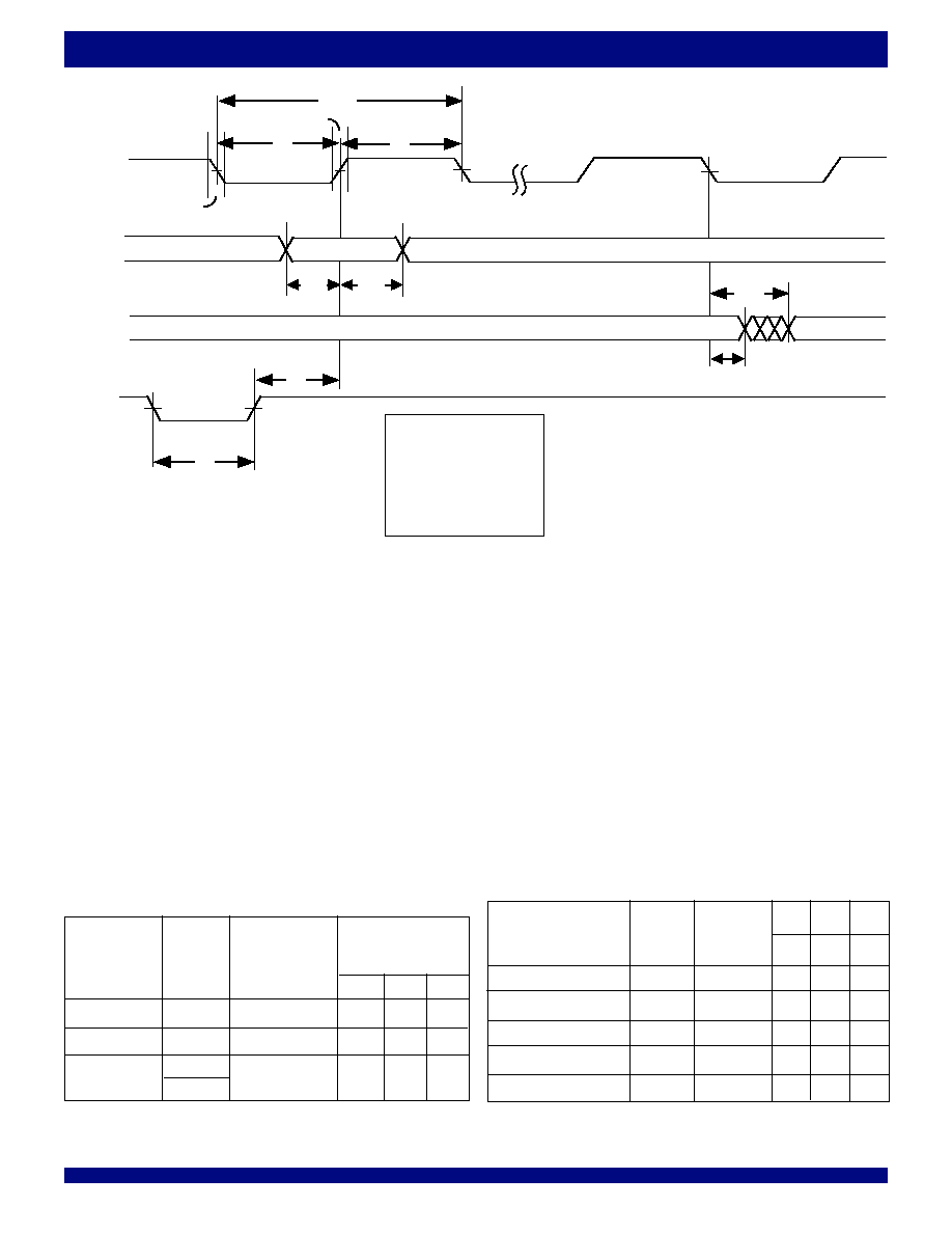
28
COMMERCIAL AND INDUSTRIAL
TEMPERATURE RANGES
IDT72T51248/72T51258/72T51268 2.5V MULTI-QUEUE DDR FLOW-CONTROL DEVICES
8,192 x 40 x 4, 16,384 x 40 x 4 and 32,768 x 40 x 4
t
4
t
3
TDO
TDO
TDI/
TMS
TCK
TRST
t
DOH
Notes to diagram:
t1 =
t
TCKLOW
t2 =
t
TCKHIGH
t3 =
t
TCKFALL
t4 = t
TCKRISE
t5 =
tRST
(reset pulse width)
t6 = tRSR (reset recovery)
6159 drw14
t
5
t
6
t
1
t
2
t
TCK
t
DH
t
DS
t
DO
Figure 7. Standard JTAG Timing
Parameter
Symbol
Test
Conditions
Min.
Max. Units
JTAG Clock Input Period t
TCK
-
100
-
ns
JTAG Clock HIGH
t
TCKHIGH
-
40
-
ns
JTAG Clock Low
t
TCKLOW
-
40
-
ns
JTAG Reset
t
RST
-
50
-
ns
JTAG Reset Recovery
t
RSR
-
50
-
ns
JTAG
AC ELECTRICAL CHARACTERISTICS
(
V
CC
= 2.5V
Ī
5%; Tambient (Industrial) = 0įC to +85įC)
NOTE:
1. 50pf loading on external output signals.
SYSTEM INTERFACE PARAMETERS
IDT72T51248
IDT72T51258
IDT72T51268
Parameter
Symbol
Test Conditions
Min.
Max.
Units
Data Output
t
DO
(1)
-
20
ns
Data Output Hold
t
DOH
(1)
0
-
ns
Data Input
t
DS
t
rise=3ns
10
-
ns
t
DH
t
fall=3ns
10
-
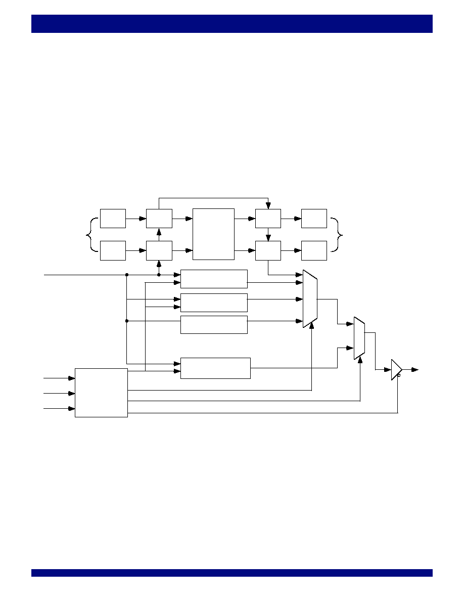
29
COMMERCIAL AND INDUSTRIAL
TEMPERATURE RANGES
IDT72T51248/72T51258/72T51268 2.5V MULTI-QUEUE DDR FLOW-CONTROL DEVICES
8,192 x 40 x 4, 16,384 x 40 x 4 and 32,768 x 40 x 4
JTAG TIMING SPECIFICATIONS
(IEEE 1149.1 COMPLIANT)
The JTAG test port in this device is fully compliant with the IEEE Standard
Test Access Port (IEEE 1149.1) specifications. Five additional pins (TDI, TDO,
TMS, TCK and
TRST) are provided to support the JTAG boundary scan
interface. Note that IDT provides appropriate Boundary Scan Description
Language program files for these devices.
The Standard JTAG interface consists of seven basic elements:
∑
Test Access Port (TAP)
∑
TAP controller
∑
Instruction Register (IR)
∑
Data Register Port (DR)
∑
Bypass Register (BYR)
∑
ID Code Register
∑
Flag Programming
The following sections provide a brief description of each element. For a
complete description refer to the IEEE Standard Test Access Port Specification
(IEEE Std. 1149.1-1990).
The Figure below shows the standard Boundary-Scan Architecture
Figure 8. JTAG Architecture
TEST ACCESS PORT (TAP)
The TAP interface is a general-purpose port that provides access to the
internal JTAG state machine. It consists of four input ports (TCLK, TMS, TDI,
TRST) and one output port (TDO).
THE TAP CONTROLLER
The TAP controller is a synchronous finite state machine that responds to
TMS and TCLK signals to generate clock and control signals to the Instruction
and Data Registers for capture and updating of data passed through the TDI
serial input.
In Pad
In Pad
Incell
Incell
Core
Logic
Outcell
Outcell
Out Pad
Out Pad
All outputs
All inputs
Eg: Dins, Clks
(BSDL file
describes the
chain order)
ID
Bypass
Instruction
Register
TAP
TMS
TDI
TCK
TRST
Instruction
Select
Enable
TDO
6159 drw15
Flag Offset Chain

30
COMMERCIAL AND INDUSTRIAL
TEMPERATURE RANGES
IDT72T51248/72T51258/72T51268 2.5V MULTI-QUEUE DDR FLOW-CONTROL DEVICES
8,192 x 40 x 4, 16,384 x 40 x 4 and 32,768 x 40 x 4
Refer to the IEEE Standard Test Access Port Specification (IEEE Std.
1149.1) for the full state diagram
All state transitions within the TAP controller occur at the rising edge of the
TCLK pulse. The TMS signal level (0 or 1) determines the state progression
that occurs on each TCLK rising edge. The TAP controller takes precedence
over the Queue operation and must be reset after power up of the device. See
TRST description for more details on TAP controller reset.
Test-Logic-Reset All test logic is disabled in this controller state enabling the
normal operation of the IC. The TAP controller state machine is designed in such
a way that, no matter what the initial state of the controller is, the Test-Logic-Reset
state can be entered by holding TMS at high and pulsing TCK five times. This
is the reason why the Test Reset (
TRST) pin is optional.
Run-Test-Idle In this controller state, the test logic in the IC is active only if
certain instructions are present. For example, if an instruction activates the self
test, then it will be executed when the controller enters this state. The test logic
in the IC is idle otherwise.
Select-DR-Scan This is a controller state where the decision to enter the
Data Path or the Select-IR-Scan state is made.
Select-IR-Scan This is a controller state where the decision to enter the
Instruction Path is made. The Controller can return to the Test-Logic-Reset state
other wise.
Figure 9. TAP Controller State Diagram
Capture-IR In this controller state, the shift register bank in the Instruction
Register parallel loads a pattern of fixed values on the rising edge of TCK. The
last two significant bits are always required to be "01".
Shift-IR In this controller state, the instruction register gets connected
between TDI and TDO, and the captured pattern gets shifted on each rising edge
of TCK. The instruction available on the TDI pin is also shifted in to the instruction
register. TDO changes on the falling edge of TCK.
Exit1-IR This is a controller state where a decision to enter either the Pause-
IR state or Update-IR state is made.
Pause-IR This state is provided in order to allow the shifting of instruction
register to be temporarily halted.
Exit2-DR This is a controller state where a decision to enter either the Shift-
IR state or Update-IR state is made.
Update-IR In this controller state, the instruction in the instruction register scan
chain is latched in to the register of the Instruction Register on every falling edge
of TCK. This instruction also becomes the current instruction once it is latched.
Capture-DR In this controller state, the data is parallel loaded in to the data
registers selected by the current instruction on the rising edge of TCK.
Shift-DR, Exit1-DR, Pause-DR, Exit2-DR and Update-DR These
controller states are similar to the Shift-IR, Exit1-IR, Pause-IR, Exit2-IR and
Update-IR states in the Instruction path.
Test-Logic
Reset
Run-Test/
Idle
1
0
0
Select-
DR-Scan
Select-
IR-Scan
1
1
1
Capture-IR
0
Capture-DR
0
0
Exit1-DR
1
Pause-DR
0
Exit2-DR
1
Update-DR
1
Exit1-IR
1
Exit2-IR
1
Update-IR
1
1
0
1
1
1
6159 drw16
0
Shift-DR
0
0
0
Shift-IR
0
0
Pause-IR
0
1
Input is
TMS
0
0
1
NOTES:
1. Five consecutive TCK cycles with TMS = 1 will reset the TAP.
2. TAP controller automatically resets upon power-up.
3. TAP controller must be reset before normal Queue operations can begin.
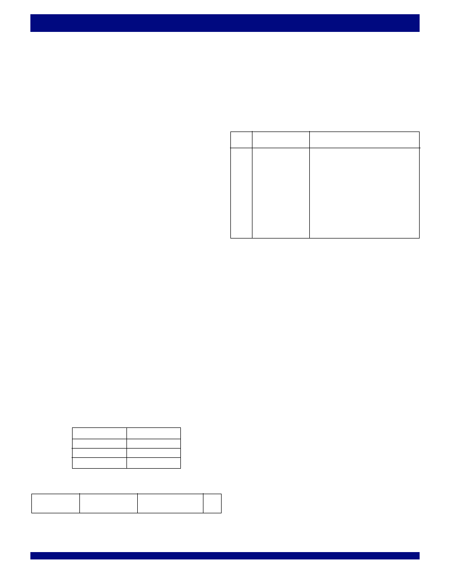
31
COMMERCIAL AND INDUSTRIAL
TEMPERATURE RANGES
IDT72T51248/72T51258/72T51268 2.5V MULTI-QUEUE DDR FLOW-CONTROL DEVICES
8,192 x 40 x 4, 16,384 x 40 x 4 and 32,768 x 40 x 4
THE INSTRUCTION REGISTER
The instruction register (IR) is eight bits long and tells the device what
instruction is to be executed. Information contained in the instruction includes the
mode of operation (either normal mode, in which the device performs its normal
logic function, or test mode, in which the normal logic function is inhibited or
altered), the test operation to be performed, which of the four data registers is
to be selected for inclusion in the scan path during data-register scans, and the
source of data to be captured into the selected data register during Capture-DR.
TEST DATA REGISTER
The Test Data register contains three test data registers: the Bypass, the
Boundary Scan register and Device ID register.
These registers are connected in parallel between a common serial input
and a common serial data output.
The following sections provide a brief description of each element. For a
complete description, refer to the IEEE Standard Test Access Port Specification
(IEEE Std. 1149.1-1990).
TEST BYPASS REGISTER
The register is used to allow test data to flow through the device from TDI
to TDO. It contains a single stage shift register for a minimum length in the serial
path. When the bypass register is selected by an instruction, the shift register
stage is set to a logic zero on the rising edge of TCLK when the TAP controller
is in the Capture-DR state.
The operation of the bypass register should not have any effect on the
operation of the device in response to the BYPASS instruction.
THE BOUNDARY-SCAN REGISTER
The boundary-scan register (BSR) is 48 bits long. It contains one
boundary-scan cell (BSC) for each normal-function input pin and one BSC for
each normal-function I/O pin (one single cell for both input data and output data).
The BSR is used 1) to store test data that is to be applied externally to the device
output pins, and/or 2) to capture data that appears internally at the outputs of
the normal on-chip logic and/or externally at the device input pins.
THE DEVICE IDENTIFICATION REGISTER
The Device Identification Register is a Read Only 32-bit register used to
specify the manufacturer, part number and version of the device to be
determined through the TAP in response to the IDCODE instruction.
IDT JEDEC ID number is 0xB3. This translates to 0x33 when the parity is
dropped in the 11-bit Manufacturer ID field.
For the IDT72T51248/72T51258/72T51268, the Part Number field con-
tains the following values:
IDT72T51248/258/268 JTAG Device Identification Register
31(MSB)
28 27
12 11
1 0(LSB)
Version (4 bits)
Part Number (16-bit) Manufacturer ID (11-bit)
0000
0033 (hex)
1
JTAG INSTRUCTION REGISTER
The Instruction register allows an instruction to be serially input into the
device when the TAP controller is in the Shift-IR state. The instruction is decoded
to perform the following:
∑
Select test data registers that may operate while the instruction is
current. The other test data registers should not interfere with chip
operation and the selected data register.
∑
Define the serial test data register path that is used to shift data between
TDI and TDO during data register scanning.
The Instruction Register is a 4 bit field (i.e. IR3, IR2, IR1, IR0) to decode
16 different possible instructions. Instructions are decoded as follows.
Hex
Instruction
Function
Value
0000
EXTEST
Test external pins
0001
SAMPLE/PRELOAD Select boundary scan register
0002
IDCODE
Selects chip identification register
0003
CLAMP
Fix the output chains to scan chain values
0004
HIGH-IMPEDANCE Puts all outputs in high-impedance state
0007
OFFSET READ
Read
PAE/PAF offset register values
0008
OFFSET WRITE
Write
PAE/PAF offset register values
000F
BYPASS
Select bypass register
Private
Several combinations are private (for IDT
internal use). Do not use codes other than
those identified above.
JTAG Instruction Register Decoding
The following sections provide a brief description of each instruction. For
a complete description refer to the IEEE Standard Test Access Port Specification
(IEEE Std. 1149.1-1990).
EXTEST
The required EXTEST instruction places the device into an external
boundary-test mode and selects the boundary-scan register to be connected
between TDI and TDO. During this instruction, the boundary-scan register is
accessed to drive test data off-chip via the boundary outputs and receive test
data off-chip via the boundary inputs. As such, the EXTEST instruction is the
workhorse of IEEE. Std 1149.1, providing for probe-less testing of solder-joint
opens/shorts and of logic cluster function.
SAMPLE/PRELOAD
The required SAMPLE/PRELOAD instruction allows the device to remain in
a normal functional mode and selects the boundary-scan register to be
connected between TDI and TDO. During this instruction, the boundary-scan
register can be accessed via a data scan operation, to take a sample of the
functional data entering and leaving the device. This instruction is also used to
preload test data into the boundary-scan register before loading an EXTEST
instruction.
IDCODE
The optional IDCODE instruction allows the device to remain in its functional
mode and selects the optional device identification register to be connected
between TDI and TDO. The device identification register is a 32-bit shift register
containing information regarding the device manufacturer, device type, and
version code. Accessing the device identification register does not interfere with
the operation of the device. Also, access to the device identification register
should be immediately available, via a TAP data-scan operation, after power-
up of the device or after the TAP has been reset using the optional
TRST pin
or by otherwise moving to the Test-Logic-Reset state.
Device
Part# Field
IDT72T51248
04C1 (hex)
IDT72T51258
04C2 (hex)
IDT72T51268
04C3 (hex)

32
COMMERCIAL AND INDUSTRIAL
TEMPERATURE RANGES
IDT72T51248/72T51258/72T51268 2.5V MULTI-QUEUE DDR FLOW-CONTROL DEVICES
8,192 x 40 x 4, 16,384 x 40 x 4 and 32,768 x 40 x 4
CLAMP
The optional CLAMP instruction sets the outputs of an device to logic levels
determined by the contents of the boundary-scan register and selects the one-
bit bypass register to be connected between TDI and TDO. Before loading this
instruction, the contents of the boundary-scan register can be preset with the
SAMPLE/PRELOAD instruction. During this instruction, data can be shifted
through the bypass register from TDI to TDO without affecting the condition of
the outputs.
HIGH-IMPEDANCE
The optional High-Impedance instruction sets all outputs (including two-state
as well as three-state types) of an device to a disabled (high-impedance) state
and selects the one-bit bypass register to be connected between TDI and TDO.
During this instruction, data can be shifted through the bypass register from TDI
to TDO without affecting the condition of the device outputs.
OFFSET READ
This instruction is an alternative to serial reading the offset registers for the
PAE/PAF flags. When reading the offset registers through this instruction, the
dedicated serial programming signals must be disabled.
OFFSET WRITE
This instruction is an alternative to serial programming the offset registers for
the
PAE/PAF flags. When writing the offset registers through this instruction, the
dedicated serial programming signals must be disabled.
BYPASS
The required BYPASS instruction allows the device to remain in a normal
functional mode and selects the one-bit bypass register to be connected
between TDI and TDO. The BYPASS instruction allows serial data to be
transferred through the IC from TDI to TDO without affecting the operation of
the device.

33
COMMERCIAL AND INDUSTRIAL
TEMPERATURE RANGES
IDT72T51248/72T51258/72T51268 2.5V MULTI-QUEUE DDR FLOW-CONTROL DEVICES
8,192 x 40 x 4, 16,384 x 40 x 4 and 32,768 x 40 x 4
EF/OR
(8)
0/1/2/3
t
RSF
If FWFT = HIGH,
OR = HIGH
If FWFT = LOW,
EF = LOW
t
RSF
PAF
(8)
0/1/2/3
t
RSF
t
RSF
Q[39:0]
t
RSF
OE = HIGH
OE = LOW
6159 drw17
OW[1:0]
(4)
,
IW[1:0]
(4)
FSEL[1:0]
(4)
PFM
(4)
HIGH = Synchronous
PAE/PAF Timing
LOW = Asynchronous
PAE/PAF Timing
HIGH = FWFT Mode
LOW = IDT Standard Mode
RDDR
(4)
,
WDDR
(4)
FWFT/SI
(4)
IOSEL
(4)
HIGH = Read/Write Double Data Rate
LOW = Read/Write Single Data Rate
HIGH = HSTL I/Os
LOW = LVTTL I/Os
t
RSS
t
RSS
t
RSS
t
RSS
t
RSS
t
RSS
If FWFT = LOW,
FF = HIGH
If FWFT = HIGH,
IR = LOW
FF/IR
(8)
0/1/2/3
PAE
(8)
0/1/2/3
IS[1:0]
(4)
,
OS[1:0]
(4)
t
RSS
t
RS
MRS
WEN
REN
(7)
t
RSS
SWEN,
SREN
t
RSS
t
RSR
t
RSR
Figure 10. Master Reset Timing
NOTES:
1.
OE can toggle during master reset. During master reset, the high-impedance control of the Qn data outputs is provided by OE only.
2.
PRS should be HIGH during a MRS.
3. RCLK, WCLK and SCLK can be free running or idle.
4. The state of these pins are latched when the master reset pulse is LOW.
5. JTAG clock should not toggle during master reset.
6.
RCS and WCS can be HIGH or LOW until the first rising edge of RCLK after master reset is complete.
7.
EREN wave form is identical to REN, ERCLK wave form is identical to RCLK.
8. Composite flag wave form is identical to
EF, FF, PAE, PAF wave form above.
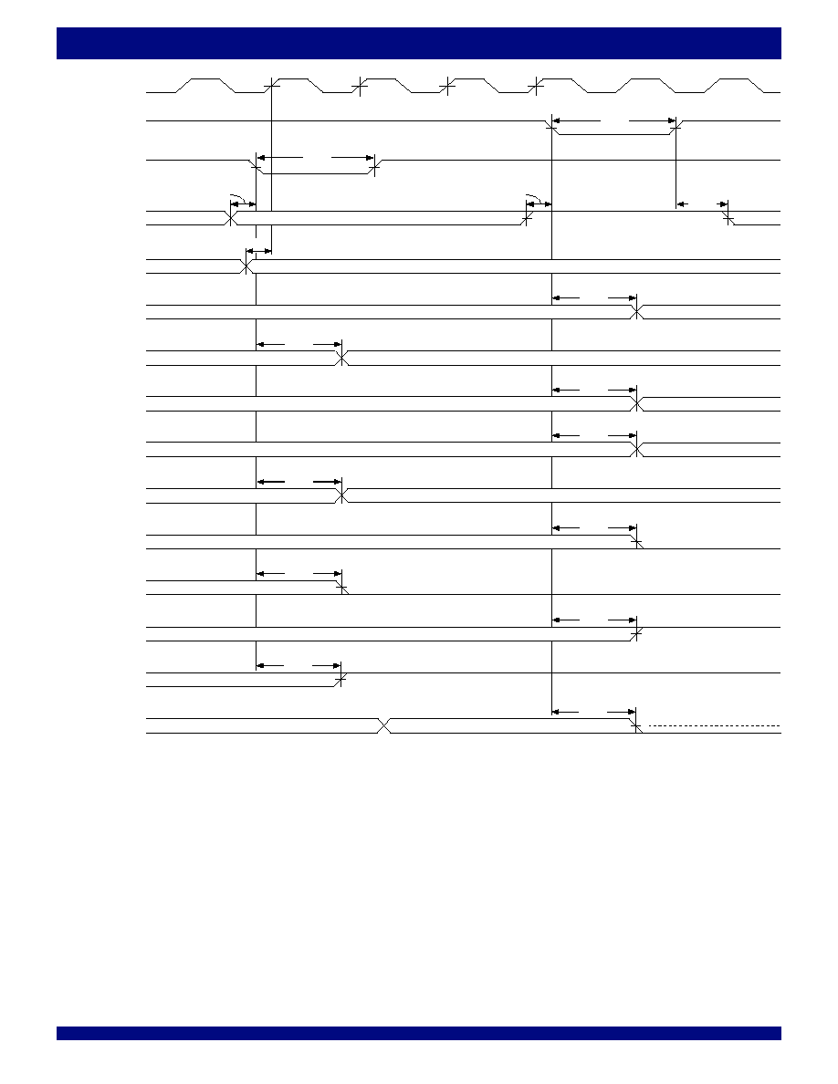
34
COMMERCIAL AND INDUSTRIAL
TEMPERATURE RANGES
IDT72T51248/72T51258/72T51268 2.5V MULTI-QUEUE DDR FLOW-CONTROL DEVICES
8,192 x 40 x 4, 16,384 x 40 x 4 and 32,768 x 40 x 4
WEN,
REN
t
RSS
PRS2/3
(1)
t
RSS
t
RSR
RCLK
1
2
3
PRS0/1
(1,3)
t
RS
4
6159 drw18
FF/IR0/1
t
RSF
Current State
Current State
FF/IR2/3
t
RSF
If FWFT = HIGH,
FF = HIGH
If FWFT = LOW,
IR = LOW
If FWFT = HIGH,
CFF = HIGH
If FWFT = LOW,
CIR = LOW
PAE0/1
t
RSF
Current State
PAE2/3
t
RSF
PAF0/1
t
RSF
Current State
PAF2/3
t
RSF
Q[39-0]
(2,4)
t
RSF
OE = HIGH
OE = LOW
Current State
Current State
OS[1:0],
IS[1:0]
t
ENS
00 = Queue 0
01 = Queue 1
EF/OR0/1
t
RSF
Current State
Current State
EF/OR2/3
t
RSF
If FWFT = HIGH,
OR = HIGH
If FWFT = LOW,
EF = LOW
If FWFT = HIGH,
OR = HIGH
If FWFT = LOW,
EF = LOW
CEF/COR
t
RSF
Current State
If FWFT = HIGH,
COR = HIGH
If FWFT = LOW,
CEF = LOW
Output Data Queue 0
Output Data Queue 1
t
RS
Figure 11. Partial Reset Timing
NOTES:
1. During the input and/or output selection of two Queues, partial reset of the two Queues involved are prohibited.
2. During partial reset the high-impedance control of the output is provided by
OE only.
3.
PRS0/1 must go LOW after the fourth rising edge of RCLK/WCLK from where IS[1:0] and/or OS[1:0] transitioned.
4. This is the output data from Queue0 and Queue1.
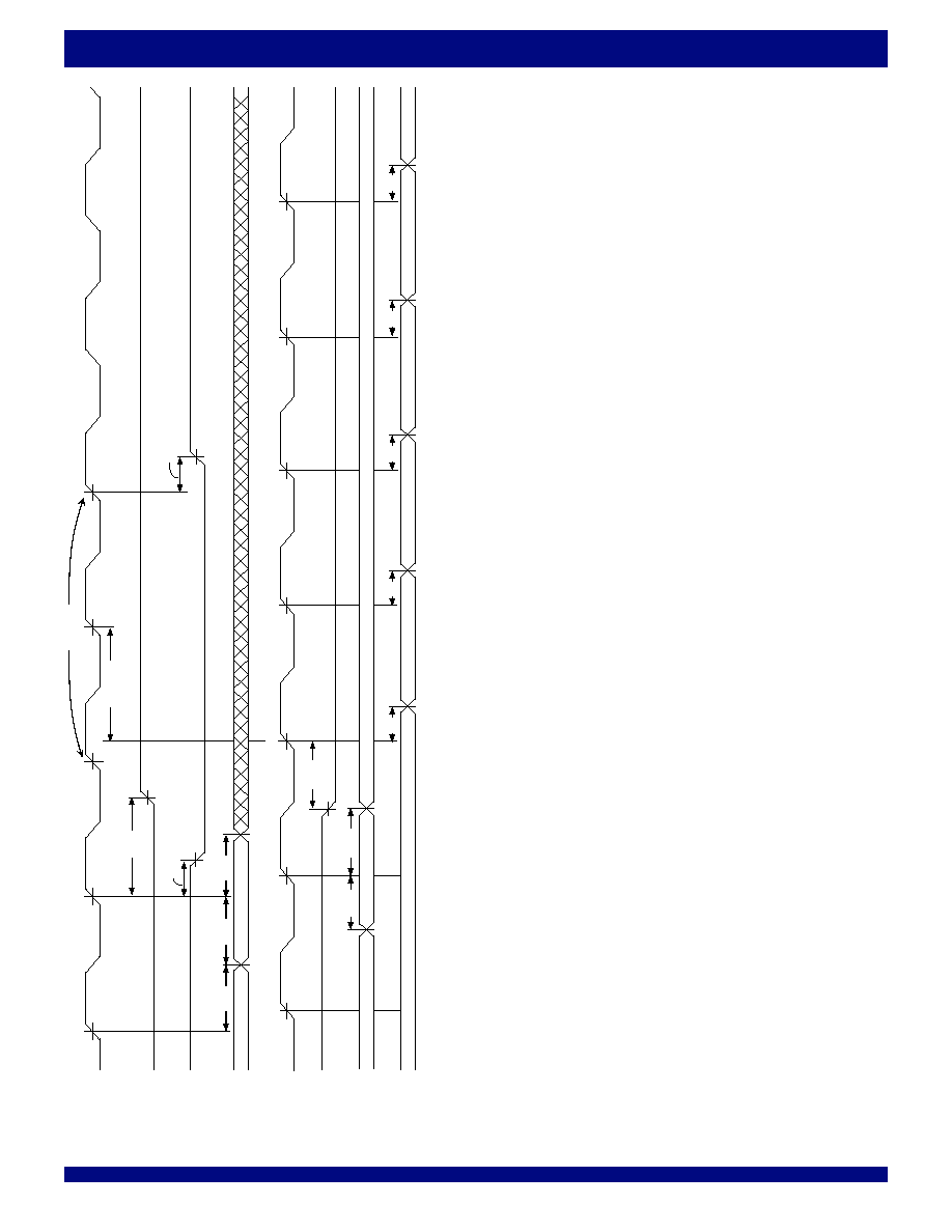
35
COMMERCIAL AND INDUSTRIAL
TEMPERATURE RANGES
IDT72T51248/72T51258/72T51268 2.5V MULTI-QUEUE DDR FLOW-CONTROL DEVICES
8,192 x 40 x 4, 16,384 x 40 x 4 and 32,768 x 40 x 4
Figure 12. Write Cycle and Full Flag Timing (IDT Standard mode, SDR to SDR, x40 In to x40 Out)
WEN
D[39:0]
W
D-1
WCLK
No Write
FF
0
t
WFF
t
DH
t
DS
W
D
OS[1:0]
00=Queue 0
t
A
6157 drw19
RCLK
REN
01=Queue 1
Q[39:0]
(4)
Previous Word Queue 0
t
A
t
A
Word 0 Queue 2
t
A
Word 1 Queue 2
t
A
t
ENH
t
WFF
t
ENS
t
DH
t
SKEW1
(3)
t
ENS
t
ENH
10=Queue 2
Word 2 Queue 2
Q0
Q0
Q0
Q1
Q2
Q3
Q4
Previous Word + 1 Queue 0
W
ord 0 Queue 1
NOTES:
1.
WCS
= LOW,
OE
= LOW, WDDR = LOW, RDDR = LOW, and IS[1:0] = 00.
2
.
WCLK must be free running for
FF
0 to update.
3.
t
SKEW1
, is the minimum time between a rising RCLK edge and a rising WCLK edge to guarantee that
FF
0 will go HIGH (after one WCLK cycle plus t
WFF
). If the time between the rising edge of RCLK and the rising edge of WCLK
is less than t
SKEW1
, then the
FF
0 deassertion may be delayed one extra WCLK cycle. (See Table 6 - T
SKEW
measurement).
4
.
Two stage pipeline causes a two-cycle latency on wrtie operations.
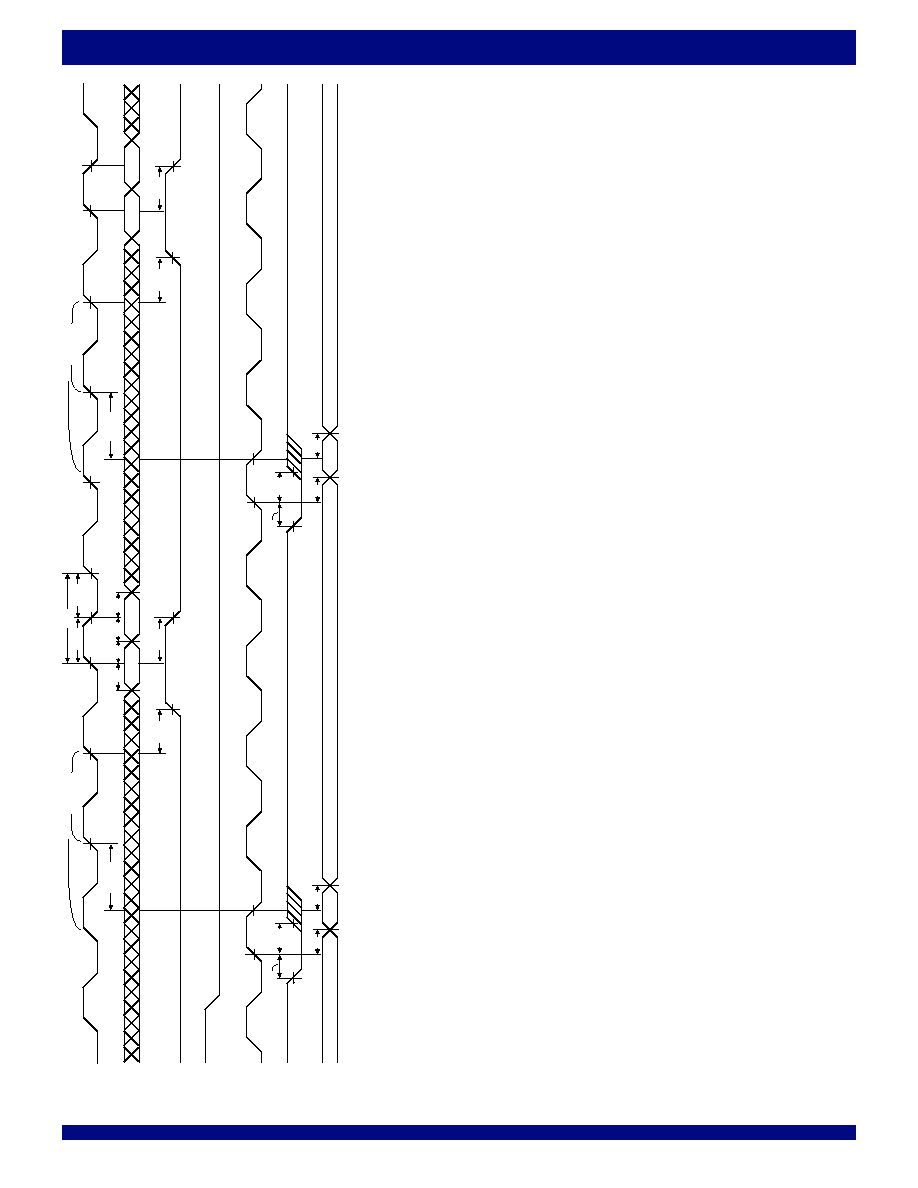
36
COMMERCIAL AND INDUSTRIAL
TEMPERATURE RANGES
IDT72T51248/72T51258/72T51268 2.5V MULTI-QUEUE DDR FLOW-CONTROL DEVICES
8,192 x 40 x 4, 16,384 x 40 x 4 and 32,768 x 40 x 4
Figure 13. Write Cycle and Full Flag Timing in DDR mode ( IDT Standard mode, DDR to DDR, x40 In to x40 Out)
NOTES:
1.
t
SKEW2
is the minimum time between a falling RCLK edge and a rising WCLK edge to guarantee that
FF
0 will go HIGH (after one WCLK cycle plus t
WFF
). If the time between the falling edge of the RCLK and the rising edge of WCLK
is less than t
SKEW2
, then
FF
0 deassertion may be delayed one extra WCLK cycle. (See Table 6 - T
SKEW
measurement).
2.
OE
0 = LOW,
WCS
= LOW,
RCS
= LOW, WDDR = HIGH, RDDR = HIGH, IS[1:0] = 00, and OS[1:0] = 00.
3
.
WCLK must be free running for
FF
0 to update.
Word 1
Q[39:0]
6159 drw20
t
A
12
NO WRITE
D[39:0]
RCLK
WCLK
WEN
FF
0
t
CLKL
t
CLKH
t
CLK
t
SKEW2
(1)
12
t
SKEW2
(1)
REN
NO WRITE
W
D
t
DS
t
DS
t
DH
W
D
+1
t
DH
W
D
+2
W
D
+3
t
WFF
t
WFF
t
WFF
t
WFF
t
ENH
t
ENS
t
ENH
t
ENS
t
A
Data in Output Register
Word 2
Word 3
t
A
t
A
Word 4

37
COMMERCIAL AND INDUSTRIAL
TEMPERATURE RANGES
IDT72T51248/72T51258/72T51268 2.5V MULTI-QUEUE DDR FLOW-CONTROL DEVICES
8,192 x 40 x 4, 16,384 x 40 x 4 and 32,768 x 40 x 4
Figure 14. Write Cycle and Full Flag Timing with bus-matching and rate matching (IDT Standard mode, DDR to SDR, x10 In to x20
Out)
WCLK
FF
0
WEN
RCS
t
ENS
t
SKEW1
(1)
Q[39:0]
RCLK
t
ENH
t
ENS
1
2
t
WFF
D[39:0]
REN
t
RCSLZ
t
A
t
DS
t
DS
t
DH
t
DH
t
WFF
t
SKEW1
(1)
t
ENS
t
ENH
t
A
1
2
t
WFF
t
DS
t
DS
t
DH
t
DH
t
CLK
t
CLKH
t
CLKL
NO WRITE
NO WRITE
t
WFF
W
Y
W
Y
+ 1
Wx
Wx+1
Wx+2
Wx+3
6159 drw21
NOTES:
1.
t
SKEW1
is the minimum time between a rising RCLK edge and a rising WCLK edge to guarantee that
FF
0 will go HIGH (after one WCLK cycle plus t
WFF
). If the time between the rising edge of the RCLK and the rising edge of the
WCLK is less than t
SKEW1
, then the
FF
0 deassertion may be delayed one extra WCLK cycle. (See Table 6 - T
SKEW
measurement).
2.
OE
0 = LOW,
WCS
= LOW, WDDR = HIGH, RDDR = LOW, IS[1:0] = 00, and OS[1:0] = 00.
3
.
WCLK must be free running for
FF
0 to update.
4.
W
X
is a 10 bit word. D[39:10] are not used and should be corrected to GND.
5.
W
Y
is a 20 bit word. Q[39:20] are not used and should be left open.

38
COMMERCIAL AND INDUSTRIAL
TEMPERATURE RANGES
IDT72T51248/72T51258/72T51268 2.5V MULTI-QUEUE DDR FLOW-CONTROL DEVICES
8,192 x 40 x 4, 16,384 x 40 x 4 and 32,768 x 40 x 4
Figure 15. Write Cycle and Full Flag Timing with rate matching (IDT Standard mode, SDR to DDR, x40 In to x40 Out)
WCLK
FF
0
WEN
RCS
t
ENS
Q[39:0]
RCLK
t
ENH
t
ENS
1
2
t
WFF
D[39:0]
REN
t
RCSLZ
t
A
t
DS
t
DH
t
ENS
t
ENH
t
A
1
2
t
DS
t
DS
t
DH
t
DH
t
CL
K
NO WRITE
NO WRITE
t
WFF
Word 1
Word 3
W
D
W
D
+2
W
D
+3
t
A
t
DS
t
DH
W
D
+1
t
CLKH
t
CLKH
t
WFF
t
A
t
SKEW2
(1)
t
WFF
t
ENS
t
RCSHZ
Word 0
Word 2
6159 drw22
t
SKEW2
(1)
NOTES:
1.
t
SKEW2
is the minimum time between a falling RCLK edge and a rising WCLK edge to guarantee that
FF
0 will go HIGH (after one WCLK cycle plus t
WFF
). If the time between the falling edge of the RCLK and the rising edge of WCLK
is less than t
SKEW2
, then
FF
0 deassertion may be delayed one extra WCLK cycle. (See Table 6 - T
SKEW
measurement).
2.
OE
0 = LOW,
WCS
= LOW,
RCS
= LOW, WDDR = LOW, RDDR = HIGH, IS[1:0] = 00, and OS[1:0] = 00.
3
.
WCLK must be free running for
FF0
to update.

39
COMMERCIAL AND INDUSTRIAL
TEMPERATURE RANGES
IDT72T51248/72T51258/72T51268 2.5V MULTI-QUEUE DDR FLOW-CONTROL DEVICES
8,192 x 40 x 4, 16,384 x 40 x 4 and 32,768 x 40 x 4
RCLK
t
SKEW1
Word 0
Q[39:0]
6159 drw23
t
A
Previous Data in Output Register
t
A
Word 1
t
A
Word 2
Word 3
REN
t
ENS
OR
0
t
REF
D[39:0]
WEN
WCLK
t
ENS
Word 1
t
DH
t
DS
Word 0
t
ENH
Word 2
Word 3
12
3
t
DH
t
A
t
REF
Figure 16. Write Timing in FWFT mode (FWFT mode, SDR to SDR, x40 In to x40 Out)
NOTES:
1.
t
SKEW
, is the minimum time between a rising RCLK edge and a rising WCLK edge to guarantee that
FF
0 will go HIGH (after one WCLK cycle plus t
WFF
). If the time between the rising edge of RCLK and the rising edge of WCLK
is less than t
SKEW1
, then the
FF
0 deassertion may be delayed one extra WCLK cycle. (See Table 6 - T
SKEW
measurement).
2.
WCS
= LOW,
OE
= LOW, WDDR = LOW, RDDR = LOW, IS[1:0] = 00, OS[1:0] = 0, and
RCS
= LOW.
3
.
WCLK must be free running for
FF
0 to update.

40
COMMERCIAL AND INDUSTRIAL
TEMPERATURE RANGES
IDT72T51248/72T51258/72T51268 2.5V MULTI-QUEUE DDR FLOW-CONTROL DEVICES
8,192 x 40 x 4, 16,384 x 40 x 4 and 32,768 x 40 x 4
Figure 17. Write Cycle and First Word Latency Timing in DDR mode (FWFT mode, DDR to DDR, x40 In to x40 Out)
NOTES:
1.
t
SKEW2
is the minimum time between a falling WCLK edge and a rising RCLK edge to guarantee that
OR
0 will go LOW after two RCLK cycle plus t
REF
. If the time between the falling edge of WCLK and the rising edge of RCLK
is less than t
SKEW2
, then
OR
0 assertion may be delayed one extra RCLK cycle. (See Table 6 - T
SKEW
measurement).
2.
OE
= LOW,
RCS
= LOW,
WCS
= LOW, WDDR = HIGH, RDDR = HIGH, IS[1:0] = 00, and OS[1:0] = 00.
3
.
First data word latency = t
SKEW2
+ RCLK full period + t
REF.
4
.
RCLK must be free running for
OR
0 to update.
WCLK
WEN
OR
0
t
SKEW2
(1)
Q[39:0]
RCLK
D[39:0]
REN
Previous Data In Output Register
6159 drw24
t
DS
t
DH
Word 1
Word 2
t
ENH
12
3
t
DS
t
DH
t
DS
t
DH
Word 3
Word 4
t
ENH
t
DS
t
DH
t
ENS
t
ENS
t
REF
t
REF
t
ENH
t
ENS
t
A
t
A
Word 1
Word 2
t
A
t
A
Word 3
Word 4
t
SKEW2
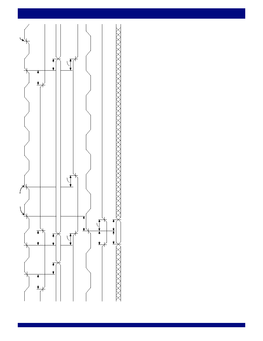
41
COMMERCIAL AND INDUSTRIAL
TEMPERATURE RANGES
IDT72T51248/72T51258/72T51268 2.5V MULTI-QUEUE DDR FLOW-CONTROL DEVICES
8,192 x 40 x 4, 16,384 x 40 x 4 and 32,768 x 40 x 4
RCLK
REN
12
EF
0
t
REF
t
REF
t
REF
WEN
D[39:0]
Q[39:0]
t
A
No Read
No Read
t
A
W
D+
1
WCLK
t
ENH
t
DH
W
D+
1
6159 drw25
t
A
t
DS
t
ENS
t
ENS
t
SKEW
t
ENH
t
ENS
W
D
W
D-1
W
D-2
Figure 18. Read Cycle, Empty Flag and First Word Latency (IDT Standard mode, SDR to SDR, x40 In to x40 Out)
NOTES:
1.
OE
= LOW,
RCS
= LOW,
WCS
= LOW, WDDR = LOW, RDDR = LOW, IS[1:0] = 00, and OS[1:0] = 00.
2
.
First data word latency = t
SKEW1
+ RCLK full period + t
REF.
3
.
RCLK must be free running for
EF
0 to update.

42
COMMERCIAL AND INDUSTRIAL
TEMPERATURE RANGES
IDT72T51248/72T51258/72T51268 2.5V MULTI-QUEUE DDR FLOW-CONTROL DEVICES
8,192 x 40 x 4, 16,384 x 40 x 4 and 32,768 x 40 x 4
EF
0
Q[39:0]
WCLK
WEN
D[39:0]
Word 0
t
DS
REN
RCLK
t
SKEW2
12
t
REF
6159 drw26
t
A
Word 0
t
ENS
t
ENS
t
ENS
t
A
t
A
t
A
Word 1
W
ord 2
W
ord 3
t
REF
t
DH
Word 1
t
DS
t
DH
Word 2
t
DS
t
DH
Word 3
t
DS
t
DH
Figure 19. Read Cycle, Empty Flag and First Word Latency in DDR mode (IDT Standard mode, DDR to DDR, x40 In to x40 Out)
NOTES:
1.
t
SKEW2
is the minimum time between a falling RCLK edge and a rising WCLK edge to guarantee that
FF
0 will go HIGH (after one WCLK cycle plus t
WFF
). If the time between the
falling edge of the RCLK and the rising edge of WCLK is less than t
SKEW2
, then
FF
0 deassertion may be delayed one extra WCLK cycle. (See Table 6 - T
SKEW
measurement).
2.
OE
0 = LOW,
WCS
= LOW,
RCS
= LOW, WDDR = HIGH, RDDR = HIGH, IS[1:0] = 00, and OS[1:0] = 00.
3
.
First data word latency = t
SKEW2
+ RCLK full period + t
REF.
4
.
RCLK must be free running for
EF
0 to update.
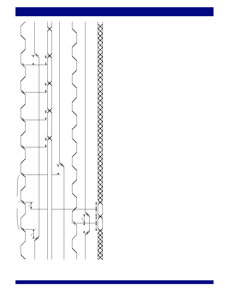
43
COMMERCIAL AND INDUSTRIAL
TEMPERATURE RANGES
IDT72T51248/72T51258/72T51268 2.5V MULTI-QUEUE DDR FLOW-CONTROL DEVICES
8,192 x 40 x 4, 16,384 x 40 x 4 and 32,768 x 40 x 4
Q[39:0]
(5)
WCLK
WEN
D[39:0]
6159 drw27
Word 0
t
DS
t
DH
t
ENH
t
ENS
EF
0
t
REF
REN
RCLK
t
SKEW2
12
Previous Data in Output Register
t
A
Word 0 (LSB)
t
A
t
ENS
t
REF
t
A
t
A
NO READ
Word 0 (MSB)
Word 1 (LSB)
W
ord 1 (MSB)
Word 1
t
DS
t
DH
Figure 20. Read Cycle, Empty Flag and First Word Latency with bus-matching and rate-matching (IDT Standard mode, DDR to SDR, x4
0 In to x20 Out)
NOTES:
1.
t
SKEW2
is the minimum time between a falling RCLK edge and a rising WCLK edge to guarantee that
FF
0 will go HIGH (after one WCLK cycle plus t
WFF
). If the time between the falling edge of the RCLK and the rising edge of WCLK
is less than t
SKEW2
, then
FF
0 deassertion may be delayed one extra WCLK cycle. (See Table 6 - T
SKEW
measurement).
2.
OE
= LOW,
WCS
= LOW,
RCS
= LOW, WDDR = HIGH, RDDR = HIGH, IW = 10, OW = 01, IS[1:0] = 00, and OS[1:0] = 00.
3
.
First data word latency = t
SKEW2
+ RCLK full period + t
REF.
4
.
RCLK must be free running for
EF
0 to update.
5
.
Word X LSB = D[19:0], Word X MSB = D[39:20], Q[39:20] will be high-impedanced.
6
.
Q[39:20] are not used and must be left open.

44
COMMERCIAL AND INDUSTRIAL
TEMPERATURE RANGES
IDT72T51248/72T51258/72T51268 2.5V MULTI-QUEUE DDR FLOW-CONTROL DEVICES
8,192 x 40 x 4, 16,384 x 40 x 4 and 32,768 x 40 x 4
Figure 21. Read Cycle and Empty Flag Timing with bus-matching and rate-matching (IDT Standard mode, SDR to DDR, x10 In to x20
Out)
NOTES:
1.
t
SKEW1
is the minimum time between a rising WCLK edge and a rising RCLK edge to guarantee that
EF
0 will go HIGH (after one RCLK cycle plus t
REF
). If the time between the rising edge of WCLK and the rising edge of
RCLK is less than t
SKEW1
, then
EF
0 deassertion may be delayed one extra RCLK cycle. (See Table 6 - T
SKEW
measurement).
2.
OE
0 = LOW,
RCS
= LOW,
WCS
= LOW, WDDR = LOW, RDDR = HIGH, IW = 00, and OW = 01.
3
.
First data word latency = t
SKEW1
+ RCLK full period + t
REF
.
4
.
RCLK must be free running for
EF
0 to update.
5
.
Word WX LSB = D[9:0], Word WX MSB = D[19:10].
6
.
D[39:10] are not used and should be tied to GND. Q[39:20] are not used and must be left open.
Q[39:0]
t
SKEW1
(1)
WCLK
RCLK
REN
12
WEN
t
REF
EF
0
D[39:0]
6159 drw28
t
REF
t
REF
Last Word
(
L
SB)
Last 20-bit Word (MSB)
t
ENS
t
ENH
W
0
(LSB)
W
0
(MSB)
W
1
(LSB)
t
ENH
t
ENS
W
0
(
MSB,LSB)
t
A
t
A
t
A
t
A
t
DS
t
DH
t
DS
t
DH
t
DS
t
DH
t
DH
t
DS
t
CLK
t
CLKH
t
CLKL
Previous Data
t
ENH
NO Read
W
1
(MSB)
W
1
(
MSB,LSB)

45
COMMERCIAL AND INDUSTRIAL
TEMPERATURE RANGES
IDT72T51248/72T51258/72T51268 2.5V MULTI-QUEUE DDR FLOW-CONTROL DEVICES
8,192 x 40 x 4, 16,384 x 40 x 4 and 32,768 x 40 x 4
6159 drw29
t
A
Word 0
t
A
t
ENS
t
A
RCLK
Q[39:0]
REN
IR0
t
WFF
t
WFF
t
SKEW1
1
2
D[39:0]
WEN
WCLK
Word D+1
t
ENH
t
ENS
t
DH
t
DS
Word 1
Word 2
Word 3
Figure 22. Read Timing at Full Boundary (FWFT mode, SDR to SDR, x40 In to x40 Out)
NOTES:
1. t
SKEW1
, is the minimum time between a rising RCLK edge and a rising WCLK edge to guarantee that
IR0 will go HIGH (after one WCLK cycle plus t
WFF
). If the time between the
rising edge of RCLK and the rising edge of WCLK is less than t
SKEW1
, then the
IR0 deassertion may be delayed one extra WCLK cycle. (See Table 6 - t
SKEW
measurement).
2. WCLK must be free running for
IR0 to update.
3.
OE = LOW, RCS = LOW, WCS = LOW, WDDR = LOW, RDDR = LOW, IW = 10, and OW = 10.

46
COMMERCIAL AND INDUSTRIAL
TEMPERATURE RANGES
IDT72T51248/72T51258/72T51268 2.5V MULTI-QUEUE DDR FLOW-CONTROL DEVICES
8,192 x 40 x 4, 16,384 x 40 x 4 and 32,768 x 40 x 4
REN
EF1
RCLK
t
A
6159 drw30
1
2
3
Q[39:0]
Word
D-1
Queue 1
OS[1:0]
01 = Queue 1
Word D Queue 1
t
ENS
t
A
Word A Queue 3
t
REF
CEF
t
REF
t
REF
No Read
t
DS
11 = Queue 3
Queue 1 Status
Queue 3 Status
Figure 23. Composite Empty Flag (IDT Standard mode, SDR to SDR, x40 In to x40 Out)
NOTES:
1.
RCS = LOW, and OE = LOW.
2.
EF3 is HIGH.
3. Word D-1 is the second to last word in Queue 1. Word D is the last word in Queue 1.
4. Word A is the next available word in Queue 3.
5. The composite empty flag will update to the newly selected Queue after one RCLK cycle once a new Queue has been selected using OS[1:0].
REN
OR1
RCLK
t
A
6159 drw31
1
2
3
Q[39:0]
Word
D-1
Queue 1
OS[1:0]
01 = Queue 1
11 = Queue 3
Word D Queue 1
t
ENS
t
ENS
t
A
Word A Queue 3
t
REF
COR
t
REF
t
REF
Queue 1 Status
Queue 3 Status
Figure 24. Composite Output Ready Flag (FWFT mode, SDR to SDR, x40 In to x40 Out)
NOTES:
1.
RCS = LOW, and OE = LOW.
2.
OR3 is LOW.
3. Word D-1 is the second to last word in Queue 1. Word D is the last word in Queue 1.
4. Word A is the next available word in Queue 3.
5. The composite output ready flag will update to the newly selected Queue after two RCLK cycles once a new Queue has been selected using OS[1:0].
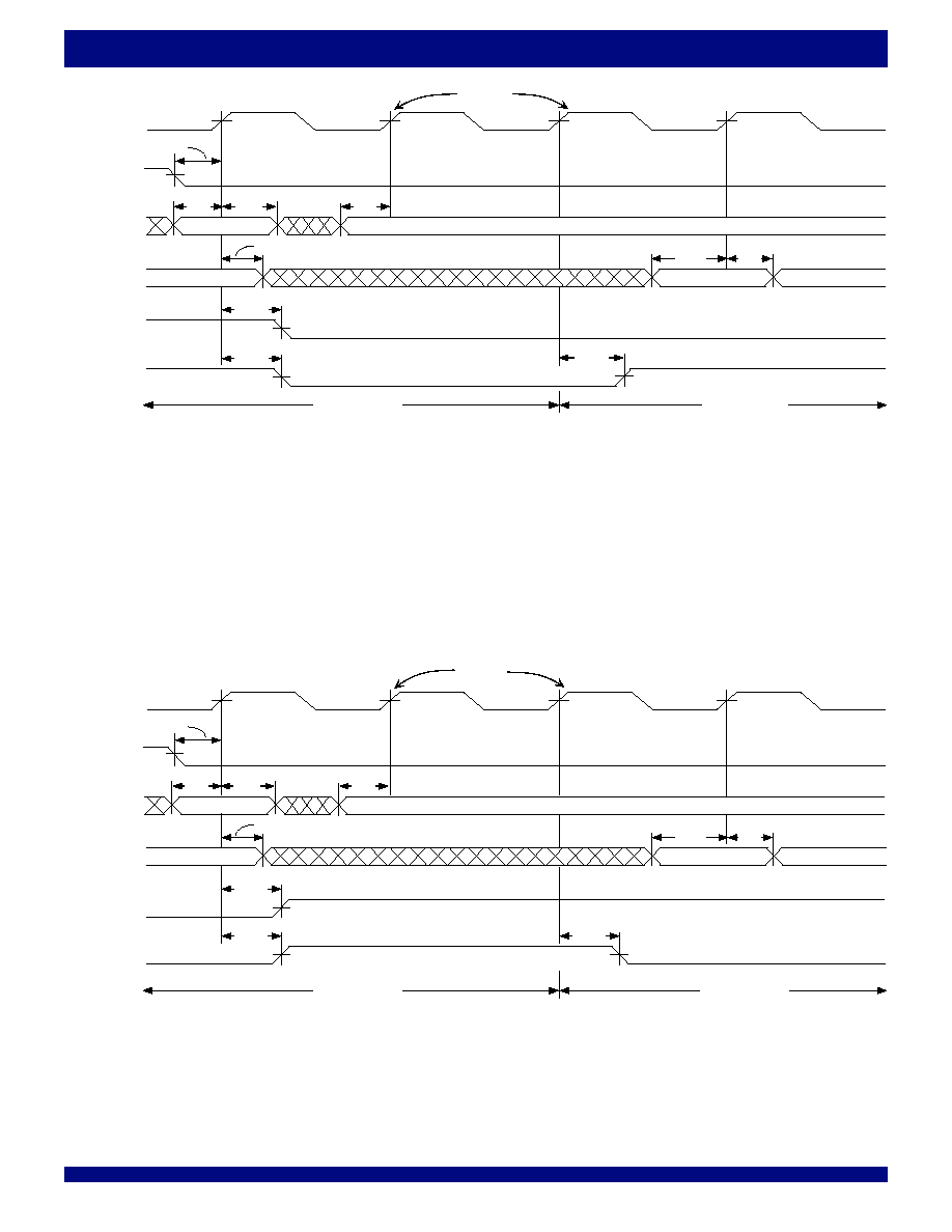
47
COMMERCIAL AND INDUSTRIAL
TEMPERATURE RANGES
IDT72T51248/72T51258/72T51268 2.5V MULTI-QUEUE DDR FLOW-CONTROL DEVICES
8,192 x 40 x 4, 16,384 x 40 x 4 and 32,768 x 40 x 4
WEN
WCLK
6159 drw32
CFF
t
WFF
t
WFF
1
2
3
IS[1:0]
01 = Queue 1
t
ENS
No Write
D[39:0]
Word D Queue 1
t
DS
t
DH
t
DH
Word A Queue 3
Word A+1 Queue 3
FF1
t
WFF
t
DS
t
DH
t
DS
11 = Queue 3
Queue 1 Status
Queue 3 Status
Figure 25. Composite Full Flag (IDT Standard mode, SDR to SDR, x40 In to x40 Out)
NOTES:
1.
WCS = LOW.
2.
FF3 is HIGH.
3. Word D is the last word written that causes Queue 1 to be full.
4. Word A is the next word written to Queue 3.
5. The composite full flag will update to the newly selected Queue after one WCLK cycle once a new Queue has been selected using IS[1:0].
WEN
WCLK
6159 drw33
CIR
t
WFF
1
2
3
IS[1:0]
t
ENS
No Write
D[39:0]
t
DH
IR1
t
WFF
Word D+1 Queue 1
t
DS
t
DH
Word A Queue 3
Word A+1 Queue 3
01 = Queue 1
t
DS
t
DH
t
DS
11 = Queue 3
t
WFF
Queue 1 Status
Queue 3 Status
Figure 26. Composite Input Ready Flag (FWFT mode, SDR to SDR, x40 In to x40 Out)
NOTES:
1.
WCS = LOW.
2.
IR3 = LOW.
3. Word D+1 is the last word written that causes Queue 1 to be full. Word D fell through to the output.
4. Word A is the next word written to Queue 3.
5. The composite full flag will update to the newly selected Queue after one WCLK cycle once a new Queue has been selected using IS[1:0].
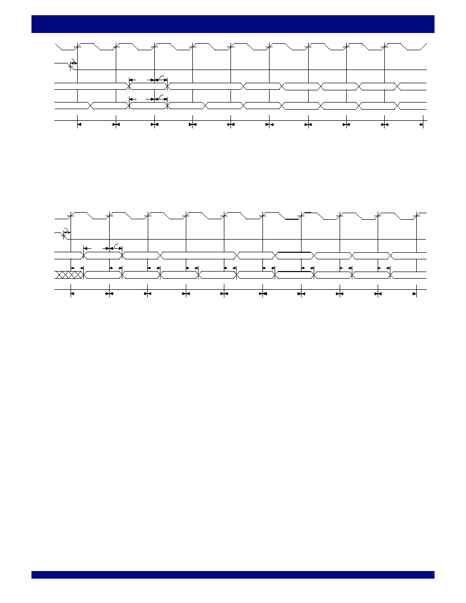
48
COMMERCIAL AND INDUSTRIAL
TEMPERATURE RANGES
IDT72T51248/72T51258/72T51268 2.5V MULTI-QUEUE DDR FLOW-CONTROL DEVICES
8,192 x 40 x 4, 16,384 x 40 x 4 and 32,768 x 40 x 4
Figure 27. Queue Switch at Every Clock Cycle (IDT Standard mode, SDR to SDR, x40 In to x40 Out)
NOTES:
1. The reading and writing to different Queues can occur at every clock cycle. There is a two cycle latency pipeline when switching from one Queue to another.
2. Word group A is written into Queue 0. Word group B Queue 1. Word group C Queue 2. Word group D Queue 3.
3. The composite empty and full flags will update the status of the newly selected Queue one cycle clock after the Queue has been selected.
4.
OE = LOW, WDDR = HIGH, and RDDR = HIGH.
5. If FWFT mode is selected, the composite input ready flag (
CIR) timing is the same as CEF. The composite output ready (COR) will update after two clock cycles instead of one.
t
A
IS[1:0]
WCLK
WEN
t
ENS
00 = Queue 0
01 = Queue 1
10 = Queue 2
11
00
D[39:0]
Word X Queue X
Word X Queue X
CFF
Queue X STATUS
t
ENS
00 = Queue 0
01 = Queue 1
10 = Queue 2
11 = Queue 3
01
10
Queue X STATUS
Queue 0 STATUS
Queue 1 STATUS
Queue 2 STATUS
Queue 3 STATUS
OS[1:0]
RCLK
REN
Q[39:0]
CEF
Queue 0
t
ENH
t
DS
t
DH
t
ENS
t
ENH
t
A
Queue 0 STATUS
Queue 0 STATUS
Queue 1 STATUS
Queue 2 STATUS
01
10
11
00
01
10
Queue 3 STATUS
Queue 1 STATUS
Queue 2 STATUS
Queue 0 STATUS
Queue 2 STATUS
Queue 3 STATUS
Queue 0 STATUS
Queue 1 STATUS
t
ENS
Word A Queue 0
Word A+1 Queue 0
Word B Queue 1
Word C Queue 2
Word C+1 Queue 2
Word D Queue 3
Word A+2 Queue 0
Word B+1 Queue 1
Word X Queue X
Word E Queue 0
Word F Queue 1
Word G Queue 2
Word H Queue 3
WordH+1 Queue 3
Word F+1 Queue 1
Word G+1 Queue 2
1
2
3
Word X+1 Queue X
t
A
t
A
t
A
t
A
t
A
t
A
t
A
6159 drw34
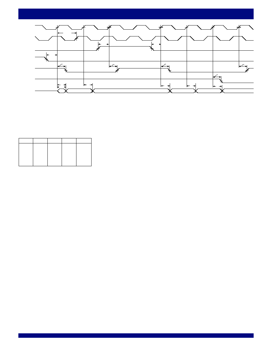
49
COMMERCIAL AND INDUSTRIAL
TEMPERATURE RANGES
IDT72T51248/72T51258/72T51268 2.5V MULTI-QUEUE DDR FLOW-CONTROL DEVICES
8,192 x 40 x 4, 16,384 x 40 x 4 and 32,768 x 40 x 4
6159 drw35
RCLK
REN
t
ERCLK
ERCLK
RCS
t
ENS
EREN
t
CLKEN
t
CLKEN
t
CLKEN
EF0
t
REF
Q[39:0]
t
OLZ
t
A
t
A
t
A
t
A
t
A
W
D-1
W
D Last Word
W
D-2
W
D-3
W
D-4
t
ENS
t
ENS
t
CLKEN
Figure 28. Echo Read Clock and Read Enable Operation (IDT Standard mode, SDR to SDR, x40 In to x40 Out)
NOTES:
1. The
EREN output is "or gated" to RCS and REN and will follow these inputs provided that the Queue is not empty. If the Queue is empty, EREN will go HIGH to indicate that
there is no new word available.
2. The
EREN output is synchronous to RCLK.
3.
OE = LOW, WDDR = HIGH, RDDR = HIGH, IS[1:0] = 00, and OS[1:0] = 00.
4. The truth table for
EREN is shown below:
RCLK
EF
RCS
REN
EREN
1
0
0
0
1
0
1
1
1
1
0
1
1
1
1
1
0
X
X
1
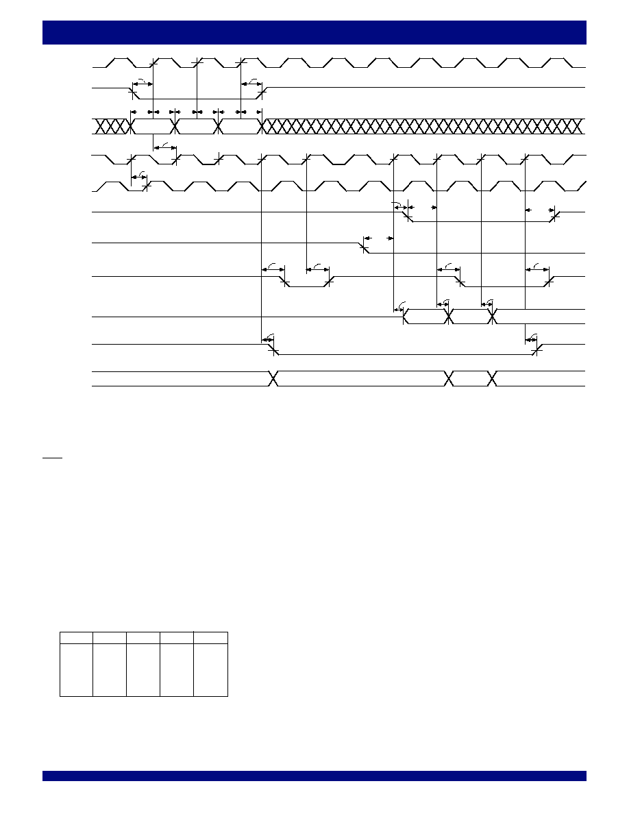
50
COMMERCIAL AND INDUSTRIAL
TEMPERATURE RANGES
IDT72T51248/72T51258/72T51268 2.5V MULTI-QUEUE DDR FLOW-CONTROL DEVICES
8,192 x 40 x 4, 16,384 x 40 x 4 and 32,768 x 40 x 4
Figure 29. Echo RCLK and Echo Read Enable Operation (FWFT mode, SDR to SDR, x40 In to x40 Out)
NOTES:
1. The O/P Register is the internal output register. Its contents are available on the Qn output bus only when
RCS and OE are both active, LOW, that is the bus is not in
High-Impedance state.
2.
OE is LOW.
Cycle:
a&b. At this point the Queue is empty,
OR0 is HIGH.
RCS and REN are both disabled, the output bus is High-Impedance.
c.
Word Wn+1 falls through to the output register,
OR0 goes active, LOW.
RCS is HIGH, therefore the Qn outputs are High-Impedance. EREN goes LOW to indicate that a new word has been placed into the output register.
d .
EREN goes HIGH, no new word has been placed into the output register on this cycle.
e.
No Operation.
f.
RCS is LOW on this cycle, therefore the Qn outputs go to Low-Impedance and the contents of the output register (Wn+1) are made available.
NOTE: In FWFT mode it's important to take
RCS active LOW at least one cycle ahead of REN, this ensures the word (Wn+1) currently in the output register is made
available for at least one cycle, otherwise Wn+1 will not be overwritten by Wn+2.
g .
REN goes active LOW, this reads out the second word, Wn+2.
EREN goes active LOW to indicate a new word has been placed into the output register.
h .
Word Wn+3 is read out,
EREN remains active, LOW indicating a new word has been read out.
NOTE: Wn+3 is the last word in the Queue.
i .
This is the next enabled read after the last word, Wn+3 has been read out.
OR0 flag goes HIGH and EREN goes HIGH to indicate that there is no new word available.
4.
OE = LOW, WDDR = LOW, RDDR = LOW, IS[1:0] = 00, and OS[1:0] = 00.
5. The truth table for
EREN is shown below:
Q[39:0]
O/P
(1)
Reg.
t
A
t
REF
OR0
6159 drw36
t
RCSLZ
REN
t
ENS
t
ENH
RCS
t
ENS
RCLK
a
b
c
d
e
f
g
h
i
W
n+1
WCLK
WEN
D[39:0]
t
SKEW1
t
ENS
t
DS
t
ENH
W
n+2
W
n+3
ERCLK
EREN
t
CLKEN
t
CLKEN
t
CLKEN
t
CLKEN
W
n+1
W
n+2
W
n+3
t
A
t
REF
W
n+1
W
n+2
W
n+3
W
n
Last Word
t
DH
t
DH
t
DH
t
DS
t
DS
1
2
t
ERCLK
HIGH-Z
t
ENH
RCLK
OR
RCS
REN
EREN
0
0
0
0
0
0
1
1
0
1
0
1
0
1
1
1
1
X
X
1

51
COMMERCIAL AND INDUSTRIAL
TEMPERATURE RANGES
IDT72T51248/72T51258/72T51268 2.5V MULTI-QUEUE DDR FLOW-CONTROL DEVICES
8,192 x 40 x 4, 16,384 x 40 x 4 and 32,768 x 40 x 4
Figure 30. Echo Read Clock and Read Enable Operation (IDT Standard mode, DDR to DDR, x10 In to x10 Out)
NOTES:
1
.
The
EREN
output is "or gated" to
RCS
and
REN
and will follow these inputs provided that the Queue is not empty. If the Queue is empty,
EREN
will go HIGH to indicate that there is no new word available.
2
.
The
EREN
output is synchronous to RCLK.
3.
OE
= LOW, WDDR = HIGH, RDDR = HIGH, IS[1:0] = 00, and OS[1:0] = 00.
4
.
The truth table for
EREN
is shown below:
EREN
EF
0
t
REF
Q[39:0]
t
CLKEN
t
CLKEN
t
OLZ
t
A
t
A
t
CLKEN
t
A
t
OLZ
t
OLZ
t
A
t
A
t
A
t
A
t
A
W
D-10
W
D-9
W
D-8
W
D-6
W
D-5
W
D-4
W
D-3
W
D-2
Last Word W
D
6159 drw37
t
A
W
D-7
W
D-6
t
A
W
D-1
RCLK
REN
ERCLK
RCS
t
ENS
t
ERCLK
t
ENH
t
ENS
t
ENH
t
CLKEN
t
CLKEN
t
CLKEN
t
ENS
NO Read
NO Read
t
ENS
RCLK
E
F
R
C
S
R
E
N
EREN
10
00
10
11
11
01
11
11
0X
X1
52
COMMERCIAL AND INDUSTRIAL
TEMPERATURE RANGES
IDT72T51248/72T51258/72T51268 2.5V MULTI-QUEUE DDR FLOW-CONTROL DEVICES
8,192 x 40 x 4, 16,384 x 40 x 4 and 32,768 x 40 x 4
Figure 31. Loading of Programmable Flag Registers (IDT Standard and FWFT modes)
t
SENH
t
SDH
SCLK
SWEN
FWFT/SI
6159 drw38
EMPTY OFFSET 3
FULL OFFSET 3
t
SENS
t
SDS
BIT
X
(1)
8
BIT 1
t
SCL
K
t
SCKH
t
SCKL
BIT 1
(
L
SB)
EMPTY OFFSET 0
FULL OFFSET 0
BIT 1
BIT 1
(
L
SB)
BIT
X
(1)
8
BIT
X
(1)
8
BIT
X
(1)
8
(
MSB)
(
MSB)
Figure 32. Reading of Programmable Flag Registers (IDT Standard and FWFT modes)
SCLK
SREN
SDO
6159 drw39
EMPTY OFFSET 3
FULL OFFSET 3
t
SENS
t
SOA
t
SEN
H
BIT X
(1)
t
SENH
t
SCLK
t
SCKH
t
SCKL
BIT 0
BIT 0
BIT X
(1)
BIT X
(1)
t
SOA
BIT 0
EMPTY OFFSET 0
FULL OFFSET 0
BIT 0
(
L
SB)
BIT X
(1)
(
MSB)
(
L
SB)
(
MSB)
NOTE:
1
.
If IW/OW = x40, X = 104 for the IDT72T51248, X = 112 for the IDT72T51258, X = 120 for the IDT72T51268.
If IW/OW = x20, X = 112 for the IDT72T51248, X = 120 for the IDT72T51258, X = 128 for the IDT72T51268.
If IW/OW = x10, X = 120 for the IDT72T51248, X = 128 for the IDT72T51258, X = 136 for the IDT72T51268.

53
COMMERCIAL AND INDUSTRIAL
TEMPERATURE RANGES
IDT72T51248/72T51258/72T51268 2.5V MULTI-QUEUE DDR FLOW-CONTROL DEVICES
8,192 x 40 x 4, 16,384 x 40 x 4 and 32,768 x 40 x 4
WCLK
WEN
PAF0
RCLK
REN
6159 drw40
1
2
1
2
D - m0 words in Queue
(1)
D - (m0 +1) words in Queue
(1)
t
ENH
t
ENS
t
PAFS
t
ENS
t
ENH
t
CLKL
t
SKEW2
(3)
t
PAFS
t
CLKL
WCLK
WEN
PAE0
RCLK
1
2
1
2
REN
6159 drw41
n0 words in Queue
t
ENS
t
SKEW2
(4)
t
ENH
t
PAES
n0 + 1 words in Queue
(2)
,
n0 + 2 words in Queue
(3)
t
ENS
t
ENH
t
CLKH
t
CLKL
NOTES:
1. m0 =
PAF0 offset .
2. D = maximum Queue depth. For density of Queue with bus-matching, refer to the bus-matching section pages 17-20.
3. t
SKEW2
is the minimum time between a rising RCLK edge and a rising WCLK edge to guarantee that
PAF0 will go HIGH (after one WCLK cycle plus t
PAFS
). If the time
between the rising edge of RCLK and the rising edge of WCLK is less than t
SKEW2
, then the
PAF0 deassertion time may be delayed one extra WCLK cycle.
4.
PAF0 is asserted and updated on the rising edge of WCLK only.
5.
RCS = LOW, WCS = LOW, WDDR = LOW, RDDR = LOW, IS[1:0] = 00, and OS[1:0] = 00.
Figure 33. Synchronous Programmable Almost-Full Flag Timing (IDT Standard and FWFT mode, SDR to SDR, x40 In to x40 Out)
NOTES:
1. n0 =
PAE0 offset.
2. For IDT Standard mode
3. For FWFT mode.
4. t
SKEW2
is the minimum time between a rising WCLK edge and a rising RCLK edge to guarantee that
PAE will go HIGH (after one RCLK cycle plus t
PAES
). If the time between
the rising edge of WCLK and the rising edge of RCLK is less than t
SKEW2
, then the
PAE0 deassertion may be delayed one extra RCLK cycle.
5.
PAE0 is asserted and updated on the rising edge of WCLK only.
6.
RCS = LOW, WCS = LOW, WDDR = LOW, RDDR = LOW, IS[1:0] = 00, and OS[1:0] = 00.
Figure 34. Synchronous Programmable Almost-Empty Flag Timing (IDT Standard and FWFT mode, SDR to SDR, x40 In to x40 Out)

54
COMMERCIAL AND INDUSTRIAL
TEMPERATURE RANGES
IDT72T51248/72T51258/72T51268 2.5V MULTI-QUEUE DDR FLOW-CONTROL DEVICES
8,192 x 40 x 4, 16,384 x 40 x 4 and 32,768 x 40 x 4
Figure 35. Power Down Operation
6159 drw44
WCLK
WEN
D[39:0]
t
DS
t
DH
t
DH
W
D10
W
D11
t
DS
t
DH
t
DS
W
D13
RCLK
REN
t
A
t
A
t
A
t
ERCLK
t
PDHZ
(7)
t
PDLZ
(2)
t
PDL
t
PDH
(2)
t
PDH
(2)
W
DH
(8)
Hi-Z
Hi-Z
W
D4
W
D3
W
D2
W
D1
Hi-Z
t
EREN
Q[39:0]
PD
ERCLK
EREN
1
2
3
4
(1)
t
DS
1
Ķs
t
A
t
EREN
W
DS
W
D12
NOTES:
1. All read and write operations must have ceased a minimum of 4 WCLK and 4 RCLK cycles before power down is asserted.
2. When the
PD input becomes deasserted, there will be a 1
Ķs waiting period before read and write operations can resume.
All input and output signals will also resume after this time period.
3. Set-up and configuration static inputs are not affected during power down.
4. Serial programming and JTAG programming port are inactive during power down.
5.
RCS = 0, WCS = 0 and OE = 0. These signals can toggle during and after power down.
6. All flags remain active and maintain their current states.
7. During power down, all outputs will be in high-impedance.
8. WDH = WD4 before power down.

55
CORPORATE HEADQUARTERS
for SALES:
for Tech Support:
2975 Stender Way
800-345-7015 or 408-727-6116
408-330-1533
Santa Clara, CA 95054
fax: 408-492-8674
email: Flow-Controlhelp@idt.com
www.idt.com
Plastic Ball Grid Array (PBGA, BB324-1)
Commercial (0
įC to +70įC)
Industrial (-40
įC to +85įC)
Low Power
6159drw45
Commercial and Industrial
Commercial and Industrial
IDT
XXXXX
Device Type
X
Power
XX
Speed
X
Package
X
Process /
Temperature
Range
BLANK
I
(1)
72T51248
8,192 x 40 x 4
2.5V Multi-Queue DDR Flow-Control Device
72T51258
16,384 x 40 x 4
2.5V Multi-Queue DDR Flow-Control Device
72T51268
32,768 x 40 x 4
2.5V Multi-Queue DDR Flow-Control Device
Clock Cycle Time (t
CLK
)
Speed in Nanoseconds
BB
5
6-7
L
ORDERING INFORMATION
NOTE:
1. Industrial temperature range product for the 5ns and 6-7 speed grades are available as a standard device.