 | –≠–Ľ–Ķ–ļ—ā—Ä–ĺ–Ĺ–Ĺ—č–Ļ –ļ–ĺ–ľ–Ņ–ĺ–Ĺ–Ķ–Ĺ—ā: 72T51356 | –°–ļ–į—á–į—ā—Ć:  PDF PDF  ZIP ZIP |
1
2003 Integrated Device Technology, Inc. All rights reserved. Product specifications subject to change without notice.
DSC-5998/2
JUNE 2003
2.5V MULTI-QUEUE FLOW-CONTROL DEVICES
(32 QUEUES) 36 BIT WIDE CONFIGURATION
1,179,648 bits
2,359,296 bits
IDT and the IDT logo are registered trademarks of Integrated Device Technology, Inc
COMMERCIAL AND INDUSTRIAL TEMPERATURE RANGES
PRELIMINARY
IDT72T51546
IDT72T51556
FEATURES:
∑
∑
∑
∑
∑
Choose from among the following memory density options:
IDT72T51546
Total Available Memory = 1,179,648 bits
IDT72T51556
Total Available Memory = 2,359,296 bits
∑
∑
∑
∑
∑
Configurable from 1 to 32 Queues
∑
∑
∑
∑
∑
Queues may be configured at master reset from the pool of
Total Available Memory in blocks of 256 x 36
∑
∑
∑
∑
∑
Independent Read and Write access per queue
∑
∑
∑
∑
∑
User programmable via serial port
∑
∑
∑
∑
∑
User selectable I/O: 2.5V LVTTL, 1.5V HSTL, 1.8V eHSTL
∑
∑
∑
∑
∑
Default multi-queue device configurations
≠ IDT72T51546 : 1,024 x 36 x 32Q
≠ IDT72T51556 : 2,048 x 36 x 32Q
∑
∑
∑
∑
∑
100% Bus Utilization, Read and Write on every clock cycle
∑
∑
∑
∑
∑
200 MHz High speed operation (5ns cycle time)
∑
∑
∑
∑
∑
3.6ns access time
∑
∑
∑
∑
∑
Echo Read Enable & Echo Read Clock Outputs
∑
∑
∑
∑
∑
Individual, Active queue flags (
OV, FF, PAE, PAF, PR)
∑
∑
∑
∑
∑
8 bit parallel flag status on both read and write ports
∑
∑
∑
∑
∑
Shows
PAE and PAF status of 8 Queues
∑
∑
∑
∑
∑
Direct or polled operation of flag status bus
∑
∑
∑
∑
∑
Global Bus Matching - (All Queues have same Input Bus Width
and Output Bus Width)
∑
∑
∑
∑
∑
User Selectable Bus Matching Options:
≠ x36in to x36out
≠ x18in to x36out
≠ x9in to x36out
≠ x36in to x18out
≠ x36in to x9out
∑
∑
∑
∑
∑
FWFT mode of operation on read port
∑
∑
∑
∑
∑
Packet mode operation
∑
∑
∑
∑
∑
Partial Reset, clears data in single Queue
∑
∑
∑
∑
∑
Expansion of up to 8 multi-queue devices in parallel is available
∑
∑
∑
∑
∑
Power Down Input provides additional power savings in HSTL
and eHSTL modes.
∑
∑
∑
∑
∑
JTAG Functionality (Boundary Scan)
∑
∑
∑
∑
∑
Available in a 256-pin PBGA, 1mm pitch, 17mm x 17mm
∑
∑
∑
∑
∑
HIGH Performance submicron CMOS technology
∑
∑
∑
∑
∑
Industrial temperature range (-40įC to +85įC) is available
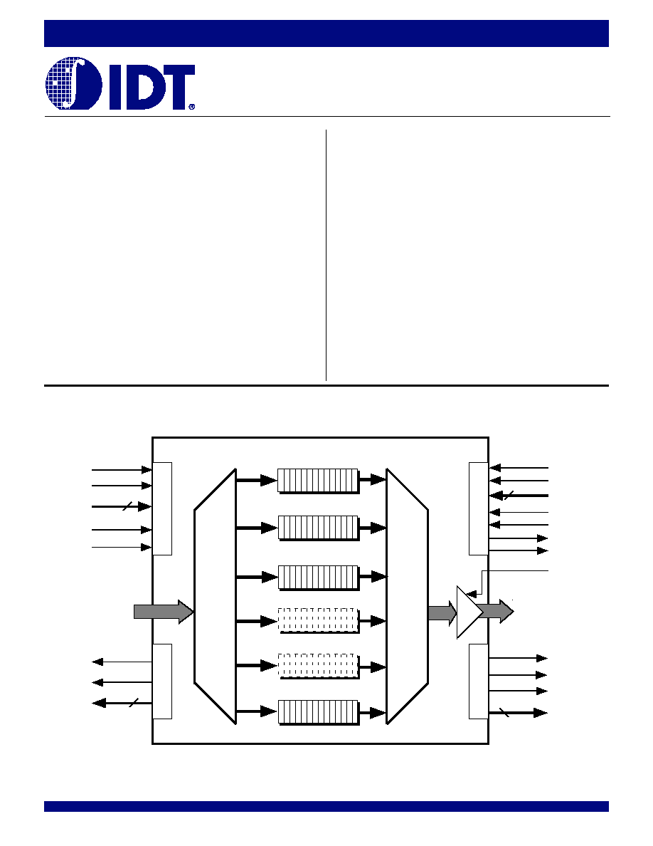
Q0
Q1
Q2
Q31
MULTI-QUEUE FLOW-CONTROL DEVICE
FSTR
WEN
PAF
FF
WRADD
WADEN
WCLK
PAFn
x36
DATA IN
ESTR
EREN
PAE
PR
RDADD
RADEN
ERCLK
PAEn
x36
DATA OUT
OE
OV
WRITE CONTROL
Din
Qout
PRn
8
8
8
8
READ CONTROL
WRITE FLAGS
READ FLAGS
5998 drw01
REN
RCLK
FUNCTIONAL BLOCK DIAGRAM

2
COMMERCIAL AND INDUSTRIAL
TEMPERATURE RANGES
IDT72T51546/72T51556 2.5V, MULTI-QUEUE FLOW-CONTROL DEVICES
(32 QUEUES) 36 BIT WIDE CONFIGURATION 1,179,648 and 2,359,296 bits
DESCRIPTION:
The IDT72T51546/72T51556 multi-queue flow-control devices is a single
chip within which anywhere between 1 and 32 discrete FIFO queues can be
setup. All queues within the device have a common data input bus, (write port)
and a common data output bus, (read port). Data written into the write port is
directed to a respective queue via an internal de-multiplex operation, ad-
dressed by the user. Data read from the read port is accessed from a respective
queue via an internal multiplex operation, addressed by the user. Data writes
and reads can be performed at high speeds up to 200MHz, with access times
of 3.6ns. Data write and read operations are totally independent of each other,
a queue maybe selected on the write port and a different queue on the read
port or both ports may select the same queue simultaneously.
The device provides Full flag and Output Valid flag status for the queue
selected for write and read operations respectively. Also a Programmable
Almost Full and Programmable Almost Empty flag for each queue is provided.
Two 8 bit programmable flag busses are available, providing status of queues
not selected for write or read operations. When 8 or less queues are configured
in the device these flag busses provide an individual flag per queue, when
more than 8 queues are used, either a Polled or Direct mode of bus operation
provides the flag busses with all queues status.
Bus Matching is available on this device, either port can be 9 bits, 18 bits
or 36 bits wide provided that at least one port is 36 bits wide. When Bus Matching
is used the device ensures the logical transfer of data throughput in a Little
Endian manner.
A packet mode of operation is also provided when the device is configured
for 36 bit input and 36 bit output port sizes. The Packet mode provides the user
with a flag output indicating when at least one (or more) packets of data within
a queue is available for reading. The Packet Ready provides the user with
a means by which to mark the start and end of packets of data being passed
through the queues. The multi-queue device then provides the user with an
internally generated packet ready status per queue.
The user has full flexibility configuring queues within the device, being able
to program the total number of queues between 1 and 32, the individual queue
depths being independent of each other. The programmable flag positions are
also user programmable. All programming is done via a dedicated serial port.
If the user does not wish to program the multi-queue device, a default option is
available that configures the device in a predetermined manner.
Both Master Reset and Partial Reset pins are provided on this device. A Master
Reset latches in all configuration setup pins and must be performed before
programming of the device can take place. A Partial Reset will reset the read and
write pointers of an individual queue, provided that the queue is selected on both
the write port and read port at the time of partial reset.
Echo Read Enable,
EREN and Echo Read Clock, ERCLK outputs are
provided. These are outputs from the read port of the Queue that are required
for high speed data communication, to provide tighter synchronization between
the data being transmitted from the Qn outputs and the data being received by
the input device. Data read from the read port is available on the output bus with
respect to
EREN and ERCLK, this is very useful when data is being read at high
speed.
The multi-queue flow-control device has the capability of operating its IO in
either 2.5V LVTTL, 1.5V HSTL or 1.8V eHSTL mode. The type of IO is selected
via the IOSEL input. The core supply voltage (V
CC
) to the multi-queue is always
2.5V, however the output levels can be set independently via a separate supply,
V
DDQ
.
The devices also provide additional power savings via a Power Down Input.
This input disables the write port data inputs when no write operations are
required.
A JTAG test port is provided, here the multi-queue flow-control device has a
fully functional Boundary Scan feature, compliant with IEEE 1149.1 Standard
Test Access Port and Boundary Scan Architecture.
See Figure 1, Multi-Queue Flow-Control Device Block Diagram for an outline
of the functional blocks within the device.
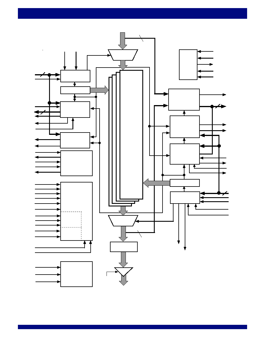
3
IDT72T51546/72T51556 2.5V, MULTI-QUEUE FLOW-CONTROL DEVICES
(32 QUEUES) 36 BIT WIDE CONFIGURATION 1,179,648 and 2,359,296 bits
COMMERCIAL AND INDUSTRIAL
TEMPERATURE RANGES
OE
x9, x18, x36
Qout
OUTPUT
REGISTER
Q0 - Q35
WRADD
WADEN
INPUT
DEMUX
WCLK
WEN
Write Control
Logic
Din
Write Pointers
Active Q
Flags
PAF
General Flag
Monitor
FSTR
PAFn
FF
FSYNC
PAF
Reset
Logic
Serial
Multi-Queue
Program-
ming
PAE/ PAF
Offset
TMS
TDI
TDO
TCK
TRST
FM
IW
OW
BM
PRS
MRS
SI
SO
SCLK
SENI
RCLK
REN
Read Control
Logic
Read Pointers
Active Q
Flags
PAE
General Flag
Monitor
ESTR
OV
ESYNC
RDADD
RADEN
DF
FXO
FXI
EXI
EXO
5998 drw02
x9, x18, x36
8
8
8
ID0
ID1
ID2
Device ID
3 Bit
PKT
Packet
Mode Logic
JTAG
Logic
D35 = TEOP
D34 = TSOP
2
Q35 = REOP
Q34 = RSOP
2
PR
PRn/PAEn
8
SENO
DFM
MAST
PAE
Upto 32
FIFO
Queues
2.3 Mbit
Dual Port
Memory
OUTPUT
MUX
D0 - D35
NULL-Q
ERCLK
EREN
IO Level Control
&
Power Down
IOSEL
Vref
PD
Figure 1. Multi-Queue Flow-Control Device Block Diagram
4
COMMERCIAL AND INDUSTRIAL
TEMPERATURE RANGES
IDT72T51546/72T51556 2.5V, MULTI-QUEUE FLOW-CONTROL DEVICES
(32 QUEUES) 36 BIT WIDE CONFIGURATION 1,179,648 and 2,359,296 bits
PRELIMINARY
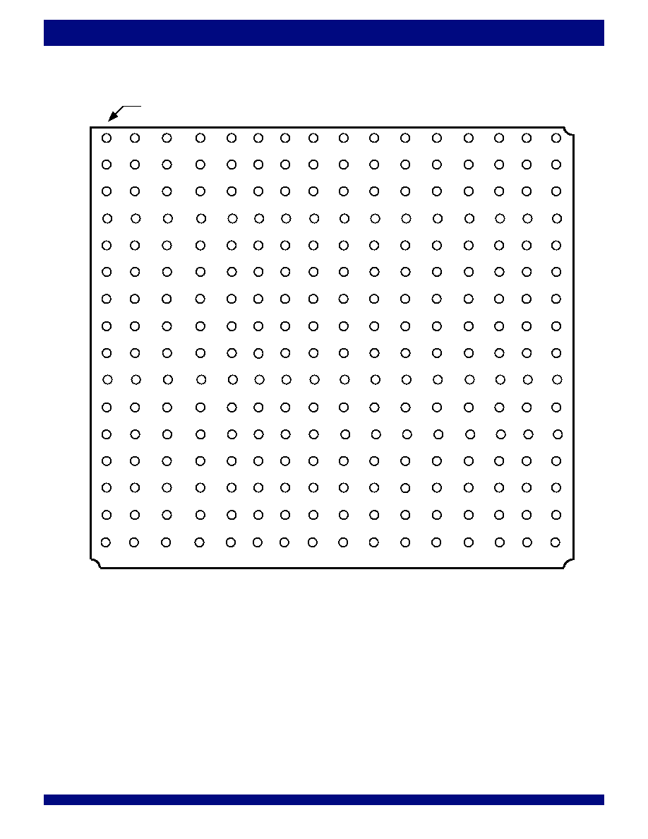
D14
A
D13
D12
D10
Q9
D7
Q6
D4
Q3
D1
ID1
TCK
TDO
Q12
Q14
Q15
D15
B
D16
D11
D9
Q8
D6
Q5
D3
Q2
D0
ID0
TMS
TDI
Q11
Q13
Q19
D17
C
D18
D19
D8
Q7
D5
Q4
D2
Q1
TRST
Q0
IOSEL
ID2
Q10
Q17
Q18
D20
D
D21
D22
V
DDQ
V
DDQ
V
DDQ
V
DDQ
V
DDQ
V
DDQ
V
CC
V
CC
V
CC
V
CC
Q16
Q21
Q20
D23
E
D24
D25
V
DDQ
V
DDQ
V
DDQ
V
DDQ
V
CC
V
CC
V
CC
V
CC
GND
GND
Q24
Q23
Q22
D26
F
D27
D28
V
DDQ
V
DDQ
V
CC
V
CC
GND
GND
GND
GND
GND
GND
Q27
Q26
Q25
D29
G
D30
D31
V
CC
V
CC
V
CC
V
CC
GND
GND
GND
GND
GND
GND
Q30
Q29
Q28
D32
H
D33
D34
V
CC
V
CC
GND
GND
GND
GND
GND
GND
GND
GND
Q33
Q32
Q31
GND
J
NULL-Q
D35
V
CC
V
CC
GND
GND
GND
GND
GND
GND
GND
GND
PKT
Q35
Q34
PD
K
GND
VREF
V
CC
V
CC
V
CC
V
CC
GND
GND
GND
GND
GND
GND
GND
MAST
FM
SI
L
DFM
DF
V
DDQ
V
DDQ
V
CC
V
CC
GND
GND
GND
GND
GND
GND
BM
IW
OW
SENO
M
SENI
SO
V
DDQ
V
DDQ
V
DDQ
V
DDQ
V
CC
V
CC
V
CC
V
CC
GND
GND
OE
RDADD0 RDADD1
WRADD1
N
WRADD0
SCLK
V
DDQ
V
DDQ
V
DDQ
V
DDQ
V
DDQ
V
DDQ
V
CC
V
CC
V
CC
V
CC
RDADD2 RDADD3 RDADD4
WRADD4
P
WRADD3 WRADD2
WADEN
PAE3
PAF3
PAE6
PAF6
PAE7
PAF7
PAE
FF
OV
RDADD5 RDADD6 RDADD7
WRADD6
R
WRADD5 FSYNC
FSTR
PAE2
PAF2
PAE5
PAF5
EREN
PAF4
ERCLK
PAF
PR
RADEN
ESTR
ESYNC
WRADD7
T
FXI
FXO
PAF0
PAE1
PAF1
PAE4
WEN
REN
WCLK
RCLK
PRS
MRS
PAE0
1
2
3
4
13
5
12
6
11
7
10
8
9
14
15
16
5998 drw03
A1 BALL PAD CORNER
EXO
EXI
PIN CONFIGURATION
PBGA (BB256-1, order code: BB)
TOP VIEW

5
IDT72T51546/72T51556 2.5V, MULTI-QUEUE FLOW-CONTROL DEVICES
(32 QUEUES) 36 BIT WIDE CONFIGURATION 1,179,648 and 2,359,296 bits
COMMERCIAL AND INDUSTRIAL
TEMPERATURE RANGES
DETAILED DESCRIPTION
MULTI-QUEUE STRUCTURE
The IDT multi-queue flow-control device has a single data input port and
single data output port with up to 32 FIFO queues in parallel buffering between
the two ports. The user can setup between 1 and 32 Queues within the device.
These queues can be configured to utilize the total available memory, providing
the user with full flexibility and ability to configure the queues to be various depths,
independent of one another.
MEMORY ORGANIZATION/ ALLOCATION
The memory is organized into what is known as "blocks", each block being
256 x36 bits. When the user is configuring the number of queues and individual
queue sizes the user must allocate the memory to respective queues, in units
of blocks, that is, a single queue can be made up from 0 to m blocks, where m
is the total number of blocks available within a device. Also the total size of any
given queue must be in increments of 256 x36. For the IDT72T51546 and
IDT72T51556 the Total Available Memory is 128 and 256 blocks respectively
(a block being 256 x36). Queues can be built from these blocks to make any
size queue desired and any number of queues desired.
BUS WIDTHS
The input port is common to all queues within the device, as is the output port.
The device provides the user with Bus Matching options such that the input port
and output port can be either x9, x18 or x36 bits wide provided that at least one
of the ports is x36 bits wide, the read and write port widths being set
independently of one another. Because the ports are common to all queues the
width of the queues is not individually set, so that the input width of all queues
are equal and the output width of all queues are equal.
WRITING TO & READING FROM THE MULTI-QUEUE
Data being written into the device via the input port is directed to a discrete
queue via the write queue select address inputs. Conversely, data being read
from the device read port is read from a queue selected via the read queue select
address inputs. Data can be simultaneously written into and read from the same
queue or different queues. Once a queue is selected for data writes or reads,
the writing and reading operation is performed in the same manner as a
conventional IDT synchronous FIFO, utilizing clocks and enables, there is a
single clock and enable per port. When a specific queue is addressed on the
write port, data placed on the data inputs is written to that queue sequentially
based on the rising edge of a write clock provided setup and hold times are met.
Conversely, data is read on to the output port after an access time from a rising
edge on a read clock.
The operation of the write port is comparable to the function of a conventional
FIFO operating in standard IDT mode. Write operations can be performed on
the write port provided that the queue currently selected is not full, a full flag output
provides status of the selected queue. The operation of the read port is
comparable to the function of a conventional FIFO operating in FWFT mode.
When a queue is selected on the output port, the next word in that queue will
automatically fall through to the output register. All subsequent words from that
queue require an enabled read cycle. Data cannot be read from a selected
queue if that queue is empty, the read port provides an Output Valid flag indicating
when data read out is valid. If the user switches to a queue that is empty, the
last word from the previous queue will remain on the output register.
As mentioned, the write port has a full flag, providing full status of the selected
queue. Along with the full flag a dedicated almost full flag is provided, this almost
full flag is similar to the almost full flag of a conventional IDT FIFO. The device
provides a user programmable almost full flag for all 32 queues and when a
respective queue is selected on the write port, the almost full flag provides status
for that queue. Conversely, the read port has an output valid flag, providing
status of the data being read from the queue selected on the read port. As well
as the output valid flag the device provides a dedicated almost empty flag. This
almost empty flag is similar to the almost empty flag of a conventional IDT FIFO.
The device provides a user programmable almost empty flag for all 32 queues
and when a respective queue is selected on the read port, the almost empty flag
provides status for that queue.
PROGRAMMABLE FLAG BUSSES
In addition to these dedicated flags, full & almost full on the write port and output
valid & almost empty on the read port, there are two flag status busses. An almost
full flag status bus is provided, this bus is 8 bits wide. Also, an almost empty flag
status bus is provided, again this bus is 8 bits wide. The purpose of these flag
busses is to provide the user with a means by which to monitor the data levels
within queues that may not be selected on the write or read port. As mentioned,
the device provides almost full and almost empty registers (programmable by
the user) for each of the 32 queues in the device.
In the IDT72T51546/72T51556 multi-queue flow-control devices the user
has the option of utilizing anywhere between 1 and 32 queues, therefore the
8 bit flag status busses are multiplexed between the 32 queues, a flag bus can
only provide status for 8 of the 32 queues at any moment, this is referred to as
a "Quadrant", such that when the bus is providing status of queues 1 through
8, this is quadrant 1, when it is queues 9 through 16, this is quadrant 2 and so
on up to quadrant 4. If less than 32 queues are setup in the device, there are
still 4 quadrants, such that in "Polled" mode of operation the flag bus will still cycle
through 4 quadrants. If for example only 22 queues are setup, quadrants 1 and
2 will reflect status of queues 1 through 8 and 9 through 16 respectively.
Quadrant 3 will reflect the status of queues 17 through 22 on the least significant
6 bits, the most significant 2 bits of the flag bus are don't care and the 4th quadrant
outputs will be don't care also.
The flag busses are available in two user selectable modes of operation,
"Polled" or "Direct". When operating in polled mode a flag bus provides status
of each quadrant sequentially, that is, on each rising edge of a clock the flag bus
is updated to show the status of each quadrant in order. The rising edge of the
write clock will update the almost full bus and a rising edge on the read clock will
update the almost empty bus. The mode of operation is always the same for both
the almost full and almost empty flag busses. When operating in direct mode, the
quadrant on the flag bus is selected by the user. So the user can actually address
the quadrant to be placed on the flag status busses, these flag busses operate
independently of one another. Addressing of the almost full flag bus is done via
the write port and addressing of the almost empty flag bus is done via the read
port.
PACKET READY
The multi-queue flow-control device also offers a "Packet Mode" operation.
Packet Mode is user selectable and requires the device to be configured with
both write and read ports as 36 bits wide. In packet mode, users can define the
length of packets or frame by using the two most significant bits of the 36-bit word.
Bit 34 is used to mark the Start of Packet (SOP) and bit 35 is used to mark the
End of Packet (EOP) as shown in Table 5). When writing data into a given queue
, the first word being written is marked, by the user setting bit 34 as the "Start
of Packet" (SOP) and the last word written is marked as the "End of Packet" (EOP)
with all words written between the Start of Packet (SOP) marker (bit 34) and the
End of packet (EOP) packet marker (bit 35) constituting the entire packet. A
packet can be any length the user desires, up to the total available memory in
the multi-queue device. The device monitors the SOP (bit 34) and looks for the
word that contains the EOP (bit 35). The read port is supplied with an additional

6
COMMERCIAL AND INDUSTRIAL
TEMPERATURE RANGES
IDT72T51546/72T51556 2.5V, MULTI-QUEUE FLOW-CONTROL DEVICES
(32 QUEUES) 36 BIT WIDE CONFIGURATION 1,179,648 and 2,359,296 bits
status flag, "Packet Ready". The Packet Ready (
PR) flag in conjunction with
Output Valid (
OV) indicates when at least one packet is available to read. When
in packet mode the almost empty flag status , provides packet ready flag status
for individual queues.
EXPANSION
Expansion of multi-queue devices is also possible, up to 8 devices can be
connected in a parallel fashion providing the possibility of both depth expansion
or queue expansion. Depth Expansion means expanding the depths of
individual queues. Queue expansion means increasing the total number of
queues available. Depth expansion is possible by virtue of the fact that more
memory blocks within a multi-queue device can be allocated to increase the
depth of a queue. For example, depth expansion of 8 devices provides the
possibility of 8 queues of 64K x36 deep, each queue being setup within a single
device utilizing all memory blocks available to produce a single queue. This is
the deepest queue that can setup within a device.
For queue expansion a maximum number of 256 (8 x 32) queues may be
setup, each queue being 2K x36 deep, if less queues are setup, then more
memory blocks will be available to increase queue depths if desired. When
connecting multi-queue devices in expansion mode all respective input pins
(data & control) and output pins (data & flags), should be "connected" together
between individual devices.

7
IDT72T51546/72T51556 2.5V, MULTI-QUEUE FLOW-CONTROL DEVICES
(32 QUEUES) 36 BIT WIDE CONFIGURATION 1,179,648 and 2,359,296 bits
COMMERCIAL AND INDUSTRIAL
TEMPERATURE RANGES
BM
Bus Matching
LVTTL
This pin is setup before Master Reset and must not toggle during any device operation. This pin is used
(L14)
INPUT
along with IW and OW to setup the multi-queue flow-control device bus width. Please refer to Table 3
for details.
D[35:0]
Data Input Bus
HSTL-LVTTL These are the 36 data input pins. Data is written into the device via these input pins on the rising edge
Din
INPUT
of WCLK provided that
WEN is LOW. Note, that in Packet mode D32-D35 may be used as packet
(See Pin No.
markers, please see packet ready functional discussion for more detail. Due to bus matching not all inputs
table for details)
may be used, any unused inputs should be tied LOW.
DF
(1)
Default Flag
LVTTL
If the user requires default programming of the multi-queue device, this pin must be setup before Master
(L3)
INPUT
Reset and must not toggle during any device operation. The state of this input at master reset determines
the value of the
PAE/PAF flag offsets. If DF is LOW the value is 8, if DF is HIGH the value is 128.
DFM
(1)
Default Mode
LVTTL
The multi-queue device requires programming after master reset. The user can do this serially via the
(L2)
INPUT
serial port, or the user can use the default method. If DFM is LOW at master reset then serial mode will be
selected, if HIGH then default mode is selected.
ERCLK
RCLK Echo
HSTL-LVTTL Read Clock Echo output, this output generates a clock based on the read clock input, this is used for Source
(R10)
OUTPUT
Synchronous clocking where the receiving devices utilizes the ERCLK to clock data output from the Queue.
EREN
REN Echo
HSTL-LVTTL Read Enable Echo output, can be used in conjunction with the ERCLK output to load data output from the
(R11)
OUTPUT
Queue into the receiving device.
ESTR
PAEn Flag Bus
LVTTL
If direct operation of the
PAEn bus has been selected, the ESTR input is used in conjunction with RCLK
(R15)
Strobe
INPUT
and the RDADD bus to select a quadrant of queues to be placed on to the
PAEn bus outputs. A quadrant
addressed via the RDADD bus is selected on the rising edge of RCLK provided that ESTR is HIGH. If
Polled operations has been selected, ESTR should be tied inactive, LOW. Note, that a
PAEn flag bus
selection cannot be made, (ESTR must NOT go active) until programming of the part has been completed
and
SENO has gone LOW.
ESYNC
PAEn Bus Sync HSTL-LVTTL ESYNC is an output from the multi-queue device that provides a synchronizing pulse for the PAEn bus
(R16)
OUTPUT
during Polled operation of the
PAEn bus. During Polled operation each quadrant of queue status flags is
loaded on to the
PAEn bus outputs sequentially based on RCLK. The first RCLK rising edge loads
quadrant 1 on to
PAEn, the second RCLK rising edge loads quadrant 2 and so on. The fifth RCLK rising
edge will again load quadrant 1. During the RCLK cycle that quadrant 1 of a selected device is placed
on to the
PAEn bus, the ESYNC output will be HIGH. For all other quadrants of that device, the ESYNC
output will be LOW.
EXI
PAEn Bus
LVTTL
The EXI input is used when multi-queue devices are connected in expansion mode and Polled
PAEn
(T16)
Expansion In
INPUT
bus operation has been selected . EXI of device `N' connects directly to EXO of device `N-1'. The EXI
receives a token from the previous device in a chain. In single device mode the EXI input must be tied
LOW if the
PAEn bus is operated in direct mode. If the PAEn bus is operated in polled mode the EXI input
must be connected to the EXO output of the same device. In expansion mode the EXI of the first device
should be tied LOW, when direct mode is selected.
EXO
PAEn Bus
LVTTL
EXO is an output that is used when multi-queue devices are connected in expansion mode and Polled
(T15)
Expansion Out
OUTPUT
PAEn bus operation has been selected . EXO of device `N' connects directly to EXI of device `N+1'. This
pin pulses when device N has placed its final (4th) quadrant on to the
PAEn bus with respect to RCLK.
This pulse (token) is then passed on to the next device in the chain `N+1' and on the next RCLK rising
edge the first quadrant of device N+1 will be loaded on to the
PAEn bus. This continues through the chain
and EXO of the last device is then looped back to EXI of the first device. The ESYNC output of each device
in the chain provides synchronization to the user of this looping event.
FF
Full Flag
HSTL-LVTTL This pin provides the full flag output for the active Queue, that is, the queue selected on the input port
(P8)
OUTPUT
for write operations, (selected via WCLK, WRADD bus and WADEN). On the WCLK cycle after a queue
selection, this flag will show the status of the newly selected queue. Data can be written to this queue on
the next cycle provided
FF is HIGH. This flag has High-Impedance capability, this is important during
expansion of devices, when the
FF flag output of up to 8 devices may be connected together on a common
line. The device with a queue selected takes control of the
FF bus, all other devices place their FF output
into High-Impedance. When a queue selection is made on the write port this output will switch from
High-Impedance control on the next WCLK cycle. This flag is synchronized to WCLK.
PIN DESCRIPTIONS
Symbol &
Name
I/O TYPE
Description
Pin No.

8
COMMERCIAL AND INDUSTRIAL
TEMPERATURE RANGES
IDT72T51546/72T51556 2.5V, MULTI-QUEUE FLOW-CONTROL DEVICES
(32 QUEUES) 36 BIT WIDE CONFIGURATION 1,179,648 and 2,359,296 bits
PIN DESCRIPTIONS (CONTINUED)
FM
(1)
Flag Mode
HSTL-LVTTL This pin is setup before a master reset and must not toggle during any device operation. The state of the
(K16)
INPUT
FM pin during Master Reset will determine whether the
PAFn and PAEn flag busses operate in either Polled
or Direct mode. If this pin is HIGH the mode is Polled, if LOW then it will be Direct.
FSTR
PAFn Flag Bus
LVTTL
If direct operation of the
PAFn bus has been selected, the FSTR input is used in conjunction with WCLK
(R4)
Strobe
INPUT
and the WRADD bus to select a quadrant of queues to be placed on to the
PAFn bus outputs. A quadrant
addressed via the WRADD bus is selected on the rising edge of WCLK provided that FSTR is HIGH. If
Polled operations has been selected, FSTR should be tied inactive, LOW. Note, that a
PAFn flag bus
selection cannot be made, (FSTR must NOT go active) until programming of the part has been completed
and
SENO has gone LOW.
FSYNC
PAFn Bus Sync
LVTTL
FSYNC is an output from the multi-queue device that provides a synchronizing pulse for the
PAFn bus
(R3)
OUTPUT
during Polled operation of the
PAFn bus. During Polled operation each quadrant of queue status flags
is loaded on to the
PAFn bus outputs sequentially based on WCLK. The first WCLK rising edge loads
quadrant 1 on to
PAFn, the second WCLK rising edge loads quadrant 2 and so on. The fifth WCLK rising
edge will again load quadrant 1. During the WCLK cycle that quadrant 1 of a selected device is placed
on to the
PAFn bus, the FSYNC output will be HIGH. For all other quadrants of that device, the FSYNC
output will be LOW.
FXI
PAFn Bus
LVTTL
The FXI input is used when multi-queue devices are connected in expansion mode and Polled
PAFn
(T2)
Expansion In
INPUT
bus operation has been selected . FXI of device `N' connects directly to FXO of device `N-1'. The FXI
receives a token from the previous device in a chain. In single device mode the FXI input must be tied
LOW if the
PAFn bus is operated in direct mode. If the PAFn bus is operated in polled mode the FXI input
must be connected to the FXO output of the same device. In expansion mode the FXI of the first device
should be tied LOW, when direct mode is selected.
FXO
PAFn Bus
LVTTL
FXO is an output that is used when multi-queue devices are connected in expansion mode and Polled
(T3)
Expansion Out
OUTPUT
PAFn bus operation has been selected . FXO of device `N' connects directly to FXI of device `N+1'. This
pin pulses when device N has placed its final (4th) quadrant on to the
PAFn bus with respect to WCLK.
This pulse (token) is then passed on to the next device in the chain `N+1' and on the next WCLK rising
edge the first quadrant of device N+1 will be loaded on to the
PAFn bus. This continues through the chain
and FXO of the last device is then looped back to FXI of the first device. The FSYNC output of each device
in the chain provides synchronization to the user of this looping event.
ID[2:0]
(1)
Device ID Pins
HSTL-LVTTL For the 32Q multi-queue device the WRADD and RDADD address busses are 8 bits wide. When a queue
ID2-C9
INPUT
selection takes place the 3 MSb's of this 8 bit address bus are used to address the specific device (the
ID1-A10
5 LSb's are used to address the queue within that device). During write/read operations the 3 MSb's
ID0-B10
of the address are compared to the device ID pins. The first device in a chain of multi-queue's (connected
in expansion mode), may be setup as `000', the second as `001' and so on through to device 8 which
is `111', however the ID does not have to match the device order. In single device mode these pins should
be setup as `000' and the 3 MSb's of the WRADD and RDADD address busses should be tied LOW. The
ID[2:0] inputs setup a respective devices ID during master reset. These ID pins must not toggle during
any device operation. Note, the device selected as the `Master' does not have to have the ID of `000'.
IOSEL
IO Select
LVTTL
This pin is used to select either HSTL or 2.5V LVTTL operation for the I/O. If HSTL or eHSTL I/O are
(C8)
INPUT
required then IOSEL should be tied HIGH. If LVTTL I/O are required then it should be tied LOW.
IW
(1)
Input Width
LVTTL
This pin is used in conjunction with OW and BM to setup the input and output bus widths to be a combination
(L15)
INPUT
of x9, x18 or x36, (providing that one port is x36).
MAST
(1)
Master Device
HSTL-LVTTL The state of this input at Master Reset determines whether a given device (within a chain of devices), is the
(K15)
INPUT
Master device or a Slave. If this pin is HIGH, the device is the master if it is LOW then it is a Slave. The
master device is the first to take control of all outputs after a master reset, all slave devices go to High-
Impedance, preventing bus contention. If a multi-queue device is being used in single device mode, this
pin must be set HIGH.
MRS
Master Reset
HSTL-LVTTL A master reset is performed by taking
MRS from HIGH to LOW, to HIGH. Device programming is required
(T9)
INPUT
after master reset.
NULL-Q
Null Queue
HSTL-LVTTL This pin is used on the read port when a Null-Q is required, it is used in conjunction with the RDADD
(J2)
Select
INPUT
and RADEN address bus to address the Null-Q.
Symbol &
Name
I/O TYPE
Description
Pin No.

9
IDT72T51546/72T51556 2.5V, MULTI-QUEUE FLOW-CONTROL DEVICES
(32 QUEUES) 36 BIT WIDE CONFIGURATION 1,179,648 and 2,359,296 bits
COMMERCIAL AND INDUSTRIAL
TEMPERATURE RANGES
OE
Output Enable
HSTL-LVTTL The Output enable signal is an Asynchronous signal used to provide three-state control of the multi-queue
(M14)
INPUT
data output bus, Qout. If a device has been configured as a "Master" device, the Qout data outputs will
be in a Low Impedance condition if the
OE input is LOW. If OE is HIGH then the Qout data outputs will be
in High Impedance. If a device is configured a "Slave" device, then the Qout data outputs will always be
in High Impedance until that device has been selected on the Read Port, at which point
OE provides three-
state of that respective device.
OV
Output Valid
HSTL-LVTTL This output flag provides output valid status for the data word present on the multi-queue flow-control device
(P9)
Flag
OUTPUT
data output port, Qout. This flag is therefore, 2-stage delayed to match the data output path delay. That
is, there is a 2 RCLK cycle delay from the time a given queue is selected for reads, to the time the
OV
flag represents the data in that respective queue. When a selected queue on the read port is read to
empty, the
OV flag will go HIGH, indicating that data on the output bus is not valid. The OV flag also has
High-Impedance capability, required when multiple devices are used and the
OV flags are tied together.
OW
(1)
Output Width
LVTTL
This pin is setup during Master Reset and must not toggle during any device operation. This pin is used
(L16)
INPUT
in conjunction with IW and BM to setup the data input and output bus widths to be a combination of x9,
x18 or x36, (providing that one port is x36).
PAE
Programmable
HSTL-LVTTL This pin provides the Almost-Empty flag status for the Queue that has been selected on the output port
(P10)
Almost-Empty
OUTPUT
for read operations, (selected via RCLK, RDADD and RADEN). This pin is LOW when the selected
Flag
Queue is almost-empty. This flag output may be duplicated on one of the
PAEn bus lines. This flag is
synchronized to RCLK.
PAEn/PRn
Programmable
HSTL-LVTTL On the 32Q device the
PAEn/PRn bus is 8 bits wide. During a Master Reset this bus is setup for either
(
PAE7-P11
Almost-Empty
OUTPUT
Almost Empty mode or Packet mode. This output bus provides
PAE/PRn status of 8 queues (1 quadrant),
PAE6-P12
Flag Bus/Packet
within a selected device, having a total of 4 quadrants. During Queue read/write operations these outputs
PAE5-R12
ReadyFlag Bus
provide programmable empty flag status or packet ready status, in either direct or polled mode. The mode
PAE4-T12
of flag operation is determined during master reset via the state of the FM input. This flag bus is capable of
PAE3-P13
High-Impedance state, this is important during expansion of multi-queue devices. During direct operation
PAE2-R13
the
PAEn/PRn bus is updated to show the PAE/PR status of a quadrant of queues within a selected device.
PAE1-T13
Selection is made using RCLK, ESTR and RDADD. During Polled operation the
PAEn/PRn bus is
PAE0-T14)
loaded with the
PAE/PRn status of multi-queue flow-control quadrants sequentially based on the rising
edge of RCLK.
PAE or PR operation is determined by the state of PKT during master reset.
PAF
Programmable
HSTL-LVTTL This pin provides the Almost-Full flag status for the Queue that has been selected on the input port for
(R8)
Almost-Full Flag
OUTPUT
write operations, (selected via WCLK, WRADD and WADEN). This pin is LOW when the selected
Queue is almost-full. This flag output may be duplicated on one of the
PAFn bus lines. This flag is
synchronized to WCLK.
PAFn
Programmable
HSTL-LVTTL On the 32Q device the
PAFn bus is 8 bits wide. At any one time this output bus provides PAF status
(
PAF7-P7
Almost-Full Flag
OUTPUT
of 8 queues (1 quadrant), within a selected device, having a total of 4 quadrants. During Queue read/
PAF6-P6
Bus
write operations these outputs provide programmable full flag status, in either direct or polled mode. The
PAF5-R6
mode of flag operation is determined during master reset via the state of the FM input. This flag bus is
PAF4-R7
capable of High-Impedance state, this is important during expansion of multi-queue devices. During direct
PAF3-P5
operation the
PAFn bus is updated to show the PAF status of a quadrant of queues within a selected
PAF2-R5
device. Selection is made using WCLK, FSTR, WRADD and WADEN. During Polled operation the
PAFn
PAF1-T5
bus is loaded with the
PAF status of multi-queue flow-control quadrants sequentially based on the rising
PAF0-T4)
edge of WCLK.
PD
Power Down
HSTL
This input is used to provide additional power savings. When the device I/O is setup for HSTL/eHSTL
(K1)
INPUT
mode a HIGH on the PD input disables the data inputs on the write port only, providing significant power
savings. In LVTTL mode this pin has no operation
PKT
(1)
Packet Mode
LVTTL
The state of this pin during a Master Reset will determine whether the part is operating in Packet mode
(J14)
INPUT
providing both a Packet Ready (
PR) output and a Programmable Almost Empty (PAE) discrete output,
or standard mode, providing a (
PAE) output only. If this pin is HIGH during Master Reset the part will
operate in packet mode, if it is LOW then almost empty mode. If packet mode has been selected the read
port flag bus becomes packet ready flag bus,
PRn and the discrete packet ready flag, PR is functional.
If almost empty operation has been selected then the flag bus provides almost empty status,
PAEn and
PIN DESCRIPTIONS (CONTINUED)
Symbol &
Name
I/O TYPE
Description
Pin No.

10
COMMERCIAL AND INDUSTRIAL
TEMPERATURE RANGES
IDT72T51546/72T51556 2.5V, MULTI-QUEUE FLOW-CONTROL DEVICES
(32 QUEUES) 36 BIT WIDE CONFIGURATION 1,179,648 and 2,359,296 bits
PIN DESCRIPTIONS (CONTINUED)
PKT
(1)
Packet Mode
LVTTL
the discrete almost empty flag,
PAE is functional, the PR flag is inactive and should not be connected.
(Continued)
INPUT
Packet Ready utilizes user marked locations to identify start and end of packets being written into the
(J14)
device. Packet Mode can only be selected if both the input port width and output port width are 36 bits.
PR
Packet Ready
HSTL-LVTTL If packet mode has been selected this flag output provides Packet Ready status of the Queue selected
(R9)
Flag
OUTPUT
for read operations. During a master reset the state of the PKT input determines whether Packet mode
of operation will be used. If Packet mode is selected, then the condition of the
PR flag and OV signal are
asserted indicates a packet is ready for reading. The user must mark the start of a packet and the end of
a packet when writing data into a queue. Using these Start Of Packet (SOP) and End Of Packet (EOP)
markers, the multi-queue device sets
PR LOW if one or more "complete" packets are available in the queue.
A complete packet(s) must be written before the user is allowed to switch queues.
PRS
Partial Reset
HSTL-LVTTL A Partial Reset can be performed on a single queue selected within the multi-queue device. Before a Partial
(T8)
INPUT
Reset can be performed on a queue, that queue must be selected on both the write port and read port
2 clock cycles before the reset is performed. A Partial Reset is then performed by taking
PRS LOW for
one WCLK cycle and one RCLK cycle. The Partial Reset will only reset the read and write pointers to
the first memory location, none of the devices configuration will be changed.
Q[35:0]
Data Output Bus HSTL-LVTTL These are the 36 data output pins. Data is read out of the device via these output pins on the rising edge
Qout
OUTPUT
of RCLK provided that
REN is LOW, OE is LOW and the Queue is selected. Note, that in Packet Ready
(See Pin No.
mode Q32-Q35 may be used as packet markers, please see packet ready functional discussion for more
table for details)
detail. Due to bus matching not all outputs may be used, any unused outputs should not be connected.
RADEN
Read Address
HSTL-LVTTL The RADEN input is used in conjunction with RCLK and the RDADD address bus to select a queue to
(R14)
Enable
INPUT
be read from. A queue addressed via the RDADD bus is selected on the rising edge of RCLK provided
that RADEN is HIGH. RADEN should be asserted (HIGH) only during a queue change cycle(s). RADEN
should not be permanently tied HIGH. RADEN cannot be HIGH for the same RCLK cycle as ESTR. Note,
that a read queue selection cannot be made, (RADEN must NOT go active) until programming of the
part has been completed and
SENO has gone LOW.
RCLK
Read Clock
HSTL-LVTTL When enabled by
REN, the rising edge of RCLK reads data from the selected queue via the output
(T10)
INPUT
bus Qout. The queue to be read is selected via the RDADD address bus and a rising edge of RCLK
while RADEN is HIGH. A rising edge of RCLK in conjunction with ESTR and RDADD will also select the
PAEn/PRn flag quadrant to be placed on the PAEn/PRn bus during direct flag operation. During polled
flag operation the
PAEn/PRn bus is cycled with respect to RCLK and the ESYNC signal is synchronized
to RCLK. The
PAE, PR and OV outputs are all synchronized to RCLK. During device expansion the EXO
and EXI signals are based on RCLK. RCLK must be continuous and free-running.
RDADD
Read Address
HSTL-LVTTL For the 32Q device the RDADD bus is 8 bits. The RDADD bus is a dual purpose address bus. The first
[7:0]
Bus
INPUT
function of RDADD is to select a Queue to be read from. The least significant 5 bits of the bus, RDADD[4:0]
(RDADD7-P16
are used to address 1 of 32 possible queues within a multi-queue device. The most significant 3 bits,
RDADD6-P15
RDADD[7:5] are used to select 1 of 8 possible multi-queue devices that may be connected in expansion
RDADD5-P14
mode. These 3 MSB's will address a device with the matching ID code. The address present on the
RDADD4-N16
RDADD bus will be selected on a rising edge of RCLK provided that RADEN is HIGH, (note, that data
RDADD3-N15
can be placed on to the Qout bus, read from the previously selected queue on this RCLK edge). On the
RDADD2-N14
next rising RCLK edge after a read queue select, a data word from the previous queue will be placed
RDADD1-M16
onto the outputs, Qout, regardless of the
REN input. Two RCLK rising edges after read queue select,
RDADD0-M15)
data will be placed on to the Qout outputs from the newly selected queue, regardless of
REN due to the
first word fall through effect.
The second function of the RDADD bus is to select the quadrant of queues to be loaded on to the
PAEn/PRn bus during strobed flag mode. The least significant 2 bits, RDADD[1:0] are used to select the
quadrant of a device to be placed on the
PAEn bus. The most significant 3 bits, RDADD[7:5] are again
used to select 1 of 8 possible multi-queue devices that may be connected in expansion mode. Address
bits RDADD[4:2] are don't care during quadrant selection. The quadrant address present on the RDADD
bus will be selected on the rising edge of RCLK provided that ESTR is HIGH, (note, that data can be placed
on to the Qout bus, read from the previously selected Queue on this RCLK edge). Please refer to Table 2
for details on RDADD bus.
Symbol &
Name
I/O TYPE
Description
Pin No.

11
IDT72T51546/72T51556 2.5V, MULTI-QUEUE FLOW-CONTROL DEVICES
(32 QUEUES) 36 BIT WIDE CONFIGURATION 1,179,648 and 2,359,296 bits
COMMERCIAL AND INDUSTRIAL
TEMPERATURE RANGES
PIN DESCRIPTIONS (CONTINUED)
REN
Read Enable
HSTL-LVTTL The
REN input enables read operations from a selected Queue based on a rising edge of RCLK.
(T11)
INPUT
A queue to be read from can be selected via RCLK, RADEN and the RDADD address bus regardless
of the state of
REN. Data from a newly selected queue will be available on the Qout output bus on the second
RCLK cycle after queue selection regardless of
REN due to the FWFT operation. A read enable is not
required to cycle the
PAEn/PRn bus (in polled mode) or to select the PAEn quadrant , (in direct mode).
SCLK
Serial Clock
HSTL-LVTTL If serial programming of the multi-queue device has been selected during master reset, the SCLK input
(N3)
INPUT
clocks the serial data through the multi-queue device. Data setup on the SI input is loaded into the device
on the rising edge of SCLK provided that
SENI is enabled, LOW. When expansion of devices is performed
the SCLK of all devices should be connected to the same source.
SENI
Serial Input
HSTL-LVTTL During serial programming of a multi-queue device, data loaded onto the SI input will be clocked into the
(M2)
Enable
INPUT
part (via a rising edge of SCLK), provided the
SENI input of that device is LOW. If multiple devices are
cascaded, the
SENI input should be connected to the SENO output of the previous device. So when serial
loading of a given device is complete, its
SENO output goes LOW, allowing the next device in the chain
to be programmed (
SENO will follow SENI of a given device once that device is programmed). The SENI
input of the master device (or single device), should be controlled by the user.
SENO
Serial Output
HSTL-LVTTL This output is used to indicate that serial programming or default programming of the multi-queue device
(M1)
Enable
OUTPUT
has been completed.
SENO follows SENI once programming of a device is complete. Therefore, SENO
will go LOW after programming provided
SENI is LOW, once SENI is taken HIGH again, SENO will also
go HIGH. When the
SENO output goes LOW, the device is ready to begin normal read/write operations.
If multiple devices are cascaded and serial programming of the devices will be used, the
SENO output
should be connected to the
SENI input of the next device in the chain. When serial programming of the
first device is complete,
SENO will go LOW, thereby taking the SENI input of the next device LOW and
so on throughout the chain. When a given device in the chain is fully programmed the
SENO output
essentially follows the
SENI input. The user should monitor the SENO output of the final device in the chain.
When this output goes LOW, serial loading of all devices has been completed.
SI
Serial In
HSTL-LVTTL During serial programming this pin is loaded with the serial data that will configure the multi-queue devices.
(L1)
INPUT
Data present on SI will be loaded on a rising edge of SCLK provided that
SENI is LOW. In expansion
mode the serial data input is loaded into the first device in a chain. When that device is loaded and its
SENO
has gone LOW, the data present on SI will be directly output to the SO output. The SO pin of the first device
connects to the SI pin of the second and so on. The multi-queue device setup registers are shift registers.
SO
Serial Out
HSTL-LVTTL This output is used in expansion mode and allows serial data to be passed through devices in the chain
(M3)
OUTPUT
to complete programming of all devices. The SI of a device connects to SO of the previous device in the
chain. The SO of the final device in a chain should not be connected.
TCK
(2)
JTAG Clock
LVTTL
Clock input for JTAG function. One of four terminals required by IEEE Standard 1149.1-1990. Test
(A8)
INPUT
operations of the device are synchronous to TCK. Data from TMS and TDI are sampled on the rising edge
of TCK and outputs change on the falling edge of TCK. If the JTAG function is not used this signal needs
to be tied to GND.
TDI
(2)
JTAG Test Data
LVTTL
One of four terminals required by IEEE Standard 1149.1-1990. During the JTAG boundary scan operation,
(B9)
Input
INPUT
test data serially loaded via the TDI on the rising edge of TCK to either the Instruction Register, ID Register
and Bypass Register. An internal pull-up resistor forces TDI HIGH if left unconnected.
TDO
(2)
JTAG Test Data
LVTTL
One of four terminals required by IEEE Standard 1149.1-1990. During the JTAG boundary scan
(A9)
Output
OUTPUT
operation, test data serially loaded output via the TDO on the falling edge of TCK from either the Instruction
Register, ID Register and Bypass Register. This output is high impedance except when shifting, while in
SHIFT-DR and SHIFT-IR controller states.
TMS
(2)
JTAG Mode
LVTTL
TMS is a serial input pin. One of four terminals required by IEEE Standard 1149.1-1990. TMS directs the
(B8)
Select
INPUT
device through its TAP controller states. An internal pull-up resistor forces TMS HIGH if left unconnected.
TRST
(2)
JTAG Reset
LVTTL
TRST is an asynchronous reset pin for the JTAG controller. The JTAG TAP controller does not automatically
(C7)
INPUT
reset upon power-up, thus it must be reset by either this signal or by setting TMS= HIGH for five TCK cycles.
If the TAP controller is not properly reset then the outputs will always be in high-impedance. If the JTAG
function is used but the user does not want to use
TRST, then TRST can be tied with MRS to ensure
Symbol &
Name
I/O TYPE
Description
Pin No.

12
COMMERCIAL AND INDUSTRIAL
TEMPERATURE RANGES
IDT72T51546/72T51556 2.5V, MULTI-QUEUE FLOW-CONTROL DEVICES
(32 QUEUES) 36 BIT WIDE CONFIGURATION 1,179,648 and 2,359,296 bits
PIN DESCRIPTIONS (CONTINUED)
NOTES:
1. Inputs should not change after Master Reset.
2. These pins are for the JTAG port. Please refer to pages 59-62 and Figures 36-38.
TRST
(2)
JTAG Reset
LVTTL
proper queue operation. If the JTAG function is not used then this signal needs to be tied to GND. An
(Continued)
internal pull-up resistor forces
TRST HIGH if left unconnected.
WADEN
Write Address
HSTL-LVTTL The WADEN input is used in conjunction with WCLK and the WRADD address bus to select a queue to
(P4)
Enable
INPUT
be written in to. A queue addressed via the WRADD bus is selected on the rising edge of WCLK provided
that WADEN is HIGH. WADEN should be asserted (HIGH) only during a queue change cycle(s). WADEN
should not be permanently tied HIGH. WADEN cannot be HIGH for the same WCLK cycle as FSTR. Note,
that a write queue selection cannot be made, (WADEN must NOT go active) until programming of the part
has been completed and
SENO has gone LOW.
WCLK
Write Clock
HSTL-LVTTL When enabled by
WEN, the rising edge of WCLK writes data into the selected Queue via the input
(T7)
INPUT
bus, Din. The Queue to be written to is selected via the WRADD address bus and a rising edge of
WCLK while WADEN is HIGH. A rising edge of WCLK in conjunction with FSTR and WRADD will also
select the flag quadrant to be placed on the
PAFn bus during direct flag operation. During polled flag
operation the
PAFn bus is cycled with respect to WCLK and the FSYNC signal is synchronized to WCLK.
The
PAFn, PAF and FF outputs are all synchronized to WCLK. During device expansion the FXO and
FXI signals are based on WCLK. The WCLK must be continuous and free-running.
WEN
Write Enable
HSTL-LVTTL The
WEN input enables write operations to a selected Queue based on a rising edge of WCLK. A
(T6)
INPUT
queue to be written to can be selected via WCLK, WADEN and the WRADD address bus regardless
of the state of
WEN. Data present on Din can be written to a newly selected queue on the second WCLK
cycle after queue selection provided that
WEN is LOW. A write enable is not required to cycle the PAFn
bus (in polled mode) or to select the
PAFn quadrant , (in direct mode).
WRADD
Write Address
HSTL-LVTTL For the 32Q device the WRADD bus is 8 bits. The WRADD bus is a dual purpose address bus. The
[7:0]
Bus
INPUT
first function of WRADD is to select a Queue to be written to. The least significant 5 bits of the bus,
(WRADD7-T1
WRADD[4:0] are used to address 1 of 32 possible queues within a multi-queue device. The most significant
WRADD6-R1
3 bits, WRADD[7:5] are used to select 1 of 8 possible multi-queue devices that may be connected in
WRADD5-R2
expansion mode. These 3 MSB's will address a device with the matching ID code. The address present
WRADD4-P1
on the WRADD bus will be selected on a rising edge of WCLK provided that WADEN is HIGH, (note, that
WRADD3-P2
data present on the Din bus can be written into the previously selected queue on this WCLK edge and
WRADD2-P3
on the next rising WCLK also, providing that
WEN is LOW). Two WCLK rising edges after write queue
WRADD1-N1
select, data can be written into the newly selected queue.
WRADD0-N2)
The second function of the WRADD bus is to select the quadrant of queues to be loaded on to the
PAFn
bus during strobed flag mode. The least significant 2 bits, WRADD[1:0] are used to select the quadrant
of a device to be placed on the
PAFn bus. The most significant 3 bits, WRADD[7:5] are again used to
select 1 of 8 possible multi-queue devices that may be connected in expansion mode. Address bits
WRADD[4:2] are don't care during quadrant selection. The quadrant address present on the WRADD
bus will be selected on the rising edge of WCLK provided that FSTR is HIGH, (note, that data can be
written into the previously selected queue on this WCLK edge). Please refer to Table 1 for details on the
WRADD bus.
V
CC
+2.5V Supply
Power
These are V
CC
power supply pins and must all be connected to a +2.5V supply rail.
(See pg. 13)
V
DDQ
O/P Rail Voltage
Power
These pins must be tied to the desired output rail voltage. For LVTTL I/O these pins must be connected
(See pg. 13)
to +2.5V, for HSTL these pins must be connected to +1.5V and for eHSTL these pins must be connected
to +1.8V.
GND
Ground Pin
Ground
These are Ground pins and must all be connected to the GND supply rail.
(See pg. 13)
Vref
Reference
HSTL
This is a Voltage Reference input and must be connected to a voltage level determined from the table
(K3)
Voltage
INPUT
"Recommended DC Operating Conditions". The input provides the reference level for HSTL/eHSTL
inputs. For LVTTL I/O mode this input should be tied to GND.
Symbol &
Name
I/O TYPE
Description
Pin No.
13
IDT72T51546/72T51556 2.5V, MULTI-QUEUE FLOW-CONTROL DEVICES
(32 QUEUES) 36 BIT WIDE CONFIGURATION 1,179,648 and 2,359,296 bits
COMMERCIAL AND INDUSTRIAL
TEMPERATURE RANGES
PIN NUMBER TABLE
Symbol
Name
I/O TYPE
Pin Number
D[35:0]
Data Input Bus
HSTL-LVTTL D35-J3, D(34-32)-H(3-1), D(31-29)-G(3-1), D(28-26)-F(3-1), D(25-23)-E(3-1), D(22-20)-D(3-1),
Din
INPUT
D(19-17)-C(3-1), D(16,15)-B(2,1), D(14-12)-A(1-3), D11-B3, D10-A4, D9-B4, D8-C4, D7-A5, D6-B5,
D5-C5, D4-A6, D3-B6, D2-C6, D1-A7, D0-B7
Q[35:0]
Data Output Bus HSTL-LVTTL Q(35,34)-J(15,16), Q(33-31)-H(14-16), Q(30-28)-G(14-16), Q(27-25)-F(14-16), Q(24-22)-E(14-16),
Qout
OUTPUT
Q(21,20)-D(15,16), Q19-B16, Q(18,17)-C(16,15), Q16-D14, Q(15,14)-A(16,15), Q13-B15, Q12-A14,
Q11-B14, Q10-C14, Q9-A13, Q8-B13, Q7-C13, Q6-A12, Q5-B12, Q4-C12, Q3-A11, Q2-B11,
Q(1,0)-C(11,10)
V
CC
+2.5V Supply
Power
D(7-10), E(6,7,10,11), F(5,12), G(4,5,12,13), H(4,13), J(4,13), K(4,5,12,13), L(5,12), M(6,7,10,11), N(7-10)
V
DDQ
O/P Rail Voltage
Power
D(4-6,11-13), E(4,5,12,13), F(4,13), L(4,13), M(4,5,12,13), N(4-6,11-13)
GND
Ground Pin
Ground
E(8-9), F(6-11), G(6-11), H(5-12), J(1,5-12), K(2,6-11,14), L(6-11), M(8-9)
14
COMMERCIAL AND INDUSTRIAL
TEMPERATURE RANGES
IDT72T51546/72T51556 2.5V, MULTI-QUEUE FLOW-CONTROL DEVICES
(32 QUEUES) 36 BIT WIDE CONFIGURATION 1,179,648 and 2,359,296 bits
Symbol
Rating
Commercial
Unit
V
TERM
Terminal Voltage
≠0.5 to +3.6
(2)
V
with respect to GND
T
STG
Storage Temperature
≠55 to +125
į
C
I
OUT
DC Output Current
≠50 to +50 mA
Symbol
Parameter
Min.
Typ.
Max.
Unit
V
CC
Supply Voltage
2.375
2.5
2.625
V
GND
Supply Voltage
0
0
0
V
V
IH
Input High Voltage
LVTTL
1.7
--
3.45
V
eHSTL
V
REF
+0.2
--
--
V
HSTL
V
REF
+0.2
--
--
V
V
IL
Input Low Voltage
LVTTL
-0.3
--
0.7
V
eHSTL
--
--
V
REF
-0.2
V
HSTL
--
--
V
REF
-0.2
V
V
REF
Voltage Reference Input
eHSTL
0.8
0.9
1.0
V
(HSTL only)
HSTL
0.68
0.75
0.9
V
T
A
Operating Temperature Commercial
0
--
70
į
C
T
A
Operating Temperature Industrial
-40
--
85
į
C
ABSOLUTE MAXIMUM RATINGS
RECOMMENDED DC OPERATING CONDITIONS
NOTES:
1. Stresses greater than those listed under ABSOLUTE MAXIMUM RATINGS may cause
permanent damage to the device. This is a stress rating only and functional operation
of the device at these or any other conditions above those indicated in the operational
sections of this specification is not implied. Exposure to absolute maximum rating
conditions for extended periods may affect reliability.
2. Compliant with JEDEC JESD8-5. V
CC
terminal only.
Symbol
Parameter
(1)
Conditions
Max.
Unit
C
IN
(2,3)
Input
V
IN
= 0V
10
(3)
pF
Capacitance
C
OUT
(1,2)
Output
V
OUT
= 0V
15
pF
Capacitance
CAPACITANCE
(T
A
= +25
įC, f = 1.0MHz)
NOTES:
1. With output deselected, (
OE
V
IH
).
2. Characterized values, not currently tested.
3. C
IN
for Vref is 20pF.
NOTE:
1. V
REF
is only required for HSTL or eHSTL inputs. V
REF
should be tied LOW for LVTTL operation.

15
IDT72T51546/72T51556 2.5V, MULTI-QUEUE FLOW-CONTROL DEVICES
(32 QUEUES) 36 BIT WIDE CONFIGURATION 1,179,648 and 2,359,296 bits
COMMERCIAL AND INDUSTRIAL
TEMPERATURE RANGES
DC ELECTRICAL CHARACTERISTICS
(Commercial: V
CC
= 2.5V Ī 0.125V, T
A
= 0
įC to +70įC;Industrial: V
CC
= 2.5V Ī 0.125V, T
A
= -40
įC to +85įC)
Symbol
Parameter
Min.
Max.
Unit
I
LI
Input Leakage Current
≠10
10
ĶA
I
LO
Output Leakage Current
≠10
10
ĶA
V
OH
(3)
Output Logic "1" Voltage,
I
OH
= ≠8 mA @V
DDQ
= 2.5V
Ī 0.125V (LVTTL)
V
DDQ
-0.4
--
V
I
OH
= ≠8 mA @V
DDQ
= 1.8V
Ī 0.1V (eHSTL)
V
DDQ
-0.4
--
V
I
OH
= ≠8 mA @V
DDQ
= 1.5V
Ī 0.1V (HSTL)
V
DDQ
-0.4
--
V
V
OL
Output Logic "0" Voltage,
I
OL
= 8 mA @V
DDQ
= 2.5V
Ī 0.125V (LVTTL)
--
0.4V
V
I
OL
= 8 mA @V
DDQ
= 1.8V
Ī 0.1V (eHSTL)
--
0.4V
V
I
OL
= 8 mA @V
DDQ
= 1.5V
Ī 0.1V (HSTL)
--
0.4V
V
I
CC1
(1,2)
Active V
CC
Current (V
CC
= 2.5V)
I/O = LVTTL
--
80
mA
I/O = HSTL
--
150
mA
I/O = eHSTL
--
150
mA
I
CC2
(1)
Standby V
CC
Current (V
CC
= 2.5V)
I/O = LVTTL
--
25
mA
I/O = HSTL
--
100
mA
I/O = eHSTL
--
100
mA
I
CC3
(1)
Standby V
CC
Current in Power Down mode(V
CC
= 2.5V) I/O = LVTTL
--
--
mA
I/O = HSTL
--
50
mA
I/O = eHSTL
--
50
mA
I
DDQ
(1,2)
Active V
DDQ
Current (V
DDQ
= 2.5V LVTTL)
I/O = LVTTL
--
10
mA
(V
DDQ
= 1.5V HSTL)
I/O = HSTL
--
10
mA
(V
DDQ
= 1.8V eHSTL)
I/O = eHSTL
--
10
mA
NOTES:
1. Both WCLK and RCLK toggling at 20MHz.
2. Data inputs toggling at 10MHz.
3. Total Power consumed: PT = [(V
CC
x I
CC
) + (V
DDQ
x I
DDQ
)].
4. Outputs are not 3.3V tolerant.
5. The following inputs should be pulled to GND: WRADD, RDADD, WADEN, FSTR, ESTR, SCLK, SI, EXI, FXI and all Data Inputs.
The following inputs should be pulled to V
CC
:
WEN, REN, SENI, PRS, MRS, TDI, TMS and TRST.
All other inputs are don't care and should be at a known state.
16
COMMERCIAL AND INDUSTRIAL
TEMPERATURE RANGES
IDT72T51546/72T51556 2.5V, MULTI-QUEUE FLOW-CONTROL DEVICES
(32 QUEUES) 36 BIT WIDE CONFIGURATION 1,179,648 and 2,359,296 bits
Input Pulse Levels
0.25 to 1.25V
Input Rise/Fall Times
0.4ns
Input Timing Reference Levels
0.75
Output Reference Levels
V
DDQ
/2
HSTL
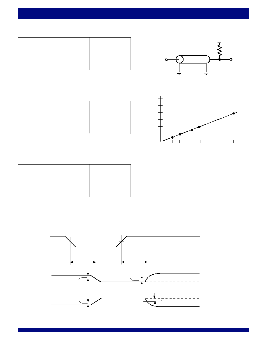
1.5V AC TEST CONDITIONS
Figure 2b. Lumped Capacitive Load, Typical Derating
AC TEST LOADS
Figure 2a. AC Test Load
Input Pulse Levels
0.4 to 1.4V
Input Rise/Fall Times
0.4ns
Input Timing Reference Levels
0.9
Output Reference Levels
V
DDQ
/2
EXTENDED HSTL
1.8V AC TEST CONDITIONS
Input Pulse Levels
GND to 2.5V
Input Rise/Fall Times
1ns
Input Timing Reference Levels
V
CC
/2
Output Reference Levels
V
DDQ
/2
2.5V LVTTL
2.5V AC TEST CONDITIONS
5998 drw04
50
V
DDQ
/2
I/O
Z
0
= 50
5998 drw04a
6
5
4
3
2
1
20 30 50
80 100
200
Capacitance (pF)
t
CD
(Typical, ns)
NOTE:
1. V
DDQ
= 1.5VĪ.
NOTE:
1. V
DDQ
= 1.8VĪ.
NOTE:
1. For LVTTL V
CC
= V
DDQ
.
OUTPUT ENABLE & DISABLE TIMING
V
IH
OE
V
IL
t
OE &
t
OLZ
100mV
100mV
t
OHZ
100mV
100mV
Output
Normally
LOW
Output
Normally
HIGH
V
OL
V
OH
V
CC
/2
5998 drw04b
Output
Enable
Output
Disable
V
CC
/2
V
CC
/2
V
CC
/2
NOTE:
1.
REN is HIGH.

17
IDT72T51546/72T51556 2.5V, MULTI-QUEUE FLOW-CONTROL DEVICES
(32 QUEUES) 36 BIT WIDE CONFIGURATION 1,179,648 and 2,359,296 bits
COMMERCIAL AND INDUSTRIAL
TEMPERATURE RANGES
P R E L I M I N A R
Y
AC ELECTRICAL CHARACTERISTICS
(Commercial: V
CC
= 2.5V Ī 0.15V, T
A
= 0
įC to +70įC;Industrial: V
CC
= 2.5V Ī 0.15V, T
A
= -40
įC to +85įC; JEDEC JESD8-A compliant)
Commercial
Com'l & Ind'l
(1)
IDT72T51546L5
IDT72T51546L6
IDT72T51556L5
IDT72T51556L6
Symbol
Parameter
Min.
Max.
Min.
Max.
Unit
f
S
Clock Cycle Frequency (WCLK & RCLK)
--
200
--
166
MHz
t
A
Data Access Time
0.6
3.6
0.6
3.7
ns
t
CLK
Clock Cycle Time
5
--
6
--
ns
t
CLKH
Clock High Time
2.3
--
2.7
--
ns
t
CLKL
Clock Low Time
2.3
--
2.7
--
ns
t
DS
Data Setup Time
1.5
--
2.0
--
ns
t
DH
Data Hold Time
0.5
--
0.5
--
ns
t
ENS
Enable Setup Time
1.5
--
2.0
--
ns
t
ENH
Enable Hold Time
0.5
--
0.5
--
ns
t
RS
Reset Pulse Width
30
--
30
--
ns
t
RSS
Reset Setup Time
15
--
15
--
ns
t
RSR
Reset Recovery Time
10
--
10
--
ns
t
PRSS
Partial Reset Setup
1.5
--
2.0
--
ns
t
PRSH
Partial Reset Hold
0.5
--
0.5
--
ns
t
OLZ (
OE-
Q
n)
(2)
Output Enable to Output in Low-Impedance
0.6
3.6
0.6
3.7
ns
t
OHZ
(2)
Output Enable to Output in High-Impedance
0.6
3.6
0.6
3.7
ns
t
OE
Output Enable to Data Output Valid
0.6
3.6
0.6
3.7
ns
f
C
Clock Cycle Frequency (SCLK)
--
10
--
10
MHz
t
SCLK
Serial Clock Cycle
100
--
100
--
ns
t
SCKH
Serial Clock High
45
--
45
--
ns
t
SCKL
Serial Clock Low
45
--
45
--
ns
t
SDS
Serial Data In Setup
20
--
20
--
ns
t
SDH
Serial Data In Hold
1.2
--
1.2
--
ns
t
SENS
Serial Enable Setup
20
--
20
--
ns
t
SENH
Serial Enable Hold
1.2
--
1.2
--
ns
t
SDO
SCLK to Serial Data Out
--
20
--
20
ns
t
SENO
SCLK to Serial Enable Out
--
20
--
20
ns
t
SDOP
Serial Data Out Propagation Delay
1.5
3.7
1.5
3.7
ns
t
SENOP
Serial Enable Propagation Delay
1.5
3.7
1.5
3.7
ns
t
PCWQ
Programming Complete to Write Queue Selection
20
--
20
--
ns
t
PCRQ
Programming Complete to Read Queue Selection
20
--
20
ns
t
AS
Address Setup
1.5
--
2.5
--
ns
t
AH
Address Hold
1.0
--
1.5
--
ns
t
WFF
Write Clock to Full Flag
--
3.6
--
3.7
ns
t
ROV
Read Clock to Output Valid
--
3.6
--
3.7
ns
t
STS
PAE/PAF Strobe Setup
1.5
--
2.0
--
ns
t
STH
PAE/PAF Strobe Hold
0.5
--
0.5
--
ns
t
QS
Queue Setup
1.5
--
2.0
--
ns
t
QH
Queue Hold
1.0
--
0.5
--
ns
t
WAF
WCLK to
PAF flag
0.6
3.6
0.6
3.7
ns
t
RAE
RCLK to
PAE flag
0.6
3.6
0.6
3.7
ns
t
PAF
Write Clock to Synchronous Almost-Full Flag Bus
0.6
3.6
0.6
3.7
ns
t
PAE
Read Clock to Synchronous Almost-Empty Flag Bus
0.6
3.6
0.6
3.7
ns
NOTES:
1. Industrial temperature range product for the 6ns is available as a standard device. All other speed grades available by special order.
2. Values guaranteed by design, not currently tested.

18
COMMERCIAL AND INDUSTRIAL
TEMPERATURE RANGES
IDT72T51546/72T51556 2.5V, MULTI-QUEUE FLOW-CONTROL DEVICES
(32 QUEUES) 36 BIT WIDE CONFIGURATION 1,179,648 and 2,359,296 bits
P R E L I M I N A R
Y
AC ELECTRICAL CHARACTERISTICS (CONTINUED)
(Commercial: V
CC
= 2.5V Ī 0.15V, T
A
= 0
įC to +70įC;Industrial: V
CC
= 2.5V Ī 0.15V, T
A
= -40
įC to +85įC; JEDEC JESD8-A compliant)
t
ERCLK
RCLK to Echo RCLK Output
--
4.0
--
4.2
ns
t
CLKEN
RCLK to Echo
REN Output
--
3.6
--
3.7
ns
t
PAELZ
(2)
RCLK to
PAE Flag Bus to Low-Impedance
0.6
3.6
0.6
3.7
ns
t
PAEHZ
(2)
RCLK to
PAE Flag Bus to High-Impedance
0.6
3.6
0.6
3.7
ns
t
PAFLZ
(2)
WCLK to
PAF Flag Bus to Low-Impedance
0.6
3.6
0.6
3.7
ns
t
PAFHZ
(2)
WCLK to
PAF Flag Bus to High-Impedance
0.6
3.6
0.6
3.7
ns
t
FFHZ
(2)
WCLK to Full Flag to High-Impedance
0.6
3.6
0.6
3.7
ns
t
FFLZ
(2)
WCLK to Full Flag to Low-Impedance
0.6
3.6
0.6
3.7
ns
t
OVLZ
(2)
RCLK to Output Valid Flag to Low-Impedance
0.6
3.6
0.6
3.7
ns
t
OVHZ
(2)
RCLK to Output Valid Flag to High-Impedance
0.6
3.6
0.6
3.7
ns
t
FSYNC
WCLK to
PAF Bus Sync to Output
0.6
3.6
0.6
3.7
ns
t
FXO
WCLK to
PAF Bus Expansion to Output
0.6
3.6
0.6
3.7
ns
t
ESYNC
RCLK to
PAE Bus Sync to Output
0.6
3.6
0.6
3.7
ns
t
EXO
RCLK to
PAE Bus Expansion to Output
0.6
3.6
0.6
3.7
ns
t
PR
RCLK to Packet Ready Flag
0.6
3.6
0.6
3.7
ns
t
SKEW1
SKEW
time between RCLK and WCLK for
FF and OV
4
--
4.5
--
ns
t
SKEW2
SKEW
time between RCLK and WCLK for
PAF and PAE
5
--
6
--
ns
t
SKEW3
SKEW
time between RCLK and WCLK for
PAF[0:7] and PAE[0:7]
5
--
6
--
ns
t
SKEW4
SKEW
time between RCLK and WCLK for
PR and OV
5
--
6
--
ns
t
SKEW5
SKEW
time between RCLK and WCLK for
OV when in Packet Mode
8
--
10
--
ns
t
XIS
Expansion Input Setup
1.0
--
1.0
--
ns
t
XIH
Expansion Input Hold
0.5
--
0.5
--
ns
Commercial
Com'l & Ind'l
(1)
IDT72T51546L5
IDT72T51546L6
IDT72T51556L5
IDT72T51556L6
Symbol
Parameter
Min.
Max.
Min.
Max.
Unit
NOTES:
1. Industrial temperature range product for the 6ns is available as a standard device. All other speed grades available by special order.
2. Values guaranteed by design, not currently tested.

19
IDT72T51546/72T51556 2.5V, MULTI-QUEUE FLOW-CONTROL DEVICES
(32 QUEUES) 36 BIT WIDE CONFIGURATION 1,179,648 and 2,359,296 bits
COMMERCIAL AND INDUSTRIAL
TEMPERATURE RANGES
FUNCTIONAL DESCRIPTION
MASTER RESET
A Master Reset is performed by toggling the
MRS input from HIGH to LOW
to HIGH. During a master reset all internal multi-queue device setup and control
registers are initialized and require programming either serially by the user via
the serial port, or using the default settings. During a master reset the state of
the following inputs determine the functionality of the part, these pins should be
held HIGH or LOW.
PKT ≠ Packet Mode
FM ≠ Flag bus Mode
IW, OW, BM ≠ Bus Matching options
MAST ≠ Master Device
ID0, 1, 2 ≠ Device ID
DFM ≠ Programming mode, serial or default
DF ≠ Offset value for
PAE and PAF
Once a master reset has taken place, the device must be programmed either
serially or via the default method before any read/write operations can begin.
See Figure 5, Master Reset for relevant timing.
PARTIAL RESET
A Partial Reset is a means by which the user can reset both the read and write
pointers of a single queue that has been setup within a multi-queue device.
Before a partial reset can take place on a queue, the respective queue must be
selected on both the read port and write port a minimum of 2 RCLK and 2 WCLK
cycles before the
PRS goes LOW. The partial reset is then performed by toggling
the
PRS input from HIGH to LOW to HIGH, maintaining the LOW state for at least
one WCLK and one RCLK cycle. Once a partial reset has taken place a minimum
of 3 WCLK and 3 RCLK cycles must occur before enabled writes or reads can
occur.
A Partial Reset only resets the read and write pointers of a given queue, a
partial reset will not effect the overall configuration and setup of the multi-queue
device and its queues.
See Figure 6, Partial Reset for relevant timing.
SERIAL PROGRAMMING
The multi-queue flow-control device is a fully programmable device, provid-
ing the user with flexibility in how queues are configured in terms of the number
of queues, depth of each queue and position of the
PAF/PAE flags within
respective queues. All user programming is done via the serial port after a master
reset has taken place. Internally the multi-queue device has setup registers
which must be serially loaded, these registers contain values for every queue
within the device, such as the depth and
PAE/PAF offset values. The
IDT72T51546/72T51556 devices are capable of up to 32 queues and
therefore contain 32 sets of registers for the setup of each queue.
During a Master Reset if the DFM (Default Mode) input is LOW, then the device
will require serial programming by the user. It is recommended that the user
utilize a `C' program provided by IDT, this program will prompt the user for all
information regarding the multi-queue setup. The program will then generate
a serial bit stream which should be serially loaded into the device via the serial
port. For the IDT72T51546/72T51556 devices the serial programming re-
quires a total number of serially loaded bits per device, (SCLK cycles with
SENI
enabled), calculated by: 19+(Qx72) where Q is the number of queues the user
wishes to setup within the device.
Once the master reset is complete and
MRS is HIGH, the device can be
serially loaded. Data present on the SI (serial in), input is loaded into the serial
port on a rising edge of SCLK (serial clock), provided that
SENI (serial in
enable), is LOW. Once serial programming of the device has been successfully
completed the device will indicate this via the
SENO (serial output enable) going
active, LOW. Upon detection of completion of programming, the user should
cease all programming and take
SENI inactive, HIGH. Note, SENO follows SENI
once programming of a device is complete. Therefore,
SENO will go LOW after
programming provided
SENI is LOW, once SENI is taken HIGH again, SENO
will also go HIGH. The operation of the SO output is similar, when programming
of a given device is complete, the SO output will follow the SI input.
If devices are being used in expansion mode the serial ports of devices should
be cascaded. The user can load all devices via the serial input port control pins,
SI &
SENI, of the first device in the chain. Again, the user may utilize the `C'
program to generate the serial bit stream, the program prompting the user for
the number of devices to be programmed. The
SENO and SO (serial out) of
the first device should be connected to the
SENI and SI inputs of the second
device respectively and so on, with the
SENO & SO outputs connecting to the
SENI & SI inputs of all devices through the chain. All devices in the chain should
be connected to a common SCLK. The serial output port of the final device should
be monitored by the user. When
SENO of the final device goes LOW, this
indicates that serial programming of all devices has been successfully com-
pleted. Upon detection of completion of programming, the user should cease all
programming and take
SENI of the first device in the chain inactive, HIGH.
As mentioned, the first device in the chain has its serial input port controlled
by the user, this is the first device to have its internal registers serially loaded
by the serial bit stream. When programming of this device is complete it will take
its
SENO output LOW and bypass the serial data loaded on the SI input to its
SO output. The serial input of the second device in the chain is now loaded with
the data from the SO of the first device, while the second device has its
SENI
input LOW. This process continues through the chain until all devices are
programmed and the
SENO of the final device goes LOW.
Once all serial programming has been successfully completed, normal
operations, (queue selections on the read and write ports) may begin. When
connected in expansion mode, the IDT72T51546/72T51556 devices require
a total number of serially loaded bits per device to complete serial programming,
(SCLK cycles with
SENI enabled), calculated by: n[19+(Qx72)] where Q is the
number of queues the user wishes to setup within the device, where n is the
number of devices in the chain.
See Figure 7, Serial Port Connection and Figure 8, Serial Programming for
connection and timing information.
DEFAULT PROGRAMMING
During a Master Reset if the DFM (Default Mode) input is HIGH the multi-
queue device will be configured for default programming, (serial programming
is not permitted). Default programming provides the user with a simpler,
however limited means by which to setup the multi-queue flow-control device,
rather than using the serial programming method. The default mode will
configure a multi-queue device such that the maximum number of queues
possible are setup, with all of the parts available memory blocks being allocated
equally between the queues. The values of the
PAE/PAF offsets is determined
by the state of the DF (default) pin during a master reset.
For the IDT72T51546/72T51556 devices the default mode will setup 32
queues, each queue being 1024 x36 and 2048 x36 deep respectively. For both
devices the value of the
PAE/PAF offsets is determined at master reset by the
state of the DF input. If DF is LOW then both the
PAE & PAF offset will be 8, if
HIGH then the value is 128.
When configuring the IDT72T51546/72T51556 devices in default mode the
user simply has to apply WCLK cycles after a master reset, until
SENO goes
LOW, this signals that default programming is complete. These clock cycles are
required for the device to load its internal setup registers. When a single multi-
queue device is used, the completion of device programming is signaled by the
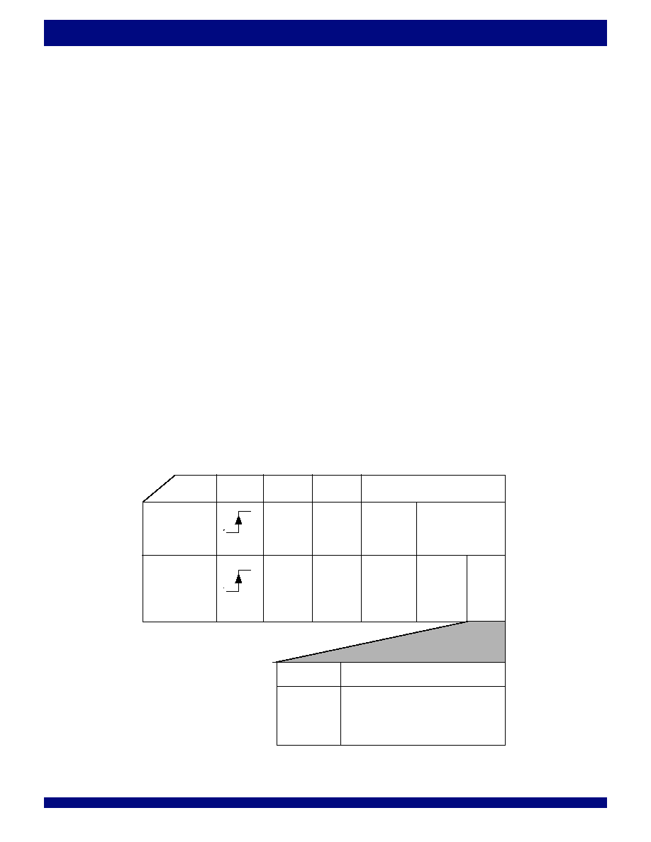
20
COMMERCIAL AND INDUSTRIAL
TEMPERATURE RANGES
IDT72T51546/72T51556 2.5V, MULTI-QUEUE FLOW-CONTROL DEVICES
(32 QUEUES) 36 BIT WIDE CONFIGURATION 1,179,648 and 2,359,296 bits
SENO output of a device going from HIGH to LOW. Note, that SENI must be
held LOW when a device is setup for default programming mode.
When multi-queue devices are connected in expansion mode, the
SENI of
the first device in a chain can be held LOW. The
SENO of a device should
connect to the
SENI of the next device in the chain. The SENO of the final device
is used to indicate that default programming of all devices is complete. When the
final
SENO goes LOW normal operations may begin. Again, all devices will be
programmed with their maximum number of queues and the memory divided
equally between them. Please refer to Figure 9, Default Programming.
READING AND WRITING TO THE IDT MULTI-QUEUE
FLOW-CONTROL DEVICE
The IDT72T51546/72T51556 multi-queue flow-control devices can be
configured in two distinct modes, namely Standard Mode and Packet Mode.
STANDARD MODE OPERATION (PKT = LOW ON MASTER RESET)
WRITE QUEUE SELECTION AND WRITE OPERATION
(STANDARD MODE)
The IDT72T51546/72T51556 multi-queue flow-control devices can be
configured up to a maximum of 32 queues into which data can be written via
a common write port using the data inputs (Din), write clock (WCLK) and write
enable (
WEN). The queue to be written is selected by the address present on
the write address bus (WRADD) during a rising edge on WCLK while write
address enable (WADEN) is HIGH. The state of
WEN does not impact the queue
selection. The queue selection requires 1 WCLK cycle. All subsequent data
writes will be to this queue until another queue is selected.
Standard mode operation is defined as individual words will be written to the
device as opposed to Packet Mode where complete packets may be written.
The write port is designed such that 100% bus utilization can be obtained. This
means that data can be written into the device on every WCLK rising edge
including the cycle that a new queue is being addressed.
Changing queues requires a minimum of 3 WCLK cycles on the write port
(see Figure 10, Write Queue Select, Write Operation and Full flag Operation).
WADEN goes high signaling a change of queue (clock cycle "A"). The address
on WRADD at that time determines the next queue. Data presented during that
cycle ("A") and the next cycle ("B" and "C"), will be written to the active (old)
queue, provided
WEN is active LOW. If WEN is HIGH (inactive) for these 3 clock
cycles, data will not be written in to the previous queue. The write port discrete
full flag will update to show the full status of the newly selected queue (Q
X
) at this
last cycle's rising edge ("C"). Data present on the data input bus (Din), can be
written into the newly selected queue (Q
X
) on the rising edge of WCLK on the
third cycle ("D") following a change of queue, provided
WEN is LOW and the
new queue is not full. If the newly selected queue is full at the point of its selection,
any writes to that queue will be prevented. Data cannot be written into a full
queue.
Refer to Figure 10, Write Queue Select, Write Operation and Full flag
Operation, Figure 11, Write Operations & First Word Fall Through for timing
diagrams and Figure 12, Full Flag Timing in Expansion Mode for timing
diagrams.
TABLE 1 -- WRITE ADDRESS BUS, WRADD[7:0]
Operation WCLK WADEN
FSTR
WRADD[7:0]
Write
Queue
Select
1
0
0
1
Device Select
(Compared to
ID0,1,2)
Write Queue Address
(5 bits = 32 Queues)
7
6
5
4 3 2
1 0
7
6
5
4 3 2
1 0
Device Select
(Compared to
ID0,1,2)
X
X
X
Quadrant
Address
PAFn
Quadrant
Select
Q0 : Q7
PAF0 : PAF7
Quadrant
Address
Queue Status on
PAFn Bus
00
01
10
11
Q8 : Q15
PAF0 : PAF7
Q16 : Q23
PAF0 : PAF7
Q24 : Q31
PAF0 : PAF7
5998 drw05
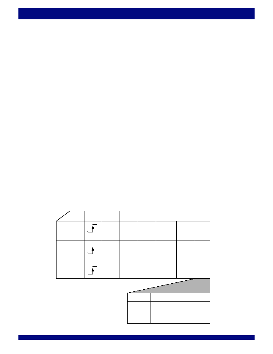
21
IDT72T51546/72T51556 2.5V, MULTI-QUEUE FLOW-CONTROL DEVICES
(32 QUEUES) 36 BIT WIDE CONFIGURATION 1,179,648 and 2,359,296 bits
COMMERCIAL AND INDUSTRIAL
TEMPERATURE RANGES
READ QUEUE SELECTION AND READ OPERATION
(STANDARD MODE)
The IDT72T51546/72T51556 multi-queue flow-control devices can be
configured up to a maximum of 32 queues which data can be read via a common
read port using the data outputs (Qout), read clock (RCLK) and read enable
(
REN). An output enable, OE control pin is also provided to allow High-
Impedance selection of the Qout data outputs. The multi-queue device read port
operates in a mode similar to "First Word Fall Through" on a SuperSync IDT
FIFO, but with the added feature of data output pipelining (see Figure 11, Write
Operations & First Word Fall Through). The queue to be read is selected by
the address presented on the read address bus (RDADD) during a rising edge
on RCLK while read address enable (RADEN) is HIGH. The state of
REN does
not impact the queue selection. The queue selection requires 1 RCLK cycles.
All subsequent data reads will be from this queue until another queue is selected.
Standard mode operation is defined as individual words will be read from the
device as opposed to Packet Mode where complete packets may be read. The
read port is designed such that 100% bus utilization can be obtained. This means
that data can be read out of the device on every RCLK rising edge including
the cycle that a new queue is being addressed.
Changing queues requires a minimum of three RCLK cycles on the read port
(see Figure 13, Read Queue Select, Read Operation). RADEN goes high
signaling a change of queue (clock cycle "D"). The address on RDADD at that
time determines the next queue. Data presented during that cycle ("D") will be
read at "D" (+ t
A
), and the next cycle ("E"), can continue to be read from the active
(old) queue (Q
P
), provided
REN is active LOW. If REN is HIGH (inactive) for
these two clock cycles, data will not be read from the previous queue. The next
cycle's rising edge ("F"), the read port discrete empty flag will update to show
the empty status of the newly selected queue (Q
F
). The internal pipeline is also
loaded at this time ("F") with the last word from the previous (old) queue (Q
F
)
as well as the next word from the new queue (Q
F
). Both of these words will fall
through to the output register (provided the
OE is asserted) consecutively
(cycles "F" and "G" respectively) following the selection of the new queue
regardless of the state of
REN, unless the new queue (Q
F
) is empty. If the newly
selected queue is empty, any reads from that queue will be prevented. Data
cannot be read from an empty queue. The last word in the data output register
(from the previous queue), will remain on the data bus, but the output valid flag,
OV will go HIGH, to indicate that the data present is no longer valid. This pipelining
effect provides the user with 100% bus utilization, and brings about the possibility
that a "NULL" queue may be required within a multi-queue device. Null queue
operation is discussed in the next section. Remember that
OE allows the user
to place the data output bus (Qout) into High-Impedance and the data can be
read in to the output register regardless of
OE.
Refer to Table 2, for Read Address Bus arrangement. Also, refer to Figures
13, 15, and 16 for read queue selection and read port operation timing diagrams.
PACKET MODE OPERATION (PKT = HIGH on Master Reset)
The Packet mode operation provides the capability where, user defined
packets or frames can be written to the device as opposed to Standard mode
where individual words are written. For clarification, in Packet Mode, a packet
can be written to the device with the starting location designated as Transmit Start
of Packet (TSOP) and the ending location designated as Transmit End of Packet
(TEOP). In conjunction, a packet read from the device will be designated as
Operation RCLK
RADEN
ESTR
RDADD[7:0]
Read Queue
Select
1
0
0
1
Device Select
(Compared to
ID0,1,2)
Read Queue Address
(5 bits = 32 Queues)
7
6
5
4 3 2
1 0
7
6
5
4 3 2
1 0
Device Select
(Compared to
ID0,1,2)
X
X
X
Quadrant
Address
PAEn/PRn
Quadrant
Select
Q0 : Q7
PAE0 : PAE7
Quadrant
Address
Queue Status on
PAEn/PRn Bus
00
01
10
11
Q8 : Q15
PAE0 : PAE7
Q16 : Q23
PAE0 : PAE7
Q24 : Q31
PAE0 : PAE7
5998 drw06
Null-Q
0
0
1
0
7
6
5
4 3 2
1 0
X
X
X
Null Queue
Select
1
X
X
X
X
X
TABLE 2 -- READ ADDRESS BUS, RDADD[7:0]

22
COMMERCIAL AND INDUSTRIAL
TEMPERATURE RANGES
IDT72T51546/72T51556 2.5V, MULTI-QUEUE FLOW-CONTROL DEVICES
(32 QUEUES) 36 BIT WIDE CONFIGURATION 1,179,648 and 2,359,296 bits
Receive Start of Packet (RSOP) and a Receive End of Packet (REOP). The
minimum size for a packet is four words (SOP, two words of data and EOP). The
almost empty flag bus becomes the "Packet Ready"
PR flag bus when the device
is configured for packet mode. Valid packets are indicated when both
PR and
OV are asserted.
WRITE QUEUE SELECTION AND WRITE OPERATION (PACKET MODE)
It is required that a full packet be written to a queue before moving to a different
queue. The device requires three cycles to change queues. Packet mode, has
2 restrictions: <1> An extra word (or filler word) is required to be written after
each packet on the cycle following the queue change to ensure the RSOP in
the old queue is not read out on a queue change because of the first word fall
through. <2> No SOP/EOP is allowed to read/written at cycle ("D" or "K") the
second cycle after a queue change. In this mode, the write port may not obtain
100% bus utilization.
Changing queues requires a minimum of 3 WCLK cycles on the write port
(see Figure 17, Writing in Packet Mode during a Queue Change). WADEN
goes high signaling a change of queue (clock cycle "B" or "I"). The address
on WRADD at the rising edge of WCLK determines the next queue. Data
presented on Din during that cycle ("B" or "I") and the next cycle ("C" or "J")
can continue to be written to the active (old) queue (Q
A
or Q
B
respectively),
provided
WEN is LOW (active). If WEN is HIGH (inactive) for these two clock
cycles (H), data will not be written in to the previous queue (Q
A
). The second
cycle following a request for queue change ("D" or "K") will require a "filler" word
to be written to the device. This can be done by clocking the TEOP twice or by
writing a "filler" word. In packet mode, the multi-queue is designed under the
2 restrictions listed previously. Note, an erroneous Packet Ready flag may occur
if the EOP or SOP marker shows up at the second cycle after a queue change.
To prevent an erroneous Packet Ready flag from occurring a filler word should
be written into the old queue at the last clock cycle of writing. It is important to know
that no SOP or EOP may be written into the device during this cycle ("D" or "K").
The write port discrete full flag will update to show the full status of the newly
selected queue (Q
B
) at this last cycle's rising edge ("D" or "K"). Data values
presented on the data input bus (Din), can be written into the newly selected
queue (Q
X
) on the rising edge of WCLK on the third cycle ("E") following a request
for change of queue, provided
WEN is LOW (active) and the new queue is not
full. If a selected queue is full (
FF is LOW), then writes to that queue will be
prevented. Note, data cannot be written into a full queue.
Refer to Figure 17, Writing in Packet Mode during a Queue Change and
Figure 19, Data Input (Transit) Packet Mode of Operation for timing diagrams.
READ QUEUE SELECTION AND READ OPERATION (PACKET MODE)
In packet Mode it is required that a full packet is read from a queue before
moving to a different queue. The device requires three cycles to change queues.
In Packet Mode, there are 2 restrictions <1> An extra word (or filler word) should
have been inserted into the data stream after each packet to insure the RSOP
in the old queue is not read out on a queue change because of the first word
fall through and this word should be discarded. <2> No EOP/SOP is allowed
to be read/written at cycle ("D" or "K") the second cycle after a queue change).
In this mode, the read port may not obtain 100% bus utilization.
Changing queues requires a minimum of 3 RCLK cycles on the read port (see
Figure 18, Reading in Packet Mode during a Queue Change). RADEN goes
high signaling a change of queue (clock cycle "B" or "I"). The address on
RDADD at the rising edge of RCLK determines the queue. As illustrated in Figure
18 during cycle ("B" or "I"), and the next cycle ("C" or "J") data can continue
to be read from the active (old) queue (Q
A
or Q
B
respectively), provided both
REN and OE are LOW (active) simultaneously with changing queues. REOP
for packet located in queue (Q
A
) must be read on or before a queue change
request is made ("C" or "J"). If
REN is HIGH (inactive) for these two clock cycles,
data will not be read from the previous queue (Q
A
). In applications where the
multi-queue flow-control device is connected to a shared bus, an output enable,
OE control pin is also provided to allow High-Impedance selection of the data
outputs (Qout). With reference to Figure 18 when changing queues, a packet
marker (SOP or EOP) should not be read on cycle ("E" or "L"). Reading a SOP
or EOP should not occur during the cycles required for a queue change. It is
also recommended that a queue change should not occur once the reading of
the packet has commenced, The EOP marker of the packet prior to a queue
change should be read on or before the queue change. If the EOP word is read
before a queue change,
REN can be pulled high to disable further reads. When
the queue change is initiated, the filler word written into the current queue after
the EOP word will fall through followed by and the first word from the new queue.
Refer to Figure 18, Reading in Packet Mode during a Queue Change as
well as Figures 13, 15, and 16 for timing diagrams and Table 2, for Read Address
bus arrangement.
Note, the almost empty flag bus becomes the "Packet Ready" flag bus when
the device is configured for packet ready mode. .
PACKET READY FLAG
The 36-bit multi-queue flow-control device provides the user with a Packet
Ready feature. During a Master Reset the logic "1" (HIGH) on the PKT input
signal (packet mode select), configures the device in packet mode. The
PR
discrete flag, provides a packet ready status of the active queue selected on the
read port. A packet ready status is individually maintained on all queues;
however only the queue selected on the read port has its packet ready status
indicated on the
PR output flag. A packet is available on the output for reading
when both
PR and OV are asserted LOW. If less than a full packet is available,
the
PR flag will be HIGH (packet not ready). In packet mode, no words can be
read from a queue until a complete packet has been written into that queue,
regardless of
REN.
When packet mode is selected the Programmable Almost Empty bus,
PAEn,
becomes the Packet Ready bus,
PRn. When configured in Direct Bus (FM =
LOW during a master reset), the
PRn bus provides packet ready status in 8
queue increments. The
PRn bus supports either Polled or Direct modes of
operation. The
PRn mode of operation is configured through the Flag Mode
(FM) bit during a Master Reset.
When the multi-queue is configured for packet mode operation, the device
must also be configured for 36 bit write data bus and 36 bit read data bus. The
two most significant bits of the 36-bit data bus are used as "packet markers". On
the write port these are bits D34 (Transmit Start of Packet,) D35 (Transmit End
of Packet) and on the read port Q34, Q35. All four bits are monitored by the packet
control logic as data is written into and read out from the queues. The packet
ready status for individual queues is then determined by the packet ready logic.
On the write port D34 is used to "mark" the first word being written into the
selected queue as the "Transmit Start of Packet", TSOP. To further clarify, when
the user requires a word being written to be marked as the start of a packet, the
TSOP input (D34) must be HIGH for the same WCLK rising edge as the word
that is written. The TSOP marker is stored in the queue along with the data it was
written in until the word is read out of the queue via the read port.
On the write port D35 is used to "mark" the last word of the packet currently
being written into the selected queue as the "Transmit End of Packet" TEOP.
When the user requires a word being written to be marked as the end of a packet,
the TEOP input must be HIGH for the same WCLK rising edge as the word that
is written in. The TEOP marker is stored in the queue along with the data it was
written in until the word is read out of the queue via the read port.
The packet ready logic monitors all start and end of packet markers both as
they enter respective queues via the write port and as they exit queues via the
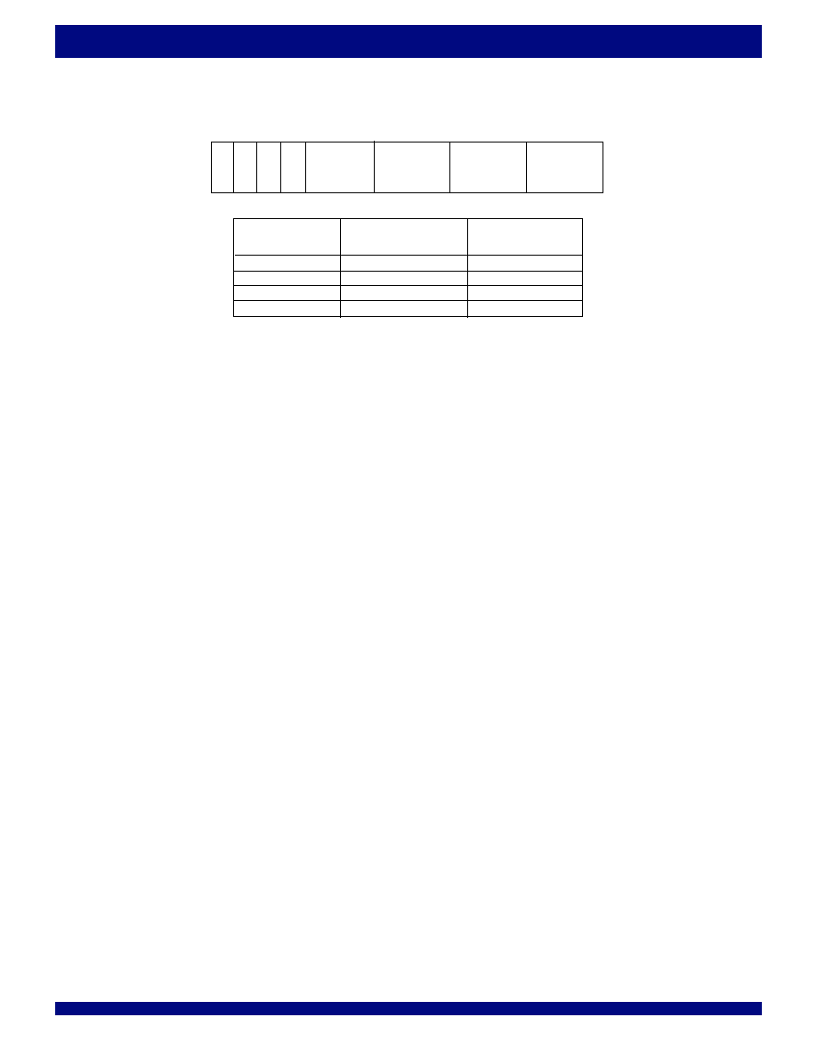
23
IDT72T51546/72T51556 2.5V, MULTI-QUEUE FLOW-CONTROL DEVICES
(32 QUEUES) 36 BIT WIDE CONFIGURATION 1,179,648 and 2,359,296 bits
COMMERCIAL AND INDUSTRIAL
TEMPERATURE RANGES
read port. The multi-queue internal logic increments and decrements a packet
counter, which is provided for each queue. The functionality of the packet ready
logic provides status as to whether at least one full packet of data is available
within the selected queue. A partial packet in a queue is regarded as a packet
not ready and
PR (active LOW) will be HIGH. In Packet mode, no words can
be read from a queue until at least one complete packet has been written into
the queue, regardless of
REN. For example, if a TSOP has been written and
some number of words later a TEOP is written a full packet of data is deemed
to be available, and the
PR flag and OV will go active LOW. Consequently if reads
begin from a queue that has only one complete packet and the RSOP is detected
on the output port as data is being read out,
PR will go inactive HIGH. OV will
remain LOW indicating there is still valid data being read out of that queue until
the REOP is read. The user may proceed with the reading operation until the
current packet has been read out and no further complete packets are available.
If during that time another complete packet has been written into the queue and
the
PR flag will again gone active, then reads from the new packet may follow
after the current packet has been completely read out.
The packet counters therefore look for start of packet markers followed by end
of packet markers and regard data in between the TSOP and TEOP as a full
packet of data. The packet monitoring has no limitation as to how many packets
are written into a queue, the only constraint is the depth of the queue. Note, there
is a minimum allowable packet size of four words, inclusive of the TSOP marker
and TEOP marker.
The packet logic does expect a TSOP marker to be followed by a TEOP
marker.
If a second TSOP marker is written after a first, it is ignored and the logic
regards data between the first TSOP and the first subsequent TEOP as the full
packet. The same is true for TEOP; a second consecutive TEOP mark is ignored.
On the read side the user should regard a packet as being between the first
RSOP and the first subsequent REOP and disregard consecutive RSOP
markers and/or REOP markers. This is why a TEOP may be written twice, using
the second TEOP as the "filler" word.
As an example, the user may also wish to implement the use of an "Almost
End of Packet" (AEOP) marker. For example, the AEOP can be assigned to
data input bit D33. The purpose of this AEOP marker is to provide an indicator
that the end of packet is a fixed (known) number of reads away from the end
of packet. This is a useful feature when due to latencies within the system,
monitoring the REOP marker alone does not prevent "over reading" of the data
from the queue selected. For example, an AEOP marker set 4 writes before the
TEOP marker provides the device connected to the read port with and "almost
end of packet" indication 4 cycles before the end of packet.
The AEOP can be set any number of words before the end of packet
determined by user requirements or latencies involved in the system.
See Figure 18, Reading in Packet Mode during a Queue Change, Figure
19, Data Input (Transmit) Packet Mode of Operation and Figure 20, Data
Output (Receive) Packet Mode of Operation.
PACKET MODE ≠ MODULO OPERATION
The internal packet ready control logic performs no operation on these
modulo bits, they are only informational bits that are passed through with the
respective data byte(s).
When utilizing the multi-queue flow-control device in packet mode, the user
may also want to consider the implementation of "Modulo" operation or "valid
byte marking". Modulo operation may be useful when the packets being
transferred through a queue are in a specific byte arrangement even though
the data bus width is 36 bits. In Modulo operation the user can concatenate bytes
to form a specific data string through the multi-queue device. A possible scenario
is where a limited number of bytes are extracted from the packet for either
analysis or filtered for security protection. This will only occur when the first 36
bit word of a packet is written in and the last 36 bit word of packet is written in.
The modulo operation is a means by which the user can mark and identify specific
data within the Queue.
On the write port data input bits, D32 (transmit modulo bit 2, TMOD2) and D33
(transmit modulo bit 1, TMOD1) can be used as data markers. An example of
this could be to use D32 and D33 to code which bytes of a word are part of the
packet that is also being marked as the "Start of Marker" or "End of Marker".
Conversely on the read port when reading out these marked words, data
outputs Q32 (receive modulo bit 2, RMOD2) and Q33 (receive modulo bit 1,
RMOD1) will pass on the byte validity information for that word. Refer to Table
5 for one example of how the modulo bits may be setup and used. See Figure
19, Data Input (Transmit) Packet Mode of Operation and Figure 20, Data
Output (Receive) Packet Mode of Operation.
BYTE A
BYTE B
BYTE C
BYTE D
D0/Q0
D35/Q35
TMOD1 (D33)
RMOD1 (Q33)
TMOD2 (D32)
RMOD2 (Q32)
VALID BYTES
0
0
A, B, C, D
0
1
A
1
0
A, B
1
1
A, B, C
D15/Q15
D23/Q23
D31/Q31
D34/Q34
D33/Q33
D32/Q32
MOD 2
MOD 1
SOP
EOP
D7/Q7
5998 drw07
NOTE:
Packet Mode is only available when the Input Port and Output Port are 36 bits wide.
TABLE 5 -- PACKET MODE VALID BYTE

24
COMMERCIAL AND INDUSTRIAL
TEMPERATURE RANGES
IDT72T51546/72T51556 2.5V, MULTI-QUEUE FLOW-CONTROL DEVICES
(32 QUEUES) 36 BIT WIDE CONFIGURATION 1,179,648 and 2,359,296 bits
NULL QUEUE OPERATION (OF THE READ PORT)
Pipelining of data to the output port enables the device to provide 100% bus
utilization in standard mode. Data can be read out of the multi-queue flow-control
device on every RCLK cycle regardless of queue switches or other operations.
The device architecture is such that the pipeline is constantly filled with the next
words in a selected queue to be read out, again providing 100% bus utilization.
This type of architecture does assume that the user is constantly switching
queues such that during a queue switch, the last data word required from the
previous queue will fall through the pipeline to the output.
Note, that if reads cease at the empty boundary of a queue, then the last word
will automatically flow through the pipeline to the output.
The Null Q operation is achieved by setting the Null Q signal HIGH during
a queue select. Note that the read address bus RDADD[7:0] is a don't care. The
Null Queue is a separate queue within the device and thus the maximum number
of queues and memory is always available regardless of whether or not the Null
queue is used. Also note that in expansion mode a user may want to use a
dedicated null queue for each device. A null queue can be selected when no
further reads are required from a previously selected queue. Changing to a null
queue will continue to propagate data in the pipeline to the previous queue's
output. The Null Q can remain selected until a data becomes available in another
queue for reading. The Null-Q can be utilized in either standard or packet mode.
Note: If the user switches the read port to the null queue, this queue is seen
as and treated as an empty queue, therefore after switching to the null queue
the last word from the previous queue will remain in the output register and the
OV flag will go HIGH, indicating data is not valid.
The Null queue operation only has significance to the read port of the multi-
queue, it is a means to force data through the pipeline to the output. Null Q
selection and operation has no meaning on the write port of the device. Also,
refer to Figure 21, Read Operation and Null Queue Select for diagram.
PAFn FLAG BUS OPERATION
The IDT72T51546/72T51556 multi-queue flow-control device can be
configured for up to 32 queues, each queue having its own almost full status.
An active queue has its flag status output to the discrete flags,
FF and PAF, on
the write port. Queues that are not selected for a write operation can have their
PAF status monitored via the PAFn bus. The PAFn flag bus is 8 bits wide, so
that 8 queues at a time can have their status output to the bus. If 9 or more queues
are setup within a device then there are 2 methods by which the device can share
the bus between queues, "Direct" mode and "Polled" mode depending on the
state of the FM (Flag Mode) input during a Master Reset. If 8 or less queues
are setup within a device then each will have its own dedicated output from the
bus. If 8 or less queues are setup in single device mode, it is recommended to
configure the
PAFn bus to polled mode as it does not require using the write
address (WRADD).
EXPANDING UP TO 256 QUEUES OR PROVIDING DEEPER QUEUES
Expansion can take place using either the standard mode or the packet mode.
In the 32 queue multi-queue device, the WRADD address bus is 8 bits wide.
The 5 Least Significant bits (LSbs) are used to address one of the 32 available
queues within a single multi-queue device. The 3 Most Significant bits (MSbs)
are used when a device is connected in expansion mode with up to 8 devices
connected in width expansion, each device having its own 3-bit address. When
logically expanded with multiple parts, each device is statically setup with a
unique chip ID code on the ID pins, ID0, ID1, and ID2. A device is selected when
the 3 Most Significant bits of the WRADD address bus matches a 3-bit ID code.
The maximum logical expansion is 256 queues (32 queues x 8 devices) or a
minimum of 8 queues (1 queue per device x 8 devices), each of the maximum
size of the individual memory device.
Note: The WRADD bus is also used in conjunction with FSTR (almost full flag
bus strobe), to address the almost full flag bus during direct mode of operation.
Refer to Table 1, for Write Address bus arrangement. Also, refer to Figure
12, Full Flag Timing Expansion Mode, Figure 14, Output Valid Flag Timing (In
Expansion Mode), and Figure 35, Multi-Queue Expansion Diagram, for timing
diagrams.
BUS MATCHING OPERATION
Bus Matching operation between the input port and output port is available.
During a master reset of the multi-queue the state of the three setup pins, BM
(Bus Matching), IW (Input Width) and OW (Output Width) determine the input and
output port bus widths as per the selections shown in Table 3, "Bus Matching
Set-Up". 9 bit bytes, 18 bit words and 36 bit long words can be written into and
read from the Queues provided that at least one of the ports is setup for x36
operation. When writing to or reading from the multi-queue in a bus matching
mode, the device orders data in a "Little Endian" format. See Figure 4, Bus
Matching Byte Arrangement for details.
The Full flag and Almost Full flag operation is always based on writes and
reads of data widths determined by the write port width. For example, if the input
port is x36 and the output port is x9, then four data reads from a full queue will
be required to cause the full flag to go HIGH (queue not full). Conversely, the
Output Valid flag and Almost Empty flag operations are always based on writes
and reads of data widths determined by the read port. For example, if the input
port is x18 and the output port is x36, two write operations will be required to
cause the output valid flag of an empty queue to go LOW, output valid (queue
is not empty).
Note, that the input port serves all queues within a device, as does the output
port, therefore the input bus width to all queues is equal (determined by the input
port size) and the output bus width from all queues is equal (determined by the
output port size).
BM
I W
OW
Write Port
Read Port
0
X
X
x36
x36
1
0
0
x36
x18
1
0
1
x36
x9
1
1
0
x18
x36
1
1
1
x9
x36
x36 DEVICE
TABLE 3 -- BUS-MATCHING SET-UP
FULL FLAG OPERATION
The multi-queue flow-control device provides a single Full Flag output,
FF.
The
FF flag output provides a full status of the queue currently selected on the
write port for write operations. Internally the multi-queue flow-control device
monitors and maintains a status of the full condition of all queues within it, however
only the queue that is selected for write operations has its full status output to the
FF flag. This dedicated flag is often referred to as the "active queue full flag".
When queue switches are being made on the write port, the
FF flag output
will switch to the new queue and provide the user with the new queue status,
on the cycle after a new queue selection is made. The user then has a full status
for the new queue one cycle ahead of the WCLK rising edge that data can be
written into the new queue. That is, a new queue can be selected on the write
port via the WRADD bus, WADEN enable and a rising edge of WCLK. On the
second rising edge of WCLK, the
FF flag output will show the full status of the
newly selected queue. On the third rising edge of WCLK following the queue
selection, data can be written into the newly selected queue provided that data
and enable setup & hold times are met.

25
IDT72T51546/72T51556 2.5V, MULTI-QUEUE FLOW-CONTROL DEVICES
(32 QUEUES) 36 BIT WIDE CONFIGURATION 1,179,648 and 2,359,296 bits
COMMERCIAL AND INDUSTRIAL
TEMPERATURE RANGES
Note, the
FF flag will provide status of a newly selected queue two WCLK cycle
after queue selection, which is one cycle before data can be written to that queue.
This prevents the user from writing data to a queue that is full, (assuming that
a queue switch has been made to a queue that is actually full).
The
FF flag is synchronous to the WCLK and all transitions of the FF flag occur
based on a rising edge of WCLK. Internally the multi-queue device monitors and
keeps a record of the full status for all queues. It is possible that the status of a
FF flag maybe changing internally even though that flag is not the active queue
flag (selected on the write port). A queue selected on the read port may
experience a change of its internal full flag status based on read operations.
See Figure 10, Write Queue Select, Write Operation and Full Flag
Operation and Figure 12, Full Flag Timing in Expansion Mode for timing
information.
EXPANSION MODE - FULL FLAG OPERATION
When multi-queue devices are connected in Expansion mode the
FF flags
of all devices should be connected together, such that a system controller
monitoring and managing the multi-queue devices write port only looks at a
single
FF flag (as opposed to a discrete FF flag for each device). This FF flag
is only pertinent to the queue being selected for write operations at that time.
Remember, that when in expansion mode only one multi-queue device can be
written to at any moment in time, thus the
FF flag provides status of the active
queue on the write port.
This connection of flag outputs to create a single flag requires that the
FF flag
output have a High-Impedance capability, such that when a queue selection is
made only a single device drives the
FF flag bus and all other FF flag outputs
connected to the
FF flag bus are placed into High-Impedance. The user does
not have to select this High-Impedance state, a given multi-queue flow-control
device will automatically place its
FF flag output into High-Impedance when none
of its queues are selected for write operations.
When queues within a single device are selected for write operations, the
FF
flag output of that device will maintain control of the
FF flag bus. Its FF flag will
simply update between queue switches to show the respective queue full
status.
The multi-queue device places its
FF flag output into High-Impedance based
on the 3 bit ID code found in the 3 most significant bits of the write queue address
bus, WRADD. If the 3 most significant bits of WRADD match the 3 bit ID code setup
on the static inputs, ID0, ID1 and ID2 then the
FF flag output of the respective
device will be in a Low-Impedance state. If they do not match, then the
FF flag
output of the respective device will be in a High-Impedance state. See Figure
12, Full Flag Timing in Expansion Mode for details of flag operation, including
when more than one device is connected in expansion.
OUTPUT VALID FLAG OPERATION
The multi-queue flow-control device provides a single Output Valid flag
output,
OV. The OV provides an empty status or data output valid status for the
data word currently available on the output register of the read port. The rising
edge of an RCLK cycle that places new data onto the output register of the read
port, also updates the
OV flag to show whether or not that new data word is
actually valid. Internally the multi-queue flow-control device monitors and
maintains a status of the empty condition of all queues within it, however only
the queue that is selected for read operations has its output valid (empty) status
output to the
OV flag, giving a valid status for the word being read at that time.
The nature of the first word fall through operation means that when the last
data word is read from a selected queue, the
OV flag will go HIGH on the next
enabled read, that is, on the next rising edge of RCLK while
REN is LOW.
When queue switches are being made on the read port, the
OV flag will switch
to show status of the new queue in line with the data output from the new queue.
When a queue selection is made the first data from that queue will appear on
the Qout data outputs 3 RCLK cycles later, the
OV will change state to indicate
validity of the data from the newly selected queue on this 3
rd
RCLK cycle also.
The previous cycles will continue to output data from the previous queue and
the
OV flag will indicate the status of those outputs. Again, the OV flag always
indicates status for the data currently present on the output register.
The
OV flag is synchronous to the RCLK and all transitions of the OV flag occur
based on a rising edge of RCLK. Internally the multi-queue device monitors and
keeps a record of the output valid (empty) status for all queues. It is possible that
the status of an
OV flag may be changing internally even though that respective
flag is not the active queue flag (selected on the read port). A queue selected
on the write port may experience a change of its internal
OV flag status based
on write operations, that is, data may be written into that queue causing it to
become "not empty".
See Figure 13, Read Queue Select, Read Operation and Figure 14, Output
Valid Flag Timing for details of the timing.
EXPANSION MODE ≠ OUTPUT VALID FLAG OPERATION
When multi-queue devices are connected in Expansion mode, the
OV flags
of all devices should be connected together, such that a system controller
monitoring and managing the multi-queue devices read port only looks at a
single
OV flag (as opposed to a discrete OV flag for each device). This OV flag
is only pertinent to the queue being selected for read operations at that time.
Remember, that when in expansion mode only one multi-queue device can be
read from at any moment in time, thus the
OV flag provides status of the active
queue on the read port.
This connection of flag outputs to create a single flag requires that the
OV flag
output have a High-Impedance capability, such that when a queue selection is
made only a single device drives the
OV flag bus and all other OV flag outputs
connected to the
OV flag bus are placed into High-Impedance. The user does
not have to select this High-Impedance state, a given multi-queue flow-control
device will automatically place its
OV flag output into High-Impedance when none
of its queues are selected for read operations.
When queues within a single device are selected for read operations, the
OV
flag output of that device will maintain control of the
OV flag bus. Its OV flag will
simply update between queue switches to show the respective queue output
valid status.
The multi-queue device places its
OV flag output into High-Impedance based
on the 3 bit ID code found in the 3 most significant bits of the read queue address
bus, RDADD. If the 3 most significant bits of RDADD match the 3 bit ID code setup
on the static inputs, ID0, ID1 and ID2 then the
OV flag output of the respective
device will be in a Low-Impedance state. If they do not match, then the
OV flag
output of the respective device will be in a High-Impedance state. See Figure
14, Output Valid Flag Timing for details of flag operation, including when more
than one device is connected in expansion.
ALMOST FULL FLAG
As previously mentioned the multi-queue flow-control device provides a
single Programmable Almost Full flag output,
PAF. The PAF flag output provides
a status of the almost full condition for the active queue currently selected on the
write port for write operations. Internally the multi-queue flow-control device
monitors and maintains a status of the almost full condition of all queues within
it, however only the queue that is selected for write operations has its full status
output to the
PAF flag. This dedicated flag is often referred to as the "active queue
almost full flag". The position of the
PAF flag boundary within a queue can be
at any point within that queues depth. This location can be user programmed
via the serial port or one of the default values (8 or 128) can be selected if the
user has performed default programming.

26
COMMERCIAL AND INDUSTRIAL
TEMPERATURE RANGES
IDT72T51546/72T51556 2.5V, MULTI-QUEUE FLOW-CONTROL DEVICES
(32 QUEUES) 36 BIT WIDE CONFIGURATION 1,179,648 and 2,359,296 bits
As mentioned, every queue within a multi-queue device has its own almost
full status, when a queue is selected on the write port, this status is output via the
PAF flag. The PAF flag value for each queue is programmed during multi-queue
device programming (along with the number of queues, queue depths and
almost empty values). The
PAF offset value, m, for a respective queue can be
programmed to be anywhere between `0' and `D', where `D' is the total memory
depth for that queue. The
PAF value of different queues within the same device
can be different values.
When queue switches are being made on the write port, the
PAF flag output
will switch to the new queue and provide the user with the new queue status,
on the third cycle after a new queue selection is made, on the same WCLK cycle
that data can actually be written to the new queue. That is, a new queue can
be selected on the write port via the WRADD bus, WADEN enable and a rising
edge of WCLK. On the third rising edge of WCLK following a queue selection,
the
PAF flag output will show the full status of the newly selected queue. The PAF
is flag output is triple register buffered, so when a write operation occurs at the
almost full boundary causing the selected queue status to go almost full the
PAF
will go LOW 3 WCLK cycles after the write. The same is true when a read occurs,
there will be a 3 WCLK cycle delay after the read operation.
So the
PAF flag delays are:
from a write operation to
PAF flag LOW is 2 WCLK + t
WAF
The delay from a read operation to
PAF flag HIGH is t
SKEW2
+ WCLK + t
WAF
Note, if t
SKEW
is violated there will be one added WCLK cycle delay.
The
PAF flag is synchronous to the WCLK and all transitions of the PAF flag
occur based on a rising edge of WCLK. Internally the multi-queue device
monitors and keeps a record of the almost full status for all queues. It is possible
that the status of a
PAF flag maybe changing internally even though that flag is
not the active queue flag (selected on the write port). A queue selected on the
read port may experience a change of its internal almost full flag status based
on read operations. The multi-queue flow-control device also provides a
duplicate of the
PAF flag on the PAF[7:0] flag bus, this will be discussed in detail
in a later section of the data sheet.
See Figures 23 and 24 for Almost Full flag timing and queue switching.
ALMOST EMPTY FLAG
As previously mentioned the multi-queue flow-control device provides a
single Programmable Almost Empty flag output,
PAE. The PAE flag output
provides a status of the almost empty condition for the active queue currently
selected on the read port for read operations. Internally the multi-queue flow-
control device monitors and maintains a status of the almost empty condition of
all queues within it, however only the queue that is selected for read operations
has its empty status output to the
PAE flag. This dedicated flag is often referred
to as the "active queue almost empty flag". The position of the
PAE flag boundary
within a queue can be at any point within that queues depth. This location can
be user programmed via the serial port or one of the default values (8 or 128)
can be selected if the user has performed default programming.
As mentioned, every queue within a multi-queue device has its own almost
empty status, when a queue is selected on the read port, this status is output via
the
PAE flag. The PAE flag value for each queue is programmed during multi-
queue device programming (along with the number of queues, queue depths
and almost full values). The
PAE offset value, n, for a respective queue can be
programmed to be anywhere between `0' and `D', where `D' is the total memory
depth for that queue. The
PAE value of different queues within the same device
can be different values.
When queue switches are being made on the read port, the
PAE flag output
will switch to the new queue and provide the user with the new queue status,
on the third cycle after a new queue selection is made, on the same RCLK cycle
that data actually falls through to the output register from the new queue. That
is, a new queue can be selected on the read port via the RDADD bus, RADEN
enable and a rising edge of RCLK. On the third rising edge of RCLK following
a queue selection, the data word from the new queue will be available at the
output register and the
PAE flag output will show the empty status of the newly
selected queue. The
PAE is flag output is triple register buffered, so when a read
operation occurs at the almost empty boundary causing the selected queue
status to go almost empty the
PAE will go LOW 3 RCLK cycles after the read.
The same is true when a write occurs, there will be a 3 RCLK cycle delay after
the write operation.
So the
PAE flag delays are:
from a read operation to
PAE flag LOW is 2 RCLK + t
RAE
The delay from a write operation to
PAE flag HIGH is t
SKEW2
+ RCLK + t
RAE
Note, if t
SKEW
is violated there will be one added RCLK cycle delay.
The
PAE flag is synchronous to the RCLK and all transitions of the PAE flag
occur based on a rising edge of RCLK. Internally the multi-queue device
monitors and keeps a record of the almost empty status for all queues. It is possible
that the status of a
PAE flag maybe changing internally even though that flag is
not the active queue flag (selected on the read port). A queue selected on the
write port may experience a change of its internal almost empty flag status based
on write operations. The multi-queue flow-control device also provides a
duplicate of the
PAE flag on the PAE[7:0] flag bus, this will be discussed in detail
in a later section of the data sheet.
See Figures 25 and 26 for Almost Empty flag timing and queue switching.
POWER DOWN (PD)
This device has a power down feature intended for reducing power
consumption for HSTL/eHSTL configured inputs when the device is idle for a
long period of time. By entering the power down state certain inputs can be
disabled, thereby significantly reducing the power consumption of the part. All
WEN and REN signals must be disabled for a minimum of four WCLK and RCLK
cycles before activating the power down signal. The power down signal is
asynchronous and needs to be held LOW throughout the desired power down time.
During power down, the following conditions for the inputs/outputs signals are:
∑
All data in Queue(s) memory are retained.
∑
All data inputs become inactive.
∑
All write and read pointers maintain their last value before power down.
∑
All enables, chip selects, and clock input pins become inactive.
∑
All data outputs become inactive and enter high-impedance state.
∑
All flag outputs will maintain their current states before power down.
∑
All programmable flag offsets maintain their values.
∑
All echo clocks and enables will become inactive and enter high-
impedance state.
∑
The serial programming and JTAG port will become inactive and enter
high-impedance state.
∑
All setup and configuration CMOS static inputs are not affected, as these
pins are tied to a known value and do not toggle during operation.
All internal counters, registers, and flags will remain unchanged and maintain
their current state prior to power down. Clock inputs can be continuous and free-
running during power down, but will have no affect on the part. However, it is
recommended that the clock inputs be low when the power down is active. To
exit power down state and resume normal operations, disable the power down
signal by bringing it HIGH. There must be a minimum of 1
Ķs waiting period before
read and write operations can resume. The device will continue from where it
had stopped and no form of reset is required after exiting power down state. The
power down feature does not provide any power savings when the inputs are
configured for LVTTL operation. However, it will reduce the current for I/Os that
are not tied directly to V
CC
or GND. See Figure 34, Power Down Operation,
for the associated timing diagram.

27
IDT72T51546/72T51556 2.5V, MULTI-QUEUE FLOW-CONTROL DEVICES
(32 QUEUES) 36 BIT WIDE CONFIGURATION 1,179,648 and 2,359,296 bits
COMMERCIAL AND INDUSTRIAL
TEMPERATURE RANGES
TABLE 4 -- FLAG OPERATION BOUNDARIES & TIMING
Output Valid,
OV Flag Boundary
I/O Set-Up
OV Boundary Condition
In36 to out36 (Almost Empty Mode)
OV Goes LOW after 1
st
Write
(Both ports selected for same queue
(see note 1 below for timing)
when the 1
st
Word is written in)
In36 to out36 (Packet Mode)
OV Goes LOW after 1
st
Write
(Both ports selected for same queue
(see note 2 below for timing)
when the 1
st
Word is written in)
In36 to out18
OV Goes LOW after 1
st
Write
(Both ports selected for same queue
(see note 1 below for timing)
when the 1
st
Word is written in)
In36 to out9
OV Goes LOW after 1
st
Write
(Both ports selected for same queue
(see note 1 below for timing)
when the 1
st
Word is written in)
In18 to out36
OV Goes LOW after 1
st
Write
(Both ports selected for same queue
(see note 1 below for timing)
when the 1
st
Word is written in)
In9 to out36
OV Goes LOW after 1
st
Write
(Both ports selected for same queue
(see note 1 below for timing)
when the 1
st
Word is written in)
NOTE:
1.
OV Timing
Assertion:
Write to
OV LOW: t
SKEW1
+ RCLK + t
ROV
If t
SKEW1
is violated there may be 1 added clock: t
SKEW1
+ 2 RCLK + t
ROV
De-assertion:
Read Operation to
OV HIGH: t
ROV
2.
OV Timing when in Packet Mode (36 in to 36 out only)
Assertion:
Write to
OV LOW: t
SKEW4
+ RCLK + t
ROV
If t
SKEW4
is violated there may be 1 added clock: t
SKEW4
+ 2 RCLK + t
ROV
De-assertion:
Read Operation to
OV HIGH: t
ROV
NOTE:
D = Queue Depth
FF Timing
Assertion:
Write Operation to
FF LOW: t
WFF
De-assertion:
Read to
FF HIGH: t
SKEW1
+ t
WFF
If t
SKEW1
is violated there may be 1 added clock: t
SKEW1
+WCLK +t
WFF
Full Flag,
FF Boundary
I/O Set-Up
FF Boundary Condition
In36 to out36
FF Goes LOW after D+1 Writes
(Both ports selected for same queue
(see note below for timing)
when the 1
st
Word is written in)
In36 to out36
FF Goes LOW after D Writes
(Write port only selected for queue
(see note below for timing)
when the 1
st
Word is written in)
In36 to out18
FF Goes LOW after D Writes
(Both ports selected for same queue
(see note below for timing)
when the 1
st
Word is written in)
In36 to out18
FF Goes LOW after D Writes
(Write port only selected for queue
(see note below for timing)
when the 1
st
Word is written in)
In36 to out9
FF Goes LOW after D Writes
(Both ports selected for same queue
(see note below for timing)
when the 1
st
Word is written in)
In36 to out9
FF Goes LOW after D Writes
(Write port only selected for queue
(see note below for timing)
when the 1
st
Word is written in)
In18 to out36
FF Goes LOW after ([D+1] x 2) Writes
(Both ports selected for same queue
(see note below for timing)
when the 1
st
Word is written in)
In18 to out36
FF Goes LOW after (D x 2) Writes
(Write port only selected for queue
(see note below for timing)
when the 1
st
Word is written in)
In9 to out36
FF Goes LOW after ([D+1] x 4) Writes
(Both ports selected for same queue
(see note below for timing)
when the 1
st
Word is written in)
In9 to out36
FF Goes LOW after (D x 4) Writes
(Write port only selected for queue
(see note below for timing)
when the 1
st
Word is written in)
Programmable Almost Full Flag,
PAF & PAFn Bus Boundary
I/O Set-Up
PAF & PAFn Boundary
in36 to out36
PAF/PAFn Goes LOW after
(Both ports selected for same queue when the 1
st
D+1-m Writes
Word is written in until the boundary is reached)
(see note below for timing)
in36 to out36
PAF/PAFn Goes LOW after
(Write port only selected for same queue when the D-m Writes
1
st
Word is written in until the boundary is reached) (see note below for timing)
in36 to out18
PAF/PAFn Goes LOW after
D-m Writes (see below for timing)
in36 to out9
PAF/PAFn Goes LOW after
D-m Writes (see below for timing)
in18 to out36
PAF/PAFn Goes LOW after
([D+1-m] x 2) Writes
(see note below for timing)
in9 to out36
PAF/PAFn Goes LOW after
([D+1-m] x 4) Writes
(see note below for timing)
NOTE:
D = Queue Depth
m = Almost Full Offset value.
Default values:
if DF is LOW at Master Reset then m = 8
if DF is HIGH at Master Reset then m= 128
PAF Timing
Assertion:
Write Operation to
PAF LOW: 2 WCLK + t
WAF
De-assertion: Read to
PAF HIGH: t
SKEW2
+ WCLK + t
WAF
If t
SKEW2
is violated there may be 1 added clock: t
SKEW2
+ 2 WCLK + t
WAF
PAFn Timing
Assertion:
Write Operation to
PAFn LOW: 2 WCLK* + t
PAF
De-assertion: Read to
PAFn HIGH: t
SKEW3
+ WCLK* + t
PAF
If t
SKEW3
is violated there may be 1 added clock: t
SKEW3
+ 2 WCLK* + t
PAF
* If a queue switch is occurring on the write port at the point of flag assertion or de-assertion
there may be one additional WCLK clock cycle delay.

28
COMMERCIAL AND INDUSTRIAL
TEMPERATURE RANGES
IDT72T51546/72T51556 2.5V, MULTI-QUEUE FLOW-CONTROL DEVICES
(32 QUEUES) 36 BIT WIDE CONFIGURATION 1,179,648 and 2,359,296 bits
TABLE 4 -- FLAG OPERATION BOUNDARIES & TIMING (CONTINUED)
NOTE:
n = Almost Empty Offset value.
Default values: if DF is LOW at Master Reset then n = 8
if DF is HIGH at Master Reset then n = 128
PAEn Timing
Assertion:
Read Operation to
PAEn LOW: 2 RCLK* + t
PAE
De-assertion:
Write to
PAEn HIGH: t
SKEW3
+ RCLK* + t
PAE
If t
SKEW3
is violated there may be 1 added clock: t
SKEW3
+ 2 RCLK* + t
PAE
* If a queue switch is occurring on the read port at the point of flag assertion or de-assertion
there may be one additional RCLK clock cycle delay.
Programmable Almost Empty Flag Bus,
PAEn Boundary
I/O Set-Up
PAEn Boundary Condition
in36 to out36
PAEn Goes HIGH after
(Both ports selected for same queue when the 1
st
n+2 Writes
Word is written in until the boundary is reached)
(see note below for timing)
in36 to out36
PAEn Goes HIGH after
(Write port only selected for same queue when the n+1 Writes
1
st
Word is written in until the boundary is reached) (see note below for timing)
in36 to out18
PAEn Goes HIGH after n+1
Writes (see below for timing)
in36 to out9
PAEn Goes HIGH after n+1
Writes (see below for timing)
in18 to out36
PAEn Goes HIGH after
(Both ports selected for same queue when the 1
st
([n+2] x 2) Writes
Word is written in until the boundary is reached)
(see note below for timing)
in18 to out36
PAEn Goes HIGH after
(Write port only selected for same queue when the ([n+1] x 2) Writes
1
st
Word is written in until the boundary is reached) (see note below for timing)
in9 to out36
PAEn Goes HIGH after
(Both ports selected for same queue when the 1
st
([n+2] x 4) Writes
Word is written in until the boundary is reached)
(see note below for timing)
in9 to out36
PAEn Goes HIGH after
(Write port only selected for same queue when the ([n+1] x 4) Writes
1
st
Word is written in until the boundary is reached) (see note below for timing)
NOTE:
n = Almost Empty Offset value.
Default values:
if DF is LOW at Master Reset then n = 8
if DF is HIGH at Master Reset then n = 128
PAE Timing
Assertion:
Read Operation to
PAE LOW: 2 RCLK + t
RAE
De-assertion: Write to
PAE HIGH: t
SKEW2
+ RCLK + t
RAE
If t
SKEW2
is violated there may be 1 added clock: t
SKEW2
+ 2 RCLK + t
RAE
Programmable Almost Empty Flag,
PAE Boundary
I/O Set-Up
PAE Assertion
in36 to out36
PAE Goes HIGH after n+2
(Both ports selected for same queue when the 1
st
Writes
Word is written in until the boundary is reached)
(see note below for timing)
in36 to out18
PAE Goes HIGH after n+1
(Both ports selected for same queue when the 1
st
Writes
Word is written in until the boundary is reached)
(see note below for timing)
in36 to out9
PAE Goes HIGH after n+1
(Both ports selected for same queue when the 1
st
Writes
Word is written in until the boundary is reached)
(see note below for timing)
in18 to out36
PAE Goes HIGH after
(Both ports selected for same queue when the 1
st
([n+2] x 2) Writes
Word is written in until the boundary is reached)
(see note below for timing)
in9 to out36
PAE Goes HIGH after
(Both ports selected for same queue when the 1
st
([n+2] x 4) Writes
Word is written in until the boundary is reached)
(see note below for timing)
PACKET READY FLAG,
PR BOUNDARY
Assertion:
Both the rising and falling edges of
PR are synchronous to RCLK.
PR Falling Edge occurs upon writing the first TEOP marker, on input D35,
(assuming a TSOP marker, on input D34 has previously been written). i.e. a
complete packet is available within a queue.
Timing:
From WCLK rising edge writing the TEOP word
PR goes LOW after: t
SKEW4
+ 2 RCLK + t
PR
If t
SKEW4
is violated:
PR goes LOW after t
SKEW4
+ 3 RCLK + t
PR
(Please refer to Figure 19, Data Input (Transmit) Packet Mode of Operation,
for timing diagram).
De-assertion:
PR Rising Edge occurs upon reading the last RSOP marker, from output Q34.
i.e. there are no more complete packets available within the queue.
Timing:
From RCLK rising edge Reading the RSOP word the
PR goes HIGH after:
3 RCLK + t
PR
(Please refer to Figure 20, Data Output (Receive) Packet Mode of Operation
for timing diagram).
PACKET READY FLAG BUS,
PRn BOUNDARY
Assertion:
Both the rising and falling edges of
PRn are synchronous to RCLK.
PRn Falling Edge occurs upon writing the first TEOP marker, on input D35,
(assuming a TSOP marker, on input D34 has previously been written). i.e. a
complete packet is available within a queue.
Timing:
From WCLK rising edge writing the TEOP word
PR goes LOW after: t
SKEW4
+ 2 RCLK* + t
PAE
If t
SKEW4
is violated
PRn goes LOW after t
SKEW4
+ 3 RCLK* + t
PAE
*If a queue switch is occurring on the read port at the point of flag assertion there
may be one additional RCLK clock cycle delay.
De-assertion:
PR Rising Edge occurs upon reading the last RSOP marker, from output Q34.
i.e. there are no more complete packets available within the queue.
Timing:
From RCLK rising edge Reading the RSOP word the
PR goes HIGH after:
3 RCLK* + t
PAE
*If a queue switch is occurring on the read port at the point of flag assertion or
de-assertion there may be one additional RCLK clock cycle delay.

29
IDT72T51546/72T51556 2.5V, MULTI-QUEUE FLOW-CONTROL DEVICES
(32 QUEUES) 36 BIT WIDE CONFIGURATION 1,179,648 and 2,359,296 bits
COMMERCIAL AND INDUSTRIAL
TEMPERATURE RANGES
PAFn - DIRECT BUS
If FM is LOW at master reset then the
PAFn bus operates in Direct
(addressed) mode. In direct mode the user can address the quadrant of
queues they require to be placed on to the
PAFn bus. For example, consider
the operation of the
PAFn bus when 26 queues have been setup. To output
status of the first quadrant, Queue[0:7] the WRADD bus is used in conjunction
with the FSTR (
PAF flag strobe) input and WCLK. The address present on the
2 least significant bits of the WRADD bus with FSTR HIGH will be selected as
the quadrant address on a rising edge of WCLK. So to address quadrant 1,
Queue[0:7] the WRADD bus should be loaded with "xxxxxx00", the
PAFn bus
will change status to show the new quadrant selected 1 WCLK cycle after
quadrant selection.
PAFn[0:7] gets status of queues, Queue[0:7] respectively.
To address the second quadrant, Queue[8:15], the WRADD address is
"xxxxxx01".
PAFn[0:7] gets status of queues, Queue[8:15] respectively. To
address the third quadrant, Queue[16:23], the WRADD address is "xxxxxx10".
PAF[0:7] gets status of queues, Queue[16:23] respectively. To address the
fourth quadrant, Queue[24:31], the WRADD address is "xxxxxx11".
PAF[0:1]
gets status of queues, Queue[24:25] respectively. Remember, only 26 queues
were setup, so when quadrant 4 is selected the unused outputs
PAF[2:7] will
be don't care states.
Note, that if a read or write operation is occurring to a specific queue, say
queue `x' on the same cycle as a quadrant switch which will include the queue
`x', then there may be an extra WCLK cycle delay before that queues status
is correctly shown on the respective output of the
PAFn bus. However, the
active
PAF flag will show correct status at all times.
Quadrants can be selected on consecutive clock cycles, that is the quadrant
on the
PAFn bus can change every WCLK cycle. Also, data present on the
input bus, Din, can be written into a Queue on the same WCLK rising edge that
a quadrant is being selected, the only restriction being that a write queue
selection and
PAFn quadrant selection cannot be made on the same cycle.
If 8 or less queues are setup then queues, Queue[0:7] have their
PAF status
output on
PAF[0:7] constantly.
When the multi-queue devices are connected in expansion of more than one
device the
PAFn busses of all devices are connected together, when switching
between quadrants of different devices the user must utilize the 3 most significant
bits of the WRADD address bus (as well as the 2 LSB's). These 3 MSB's
correspond to the device ID inputs, which are the static inputs, ID0, ID1 & ID2.
Please refer to Figure 29
PAF
n - Direct Mode Quadrant Selection for timing
information. Also refer to Table 1, Write Address Bus, WRADD.
PAFn ≠ POLLED BUS
If FM is HIGH at master reset then the
PAFn bus operates in Polled (looped)
mode. In polled mode the
PAFn bus automatically cycles through the 4
quadrants within the device regardless of how many queues have been setup
in the part. Every rising edge of the WCLK causes the next quadrant to be
loaded on the
PAFn bus. The device configured as the master (MAST input
tied HIGH), will take control of the
PAFn after MRS goes LOW. For the whole
WCLK cycle that the first quadrant is on
PAFn the FSYNC (PAFn bus sync)
output will be HIGH, for all other quadrants, this FSYNC output will be LOW.
This FSYNC output provides the user with a mark with which they can
synchronize to the
PAFn bus, FSYNC is always HIGH for the WCLK cycle that
the first quadrant of a device is present on the
PAFn bus.
When devices are connected in expansion mode, only one device will be
set as the Master, MAST input tied HIGH, all other devices will have MAST
tied LOW. The master device is the first device to take control of the
PAFn bus
and will place its first quadrant on the bus on the rising edge of WCLK after the
MRS input goes HIGH. For the next 3 WCLK cycles the master device will
maintain control of the
PAFn bus and cycle its quadrants through it, all other
devices hold their
PAFn outputs in High-Impedance. When the master device
has cycled all of its quadrants it passes a token to the next device in the chain
and that device assumes control of the
PAFn bus and then cycles its quadrants
and so on, the
PAFn bus control token being passed on from device to device.
This token passing is done via the FXO outputs and FXI inputs of the devices
("
PAF Expansion Out" and "PAF Expansion In"). The FXO output of the master
device connects to the FXI of the second device in the chain and the FXO of
the second connects to the FXI of the third and so on. The final device in a chain
has its FXO connected to the FXI of the first device, so that once the
PAFn bus
has cycled through all quadrants of all devices, control of the
PAFn will pass
to the master device again and so on. The FSYNC of each respective device
will operate independently and simply indicate when that respective device has
taken control of the bus and is placing its first quadrant on to the
PAFn bus.
When operating in single device mode the FXI input must be connected to
the FXO output of the same device. In single device mode a token is still required
to be passed into the device for accessing the
PAFn bus.
Please refer to Figure 32,
PAF
n Bus ≠ Polled Mode for timing information.
PAEn/PRn FLAG BUS OPERATION
The IDT72T51546/72T51556 multi-queue flow-control device can be
configured for up to 32 queues, each queue having its own almost empty/
packet ready status. An active queue has its flag status output to the discrete
flags,
OV, PAE and PR, on the read port. Queues that are not selected for a
read operation can have their
PAE/PR status monitored via the PAEn/PRn bus.
The
PAEn/PRn flag bus is 8 bits wide, so that 8 queues at a time can have their
status output to the bus. If 9 or more queues are setup within a device then there
are 2 methods by which the device can share the bus between queues, "Direct"
mode and "Polled" mode depending on the state of the FM (Flag Mode) input
during a Master Reset. If 8 or less queues are setup within a device then each
will have its own dedicated output from the bus. If 8 or less queues are setup
in single device mode, it is recommended to configure the
PAFn bus to polled
mode as it does not require using the write address (WRADD).
PAEn/PRn - DIRECT BUS
If FM is LOW at master reset then the
PAEn/PRn bus operates in Direct
(addressed) mode. In direct mode the user can address the quadrant of
queues they require to be placed on to the
PAEn/PRn bus. For example,
consider the operation of the
PAEn/PRn bus when 26 queues have been
setup. To output status of the first quadrant, Queue[0:7] the RDADD bus is used
in conjunction with the ESTR (
PAE/PR flag strobe) input and RCLK. The
address present on the 2 least significant bits of the RDADD bus with ESTR
HIGH will be selected as the quadrant address on a rising edge of RCLK. So
to address quadrant 1, Queue[0:7] the RDADD bus should be loaded with
"xxxxxx00", the
PAEn/PRn bus will change status to show the new quadrant
selected 1 RCLK cycle after quadrant selection.
PAEn[0:7] gets status of
queues, Queue[0:7] respectively.
To address the second quadrant, Queue[8:15], the RDADD address is
"xxxxxx01".
PAEn[0:7] gets status of queues, Queue[8:15] respectively. To
address the third quadrant, Queue[16:23], the RDADD address is "xxxxxx10".
PAE[0:7] gets status of queues, Queue[16:23] respectively. To address the
fourth quadrant, Queue[24:31], the RDADD address is "xxxxxx11".
PAE[0:1]
gets status of queues, Queue[24:25] respectively. Remember, only 26 queues
were setup, so when quadrant 4 is selected the unused outputs
PAE[2:7] will
be don't care states.
Note, that if a read or write operation is occurring to a specific queue, say
queue `x' on the same cycle as a quadrant switch which will include the queue
`x', then there may be an extra RCLK cycle delay before that queues status
is correctly shown on the respective output of the
PAEn/PRn bus.

30
COMMERCIAL AND INDUSTRIAL
TEMPERATURE RANGES
IDT72T51546/72T51556 2.5V, MULTI-QUEUE FLOW-CONTROL DEVICES
(32 QUEUES) 36 BIT WIDE CONFIGURATION 1,179,648 and 2,359,296 bits
Quadrants can be selected on consecutive clock cycles, that is the quadrant
on the
PAEn/PRn bus can change every RCLK cycle. Also, data can be read
out of a Queue on the same RCLK rising edge that a quadrant is being selected,
the only restriction being that a read queue selection and
PAEn/PRn quadrant
selection cannot be made on the same RCLK cycle.
If 8 or less queues are setup then queues, Queue[0:7] have their
PAE/PR
status output on
PAE[0:7] constantly.
When the multi-queue devices are connected in expansion of more than one
device the
PAEn/PRn busses of all devices are connected together, when
switching between quadrants of different devices the user must utilize the 3 most
significant bits of the RDADD address bus (as well as the 2 LSB's). These 3
MSB's correspond to the device ID inputs, which are the static inputs, ID0, ID1
& ID2.
Please refer to Figure 28,
PAE
n/
PR
n - Direct Mode Quadrant Selection for
timing information. Also refer to Table 2, Read Address Bus, RDADD.
PAEn ≠ POLLED BUS
If FM is HIGH at master reset then the
PAEn/PRn bus operates in Polled
(looped) mode. In polled mode the
PAEn/PRn bus automatically cycles through
the 4 quadrants within the device regardless of how many queues have been
setup in the part. Every rising edge of the RCLK causes the next quadrant to
be loaded on the
PAEn/PRn bus. The device configured as the master (MAST
input tied HIGH), will take control of the
PAEn/PRn after MRS goes LOW. For
the whole RCLK cycle that the first quadrant is on
PAEn/PRn the ESYNC (PAEn/
PRn bus sync) output will be HIGH, for all other quadrants, this ESYNC output
will be LOW. This ESYNC output provides the user with a mark with which they
can synchronize to the
PAEn/PRn bus, ESYNC is always HIGH for the RCLK
cycle that the first quadrant of a device is present on the
PAEn/PRn bus.
When devices are connected in expansion mode, only one device will be
set as the Master, MAST input tied HIGH, all other devices will have MAST tied
LOW. The master device is the first device to take control of the
PAEn/PRn bus
and will place its first quadrant on the bus on the rising edge of RCLK after the
MRS input goes LOW. For the next 3 RCLK cycles the master device will maintain
control of the
PAEn/PRn bus and cycle its quadrants through it, all other devices
hold their
PAEn/PRn outputs in High-Impedance. When the master device has
cycled all of its quadrants it passes a token to the next device in the chain and
that device assumes control of the
PAEn/PRn bus and then cycles its quadrants
and so on, the
PAEn/PRn bus control token being passed on from device to
device. This token passing is done via the EXO outputs and EXI inputs of the
devices ("
PAE Expansion Out" and "PAE Expansion In"). The EXO output of
the master device connects to the EXI of the second device in the chain and the
EXO of the second connects to the EXI of the third and so on. The final device
in a chain has its EXO connected to the EXI of the first device, so that once the
PAEn/PRn bus has cycled through all quadrants of all devices, control of the
PAEn/PRn will pass to the master device again and so on. The ESYNC of each
respective device will operate independently and simply indicate when that
respective device has taken control of the bus and is placing its first quadrant
on to the
PAEn/PRn bus.
When operating in single device mode the EXI input must be connected to
the EXO output of the same device. In single device mode a token is still required
to be passed into the device for accessing the
PAEn bus.
Please refer to Figure 33,
PAE
n/
PR
n Bus ≠ Polled Mode for timing information.
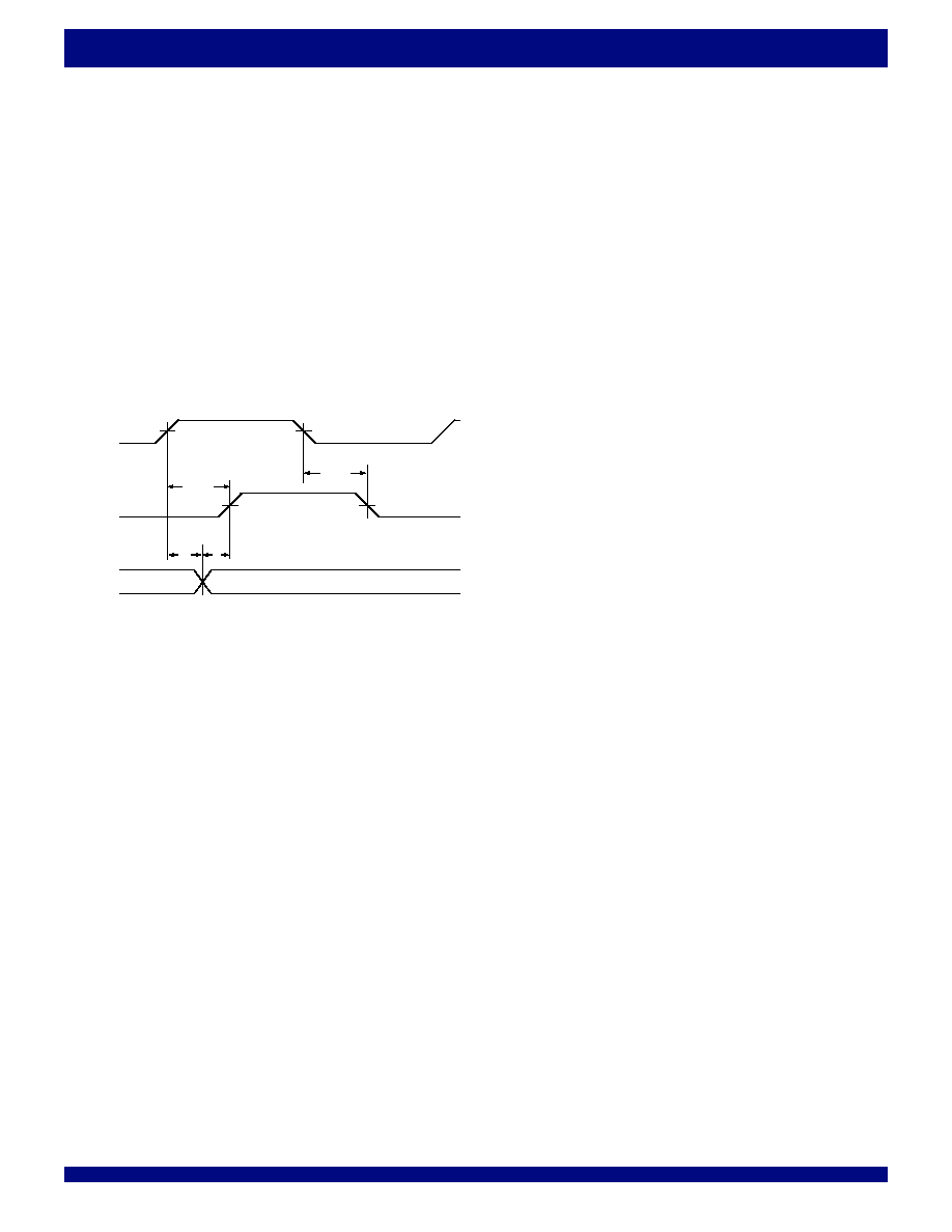
31
IDT72T51546/72T51556 2.5V, MULTI-QUEUE FLOW-CONTROL DEVICES
(32 QUEUES) 36 BIT WIDE CONFIGURATION 1,179,648 and 2,359,296 bits
COMMERCIAL AND INDUSTRIAL
TEMPERATURE RANGES
ECHO READ CLOCK (ERCLK)
The Echo Read Clock output is provided in both HSTL and LVTTL mode,
selectable via IOSEL. The ERCLK is a free-running clock output, it will always
follow the RCLK input regardless of
REN and RADEN.
The ERCLK output follows the RCLK input with an associated delay. This
delay provides the user with a more effective read clock source when reading
data from the Qn outputs. This is especially helpful at high speeds when
variables within the device may cause changes in the data access times. These
variations in access time maybe caused by ambient temperature, supply
voltage, device characteristics. The ERCLK output also compensates for any
trace length delays between the Qn data outputs and receiving devices inputs.
Any variations effecting the data access time will also have a corresponding
effect on the ERCLK output produced by the Queue device, therefore the
ERCLK output level transitions should always be at the same position in time
relative to the data outputs. Note, that ERCLK is guaranteed by design to be
slower than the slowest Qn, data output. Refer to Figure 3, Echo Read Clock
and Data Output Relationship and Figure 27, Echo RCLK & Echo
REN
Operation for timing information.
ECHO READ ENABLE (
EREN)
The Echo Read Enable output is provided in both HSTL and LVTTL mode,
selectable via IOSEL.
The
EREN output is provided to be used in conjunction with the ERCLK
output and provides the reading device with a more effective scheme for reading
data from the Qn output port at high speeds. The
EREN output is controlled by
internal logic that behaves as follows: The
EREN output is active LOW for the
RCLK cycle that a new word is read out of the Queue. That is, a rising edge
of RCLK will cause
EREN to go active (LOW) if REN is active and the Queue
is NOT empty.
Figure 3. Echo Read Clock and Data Output Relationship
NOTES:
1.
REN is LOW. OE is LOW.
2. t
ERCLK
> t
A
, guaranteed by design.
3. Qslowest is the data output with the slowest access time, t
A
.
4. Time, t
D
is greater than zero, guaranteed by design.
5998 drw08
ERCLK
t
A
t
D
Q
SLOWEST
(3)
RCLK
t
ERCLK
t
ERCLK
32
COMMERCIAL AND INDUSTRIAL
TEMPERATURE RANGES
IDT72T51546/72T51556 2.5V, MULTI-QUEUE FLOW-CONTROL DEVICES
(32 QUEUES) 36 BIT WIDE CONFIGURATION 1,179,648 and 2,359,296 bits
D
B
C
A
(c) x36 INPUT to x9 OUTPUT
1st: Read from Queue
2nd: Read from Queue
3rd: Read from Queue
4th: Read from Queue
5998 drw09
Q35-Q27 Q26-Q18 Q17-Q9 Q8-Q0
Q35-Q27 Q26-Q18 Q17-Q9 Q8-Q0
Q35-Q27 Q26-Q18 Q17-Q9 Q8-Q0
Q35-Q27 Q26-Q18 Q17-Q9 Q8-Q0
A
C
B
B
D
A
C
D
(a) x36 INPUT to x36 OUTPUT
(b) x36 INPUT to x18 OUTPUT
Read from Queue
L
BM
IW
OW
L
L
1st: Read from Queue
2nd: Read from Queue
BYTE ORDER ON OUTPUT PORT:
Q35-Q27 Q26-Q18 Q17-Q9 Q8-Q0
Q35-Q27 Q26-Q18 Q17-Q9 Q8-Q0
Q35-Q27 Q26-Q18 Q17-Q9 Q8-Q0
A
C
B
D
1st: Write to Queue
2nd: Write to Queue
3rd: Write to Queue
4th: Write to Queue
BYTE ORDER ON INPUT PORT:
D
C
B
A
(e) x9 INPUT to x36 OUTPUT
Read from Queue
BYTE ORDER ON OUTPUT PORT:
D35-D27 D26-D18 D17-D9 D8-D0
D35-D27 D26-D18 D17-D9 D8-D0
D35-D27 D26-D18 D17-D9 D8-D0
D35-D27 D26-D18 D17-D9 D8-D0
Q35-Q27 Q26-Q18 Q17-Q9 Q8-Q0
Q35-Q27 Q26-Q18 Q17-Q9 Q8-Q0
C
A
D
D
B
C
A
B
D35-D27 D26-D18 D17-D9 D8-D0
(d) x18 INPUT to x36 OUTPUT
Read from Queue
BYTE ORDER ON INPUT PORT:
D35-D27 D26-D18 D17-D9 D8-D0
1st: Write to Queue
2nd: Write to Queue
BYTE ORDER ON OUTPUT PORT:
D35-D27 D26-D18 D17-D9 D8-D0
A
B
C
D
Write to Queue
BYTE ORDER ON INPUT PORT:
H
BM
IW
OW
L
L
H
BM
IW
OW
L
H
H
BM
IW
OW
H
L
H
BM
IW
OW
H
H
Figure 4. Bus-Matching Byte Arrangement
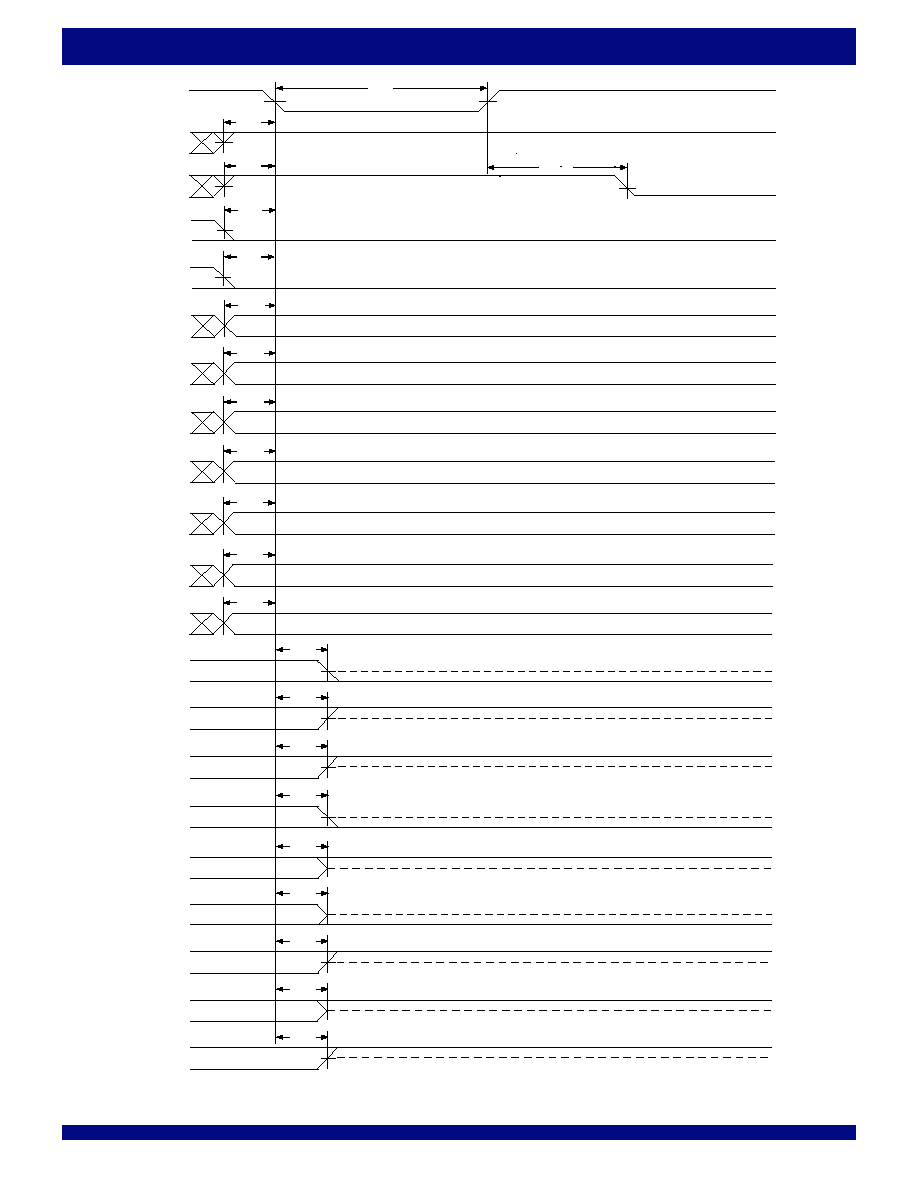
33
IDT72T51546/72T51556 2.5V, MULTI-QUEUE FLOW-CONTROL DEVICES
(32 QUEUES) 36 BIT WIDE CONFIGURATION 1,179,648 and 2,359,296 bits
COMMERCIAL AND INDUSTRIAL
TEMPERATURE RANGES
OV
t
RSF
PAF
t
RSF
PAE
t
RSF
t
RSF
t
RSF
PR
t
RSF
t
RSF
Qn
t
RSF
LOGIC "1" if
OE is LOW and device is Master
HIGH-Z if
OE is HIGH or Device is Slave
LOGIC "1" if Master Device
HIGH-Z if Slave Device
LOGIC "1" if Master Device
HIGH-Z if Slave Device
HIGH-Z if Slave Device
LOGIC "0" if Master Device
HIGH-Z if Slave Device
LOGIC "0" if Master Device
LOGIC "1" if Master Device
HIGH-Z if Slave Device
LOGIC "1" if Master Device
HIGH-Z if Slave Device
LOGIC "1" if Master Device
HIGH-Z if Slave Device
PAFn
PAEn
PRn
t
RS
MRS
WEN
REN
t
RSS
FSTR,
ESTR
5998 drw10
t
RSR
SENI
WADEN,
RADEN
t
RSS
t
RSS
t
RSS
OW, IW,
BM
DF
FM
HIGH = Looped
LOW = Strobed (Direct)
ID0, ID1,
ID2
t
RSS
HIGH = Packet Ready Mode
LOW = Almost Empty
MAST
PKT
DFM
HIGH = Master Device
LOW = Slave Device
HIGH = Default Programming
LOW = Serial Programming
HIGH = Offset Value is 128
LOW = Offset value is 8
t
RSS
t
RSS
t
RSS
t
RSS
t
RSS
t
RSS
FF
t
RSF
HIGH-Z if Slave Device
LOGIC "0" if Master Device
Figure 5. Master Reset
NOTES:
1.
OE can toggle during this period.
2.
PRS should be HIGH during a MRS.
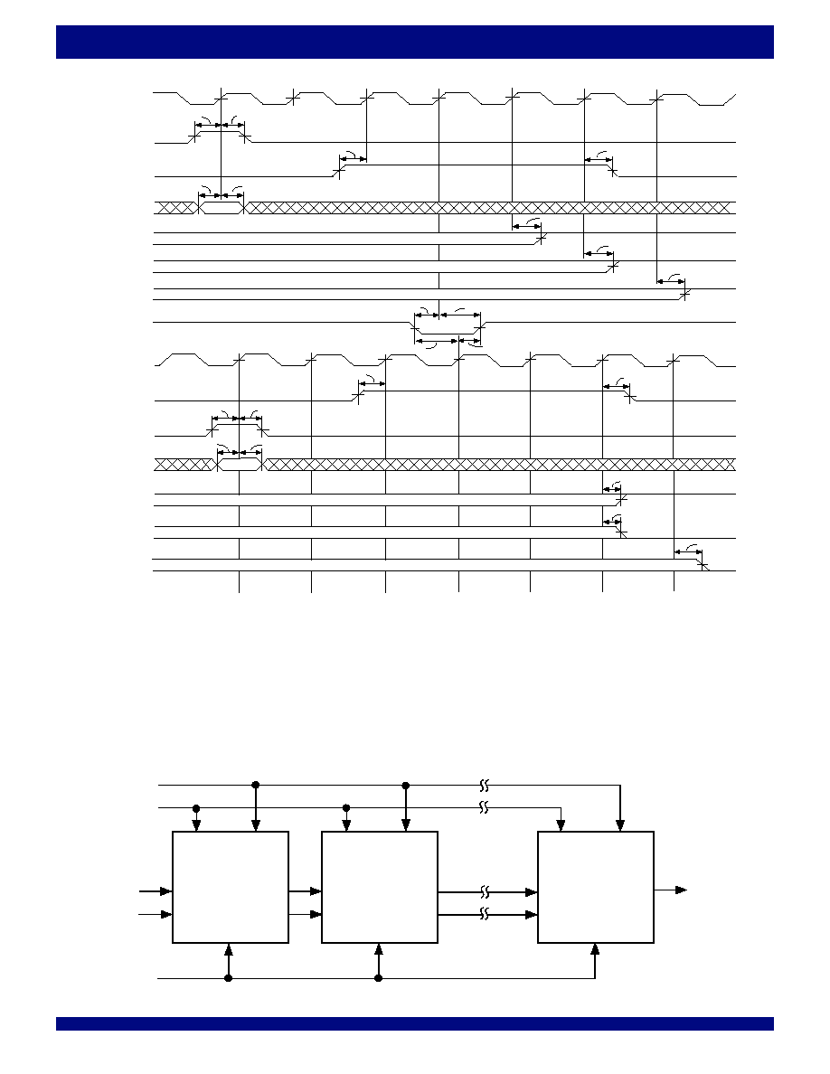
34
COMMERCIAL AND INDUSTRIAL
TEMPERATURE RANGES
IDT72T51546/72T51556 2.5V, MULTI-QUEUE FLOW-CONTROL DEVICES
(32 QUEUES) 36 BIT WIDE CONFIGURATION 1,179,648 and 2,359,296 bits
Figure 7. Serial Port Connection for Serial Programming
DFM
MRS
SENI
SENO
MQ1
SI
SO
SCLK
DFM
MRS
SENI
SENO
MQ2
SI
SO
SCLK
DFM
MRS
SENI
SENO
MQn
SI
SO
SCLK
Serial Enable
Serial Input
Serial Clock
Default Mode
DFM = 0
Master Reset
Serial Loading
Complete
5998 drw12
Figure 6. Partial Reset
NOTES:
1. For a Partial Reset to be performed on a Queue, that Queue must be selected on both the write and read ports.
2. The queue must be selected a minimum of 3 clock cycles before the Partial Reset takes place, on both the write and read ports.
3. The Partial Reset must be LOW for a minimum of 1 WCLK and 1 RCLK cycle.
4. Writing or Reading to the queue (or a queue change) cannot occur until a minimum of 3 clock cycles after the Partial Reset has gone HIGH, on both the write and read ports.
5. The
PAF flag output for Qx on the PAFn flag bus may update one cycle later than the active PAF flag.
6. The
PAE flag output for Qx on the PAEn flag bus may update one cycle later than the active PAE flag.
WCLK
RCLK
RDADD
t
AH
t
AS
t
QH
t
QS
Qx
RADEN
r-2
r-1
r
t
PRSH
t
PRSS
t
PRSH
t
PRSS
PRS
r+3
r+1
t
ENS
REN
r+4
t
ENS
t
ROV
OV
t
RAE
PAE
5998 drw11
t
ENS
w+1
w+2
w+3
t
WFF
t
WAF
t
PAF
WEN
WADEN
t
AH
t
AS
WRADD
Qx
w-3
w-2
w-1
t
QH
t
QS
t
ENS
FF
PAF
Active Bus
PAF-Qx
(5)
Active Bus
PAE-Qx
(6)
t
PAE
w
r+2
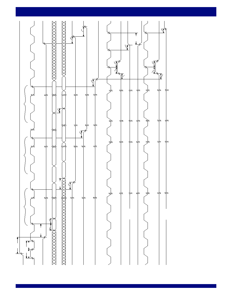
35
IDT72T51546/72T51556 2.5V, MULTI-QUEUE FLOW-CONTROL DEVICES
(32 QUEUES) 36 BIT WIDE CONFIGURATION 1,179,648 and 2,359,296 bits
COMMERCIAL AND INDUSTRIAL
TEMPERATURE RANGES
Figure 8. Serial Programming
RCLK
WEN
SENO (M
Q1)
FF
WADEN/
FSTR
RADEN/
ESTR
OV
WCLK
5998 drw13
t
WFF
t
ENS
t
ROV
t
PCWQ
t
QS
t
QH
t
QS
t
QH
t
PCRQ
HIGH - Z
HIGH - Z
(Slave Device)
(Slave Device)
SO
(
M
Q1)
MRS
SCLK
SENI
(
M
Q1)
SI
(
M
Q1)
t
RSR
t
SENO
1st
2nd
nth
1st
2nd
nth
1st
2nd
nth
t
SENS
SENO (M
Q2)
SENO (M
Q8)
B
12
B
11
t
SDS
B
1n
t
SDH
B
21
B
22
B
2n
B
81
B
82
B
8n
B
21
B
22
B
2n
B
81
B
82
B
8n
t
SENO
t
SENO
t
SCLK
t
SCKL
t
SCKH
Programming Complete
1st Device in Chain
2nd Device in Chain
Final Device in Chain
t
SDO
t
SDOP
t
SENOP
t
SENOP
NOTES:
1.
SENI
can be toggled during serial loading. Once serial programming of a device is complete, the
SENI
and SI inputs become transparent.
SENI
SENO
and SI
SO.
2
.
DFM is LOW during Master Reset to provide Serial programming mode, DF is don't care.
3
.
When
SENO
of the final device is LOW no further serial loads will be accepted.
4
.
n = 19+(Qx72); where Q is the number of queues required for the IDT72T51546/72T51556.
5
.
This diagram illustrates 8 devices in expansion.
6
.
Programming of all devices must be complete (
SENO
of the final device is LOW), before any write or read port operations can take place, this includes queue selections.
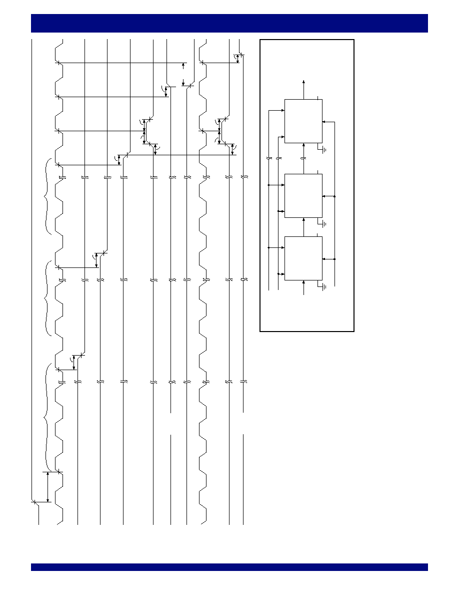
36
COMMERCIAL AND INDUSTRIAL
TEMPERATURE RANGES
IDT72T51546/72T51556 2.5V, MULTI-QUEUE FLOW-CONTROL DEVICES
(32 QUEUES) 36 BIT WIDE CONFIGURATION 1,179,648 and 2,359,296 bits
Figure 9. Default Programming
DFM
MRS
SENI
SENO
MQ1
WCLK
Serial Enable
(can be tied
LOW)
WCLK
Default Mode
DFM = 1
Master Reset
Serial Loading
Complete
DFM
MRS
SENI
SENO
MQ2
WCLK
DFM
MRS
SENI
S
ENO
MQn
WCLK
RCLK
WEN
FF
WADEN/
FSTR
RADEN/
ESTR
OV
5998 drw14
t
WFF
t
ENS
t
ROV
t
PCWQ
t
QS
t
QH
t
QS
t
QH
t
PCRQ
HIGH - Z
HIGH - Z
(Slave Device)
(Slave Device)
SENO (M
Q1)
t
SENO
SENO (M
Q2)
SENO (M
Q8)
t
SENO
WCLK
MRS
1st Device in Chain
1st
2nd
nth
3rd
2nd Device in Chain
1st
2nd
nth
Final Device in Chain
1st
2nd
nth
Programming
Complete
t
SENO
Serial Port Connection for Default Programming
SI
SO
XS
I
S
O
XS
I
S
O
X
NOTES:
1
.
This diagram illustrates multiple devices connected in expansion.
The
SENO
of the final device in a chain is the "programming complete" signal.
2.
SENI
of the first device in the chain can be held LOW
3
.
The
SENO
of a device should connect to the
SENI
of the next device in the chain.
The final device
SENO
is used to indicate programming complete.
4
.
When Default Programming is complete the
SENO
of the final device will go LOW.
5
.
SCLK is not used and can be tied LOW.
6
.
Programming of all devices must be complete (
SENO
of the final device is LOW),
before any write or read port operations can take place, this includes queue selections.
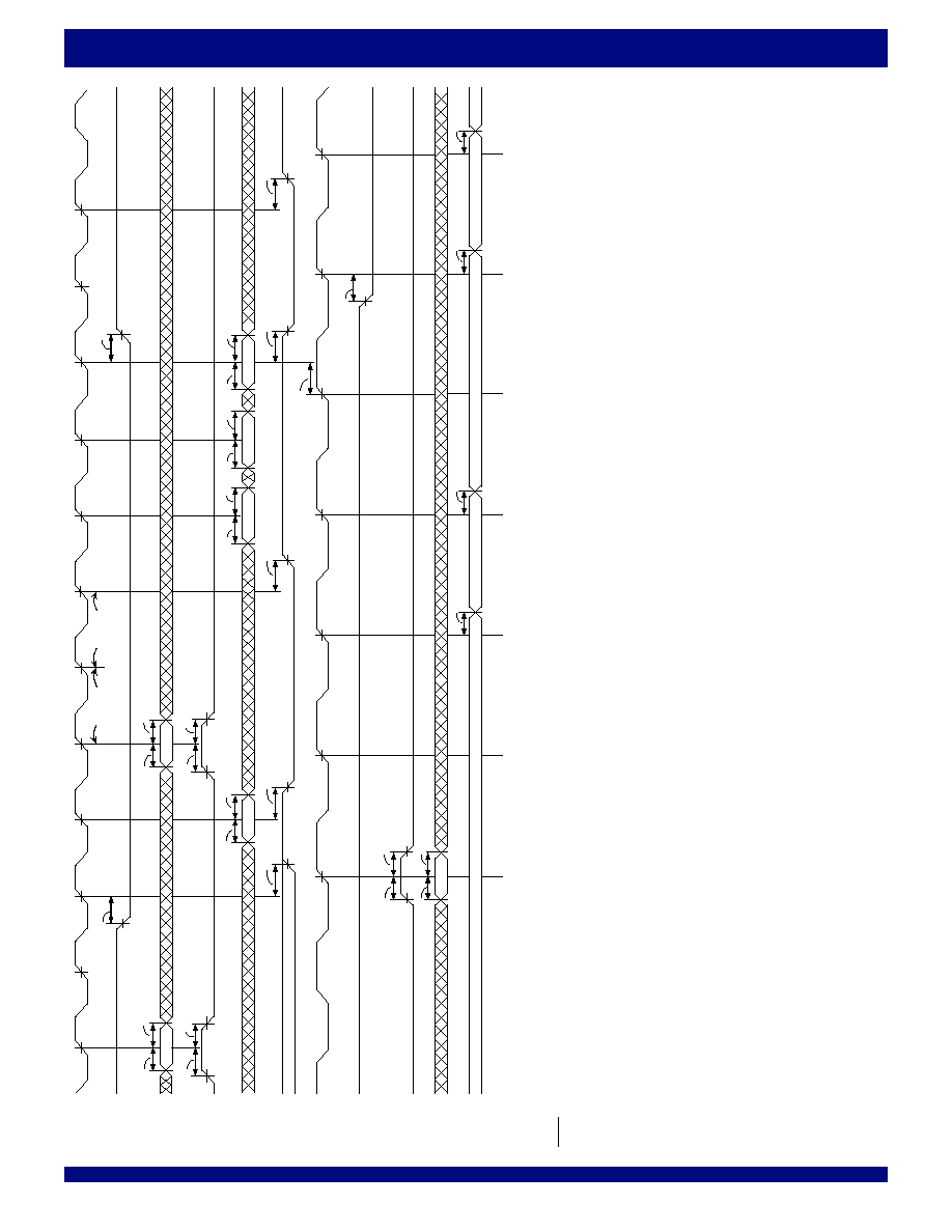
37
IDT72T51546/72T51556 2.5V, MULTI-QUEUE FLOW-CONTROL DEVICES
(32 QUEUES) 36 BIT WIDE CONFIGURATION 1,179,648 and 2,359,296 bits
COMMERCIAL AND INDUSTRIAL
TEMPERATURE RANGES
Figure 10. Write Queue Select, Write Operation and Full Flag Operation
WCLK
5998 drw15
t
SKEW1
t
QS
t
QH
t
ENS
Q
y
t
A
Previous Q, Word, W
Previous Q, W
+1
PFT
t
A
t
A
Qy, W
0
Qy, W
1
t
AS
t
AH
*
A
A*
*BB*
*CC*
*
D
D*
*
E
E*
*
FF*
t
ENS
t
AH
t
AS
Q
y
t
QH
t
QS
t
DH
t
DS
Q
X
W
D
t
DH
Q
y
W
D-2
t
DH
t
DS
Q
y
W
D
t
DS
t
DH
t
DS
t
WFF
t
WFF
t
WFF
No Writes
Queue Full
*C*
*
D*
*E*
*F*
*G*
*
H*
t
ENH
*I*
*J*
*K*
WADEN
t
QH
t
QS
t
AH
t
AS
WRADD
Q
x
FF
WEN
Din
Previous Q Status
*A*
RCLK
REN
RDADD
RADEN
Qout
*B*
t
A
*G
G
*
t
WFF
t
WFF
*L*
No Writes
Queue Full
Q
y
W
D-1
Qy, W
2
12
3
NOTE
:
OE
is active LOW.
Cycle
:
*A*
Queue, Qx is selected on the write port.
The
FF
flag is providing status of a previously selected queue, within the same device.
*AA*
Queue, Qy is selected for read operations.
*B*
The
FF
flag provides status of previous queue for 3 WCLK cycles.
*BB*
Current word is kept on the output bus since
REN
is HIGH.
*C*
The
FF
flag output updates to show the status of Qx, it is not full.
*CC*
Word W+1 is read from the previous queue regardless of
REN
due to FWFT.
*D*
Word, Wd is written into Qx. This causes Qx to go full.
*DD*
The next available Word W0 of Qy is read out regardless of
REN
, 3 RCLK cycles after queue selection. This is FWFT operation.
*E*
Queue, Qy is selected within the same device as Qx. A write to Qx cannot occur on this cycle because it is full,
FF
is LOW.
*EE*
No reads occur,
REN
is HIGH.
*F*
Again, a write to Qx cannot occur on this cycle because it is full,
FF
is LOW.
*FF*
Word, W1 is read from Qy, this causes Qy to go "not full",
FF
flag goes HIGH after time, t
SKEW1
+ t
WFF
. Note, if t
SKEW1
is violated the time
FF
HIGH will be: t
SKEW1
+ WCLK + t
WFF
.
*G*
The
FF
flag updates after time t
WFF
to show that queue, Qy is not full.
*GG*
Word, W2 is read from Qy.
*H*
Word, Wd-2 is written into Qy.
*I*
Word, Wd-1 is written into Qy.
*J*
Word, Wd is written into Qy, this causes Qy to go full,
FF
goes LOW.
*K*
A write to Qy cannot occur on this cycle because it is full,
FF
is LOW.
*L*
Qy goes "not full" based on reading word W1 from Qy on cycle *FF*.
38
COMMERCIAL AND INDUSTRIAL
TEMPERATURE RANGES
IDT72T51546/72T51556 2.5V, MULTI-QUEUE FLOW-CONTROL DEVICES
(32 QUEUES) 36 BIT WIDE CONFIGURATION 1,179,648 and 2,359,296 bits
5998 drw16
W1
W2
W3
WCLK
t
ENH
WEN
Dn
t
DH
t
DS
t
DS
t
DH
t
DS
t
DH
RCLK
t
SKEW1
1
2
t
ENS
REN
t
A
W1 Qy
FWFT
t
A
t
A
W2 Qy
FWFT
W3 Qy
Last Word Read Out of Queue
Qout
t
ROV
OV
t
ROV
t
ENS
Figure 11. Write Operations & First Word Fall Through
NOTES:
1. Qy has previously been selected on both the write and read ports.
2.
OE is LOW.
3. The First Word Latency = t
SKEW1
+ RCLK + t
A
. If t
SKEW1
is violated an additional RCLK cycle must be added.

39
IDT72T51546/72T51556 2.5V, MULTI-QUEUE FLOW-CONTROL DEVICES
(32 QUEUES) 36 BIT WIDE CONFIGURATION 1,179,648 and 2,359,296 bits
COMMERCIAL AND INDUSTRIAL
TEMPERATURE RANGES
WCLK
t
FFLZ
5998 drw17
1
2
t
SKEW1
t
AH
t
AS
D
1
Q
5
t
Q
H
t
QS
t
A
Previous Q W
X-1
D
1
-Q
5
Word W
0
PFT
*
A
A*
*BB*
*CC*
t
ENS
t
AH
t
AS
t
AH
t
AS
t
QH
t
QS
D
2
Q
9
t
QH
t
QS
t
DH
t
DS
W
D
D
1
Q27
t
DH
t
DS
t
WFF
W
D
D
1
Q5
t
WFF
t
WFF
t
ENH
t
ENS
t
ENH
D
1
Q
5
t
FFHZ
t
WFF
HIGH-Z
t
FFHZ
HIGH-Z
t
FFLZ
Addr=001
00101
*C*
*
D*
*E*
*F*
*G*
*
H*
*I*
*
J*
No Write
*K*
WADEN
t
QH
t
QS
t
AH
t
AS
WRADD
D
1
Q
27
FF (Device 1)
WEN
Din
HIGH-Z
RCLK
Addr=001
11011
FF (Device 2)
RDADD
RADEN
*A*
Qout
*B*
*D
D
*
3
t
A
Previous Q W
X
PFT
Figure 12. Full Flag Timing in Expansion Mode
NOTE:
1.
REN
= HIGH.
Cycle
:
*A*
Queue, Q27 of device 1 is selected on the write port.
The
FF
flag of device 1 is in High-Impedance, the write port of device 2 was previously selected.
WEN
is HIGH so no write occurs.
*AA*
Queue, Q5 of device 1 is selected on the read port.
*B*
The
FF
flag stays in High-Impedance for 2 WCLK cycles.
*BB*
Word, Wx-1 is held on the outputs for 2 RCLK cycles after a read Queue switch.
*C*
The
FF
flag of device 2 goes to High-Impedance and the
FF
flag of device 1 goes to Low-Impedance, logic HIGH indicating that D1 Q27 is not full.
WEN
is HIGH so no write occurs.
*CC*
Word, Wx is read from the previously selected queue, (due to FWFT).
*D*
Word, Wd is written into Q27 of D1. This write operation causes Q27 to go full,
FF
goes LOW.
*DD*
The first word from Q5 of D1 selected on cycle *AA* is read out, this occurred regardless of
REN
due to FWFT. This read caused Q5 to go not full, therefore the
FF
flag will go HIGH after: t
SKEW1
+ t
WFF
.
Note if t
SKEW1
is violated the time to
FF
flag HIGH is t
SKEW1
+ WLCK + t
WFF
.
*E*
Queue, Q5 of device 1 is selected on the write port. No write occurs on this cycle.
*F*
The
FF
flag stays in High-Impedance for 2 WCLK cycles.
*G*
The
FF
flag updates to show the status of D1 Q5, it is not full,
FF
goes HIGH.
*H*
Word, Wd is written into Q5 of D1. This causes the queue to go full,
FF
goes LOW.
*I*
No write occurs regardless of
WEN
, the
FF
flag is LOW preventing writes. The
FF
flag goes HIGH due to the read from Q5 of D1 on cycle *CC*.
(This read is not an enabled read, it
is due to the
F
WFT operation
).
*J*
Queue, Q9 of device 2 is selected on the write port.
*K*
The
FF
flag of device 1 goes to High-Impedance, this device was deselected on the write port on cycle *I*. The
FF
flag of device 2 goes to Low-Impedance and provides status of Q9 of D2.

40
COMMERCIAL AND INDUSTRIAL
TEMPERATURE RANGES
IDT72T51546/72T51556 2.5V, MULTI-QUEUE FLOW-CONTROL DEVICES
(32 QUEUES) 36 BIT WIDE CONFIGURATION 1,179,648 and 2,359,296 bits
Figure 13. Read Queue Select, Read Operation
RCLK
5998 drw18
t
AH
t
AS
Q
F
RDADD
t
QH
t
QS
RADEN
REN
t
ENS
t
ENH
t
ENS
t
AH
t
AS
Q
G
t
QH
t
QS
Q
OUT
Q
P
W
n-3
t
A
Q
P
W
n-2
t
A
Previous Q, Q
P
W
n-1
t
A
t
A
Q
P
W
n
t
A
Q
P
W
n+
1
PFT
t
A
Q
F
W
0
Q
F
W
1
t
ROV
OV
Previous Q
1
2
*A*
*
B*
*C*
*
D*
*E*
*F*
*G*
*
H*
PFT
*I*
t
A
Q
F
W
2
*J*
3
Cycle
:
*A*
Word Wn-
3
is read from a previously selected queue Qp on the read port.
*B*
Wn-
2
is read.
*C*
Reads are disabled, Wn-
1
remains on the output bus.
*D*
A new queue, Q
F
is selected for read operations.
*E*
Word Wn-
1
in Qp is read out.
*F*
The next word available in current queue Q
P
, Wn+
1
is read regardless of
REN
due to FWFT.
*G*
The next word available in the new queue, Q
F
-W
0
falls through to the output bus, again this is regardless of
REN
. A new queue, Q
G
is selected for read operations. (This queue is an empty queue).
*H*
Word, W
1
is read from Q
F
.
*I*
Word, W
2
is read from Q
F
.
*J*
Word W
2
from Q
F
remains on the output bus because Q
G
is empty. The Output Valid Flag,
OV
goes HIGH to indicate that the current word is not valid, i.e. Q
G
is empty.
W
2
is the last word in Q
G
.
41
IDT72T51546/72T51556 2.5V, MULTI-QUEUE FLOW-CONTROL DEVICES
(32 QUEUES) 36 BIT WIDE CONFIGURATION 1,179,648 and 2,359,296 bits
COMMERCIAL AND INDUSTRIAL
TEMPERATURE RANGES
Figure 14. Output Valid Flag Timing (In Expansion Mode)
5998 drw19
t
AH
t
AS
t
QH
t
QS
t
ROV
D
1
Q
15
t
ROV
t
OVHZ
t
SKEW1
t
AH
t
AS
D
1
Q
15
t
Q
H
t
QS
t
DH
t
DS
D
1
Q
15
W
0
t
A
D
1
Q
30
W
D
Last Word
t
OLZ
t
A
D
1
Q
15
PFT W
e-1
t
A
D
1
Q
15
W
e
Last Word
t
A
W
0
Q
15
D
1
t
OVLZ
t
ROV
t
ROV
t
ENS
t
ENH
*D*
*E*
*F*
*G*
*H*
*I*
*J*
RCLK
RADEN
t
QH
t
QS
t
AH
t
AS
RDADD
D
1
Q
30
OV
(Device 1)
t
ENS
REN
Qout
(Device 1)
HIGH-Z
WCLK
OV
(Device 2)
WRADD
WADEN
Din
WEN
*A*
*B*
*C*
Cycle:
*A* Queue 30 of Device 1 is selected for read operations. The
OV is currently being driven by Device 2, a queue within device 2 is selected for reads. Device 2 also has control
of Qout bus, its Qout outputs are in Low-Impedance. This diagram only shows the Qout outputs of device 1. (Reads are disabled).
*B* Reads are now enabled. A word from the previously selected queue of Device 2 will be read out.
*C* After a queue switch, there is a 3 RCLK latency for output data.
*D* The Qout of Device 1 goes to Low-Impedance and word Wd is read from Q30 of D1. This happens to be the last word of Q30. Device 2 places its Qout outputs into
High-Impedance, device 1 has control of the Qout bus. The
OV flag of Device 2 goes to High-Impedance and Device 1 takes control of OV. The OV flag of Device 1 goes LOW
to show that Wd of Q30 is valid.
*E* Queue 15 of device 1 is selected for read operations. The last word of Q30 was read on the previous cycle, therefore
OV goes HIGH to indicate that the data on the Qout is
not valid (Q30 was read to empty). Word, Wd remains on the output bus.
*F* The last word of Q30 remains on the Qout bus,
OV is HIGH, indicating that this word has been previously read.
*G* The next word (We-1), available from the newly selected queue, Q15 of device 1 is now read out. This will occur regardless of
REN, 2 RCLK cycles after queue selection
due to the FWFT operation. The
OV flag updates 3 RCLK cycles after a queue selection.
*H* The last word, We is read from Q15, this queue is now empty.
*I* The
OV flag goes HIGH to indicate that Q15 was read to empty on the previous cycle.
*J* Due to a write operation the
OV flag goes LOW and data word W0 is read from Q15. The latency is: t
SKEW1
+ 1*RCLK + t
ROV
.
42
COMMERCIAL AND INDUSTRIAL
TEMPERATURE RANGES
IDT72T51546/72T51556 2.5V, MULTI-QUEUE FLOW-CONTROL DEVICES
(32 QUEUES) 36 BIT WIDE CONFIGURATION 1,179,648 and 2,359,296 bits
Figure 15. Read Queue Selection with Reads Disabled
RCLK
5998 drw20
t
ENS
t
AH
t
AS
Q
P
t
Q
H
t
QS
t
A
Q
n
W
X+
1
t
A
Q
P
W
D+
3
t
A
t
ENH
Q
n
W
X
t
AH
t
AS
Q
n
RDADD
t
QH
t
QS
RADEN
REN
Q
OUT
Q
P
W
D
t
A
Q
P
W
D+
1
t
A
Q
P
W
D+
2
OV
t
ENS
t
ENH
*A*
*
B*
*C*
*
D*
*E*
*F*
*G*
*H*
*
I*
*J*
*K*
*L*
Q
n
W
X+
2
t
A
t
ENS
t
ENH
12
3
Q
P
W
D+
3
t
A
12
3
Cycle
:
*A*
Word Wd+1 is read from the previously selected queue, Qp.
*B*
Reads are disabled, word Wd+1 remains on the output bus.
*C*
A new queue, Qn is selected for read port operations.
*D*
Word, W
D
+2 of Qp is read out.
*E*
Word W
D
+3 of Qp is read out regardless of
REN
due to FWFT operation.
*F*
The next available word Wx of Qn is read out regardless of
REN
, 3 RCLK cycles after queue selection. This is FWFT operation.
*G*
The queue, Qp is again selected.
*H*
Current Word is kept on the output bus since
REN
is HIGH.
*I*
Word Wx+2 is read from Qn. This is read out regardless of
REN
due to FWFT operation.
*J*
Word W
D
+3 is read from Qp.
*K*
Word W
D
+4 is read from Qp.
*L*
Reads are disabled on this cycle, therefore no further reads occur.
43
IDT72T51546/72T51556 2.5V, MULTI-QUEUE FLOW-CONTROL DEVICES
(32 QUEUES) 36 BIT WIDE CONFIGURATION 1,179,648 and 2,359,296 bits
COMMERCIAL AND INDUSTRIAL
TEMPERATURE RANGES
Figure 16. Read Queue Select, Read Operation and
OE
Timing
RCLK
5998 drw21
t
A
Q
A
W
0
PFT
t
A
t
A
t
ENS
t
AH
t
AS
Q
B
t
QH
t
QS
t
A
t
A
Q
A
W
1
t
ROV
*D*
*F*
*G*
*E*
*I*
*
J*
*H*
t
ENH
t
ENS
Q
A
W
2
Q
A
W
3
Q
A
W
4
t
OHZ
RADEN
t
QH
t
QS
t
AH
t
AS
RDADD
Q
A
OV
Qout
t
OLZ
REN
OE
t
OE
Previous Data in O/P Register
*B*
*A*
*C*
t
ROV
No Read
Q
B
is Empty
*K*
12
3
12
3
t
A
NOTES:
1
.
The Output Valid flag,
OV
is HIGH therefore the previously selected queue has been read to empty. The Output Enable input is Asynchronous, therefore the
Qout output bus will go to Low-Impedance after time t
OLZ
.
The data currently on the output register will be available on the output after time t
OE
. This data is the previous data on the output register, this is the last word read out of the previous queue.
2
.
In expansion mode the
OE
inputs of all devices should be connected together. This allows the output busses of all devices to be High-Impedance controll
ed.
Cycle
:
*A*
Queue A is selected for reads. No data will fall through on this cycle, the previous queue was read to empty.
*B*
No data will fall through on this cycle, the previous queue was read to empty.
*C*
Previous data kept on output bus since there is no read operation.
*D*
Word, W0 from Q
A
is read out regardless of
REN
due to FWFT operation. The
OV
flag goes LOW indicating that Word W0 is valid.
*E*
Reads are disabled therefore word, W0 of Q
A
remains on the output bus.
*F*
Reads are again enabled so word W1 is read from Q
A
.
*G*
Word W2 is read from Q
A
.
*H*
Queue, Q
B
is selected on the read port. This queue is actually empty. Word, W3 is read from Q
A
.
*I*
Word, W4 is read from Q
A
.
*J*
Output Enable is taken HIGH, this is Asynchronous so the output bus goes to High-Impedance after time, t
OHZ
.
*K*
Output Valid flag,
OV
goes HIGH to indicate that Q
B
is empty. Data on the output port is no longer valid.
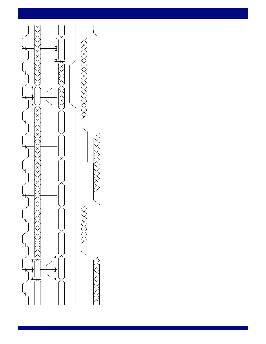
44
COMMERCIAL AND INDUSTRIAL
TEMPERATURE RANGES
IDT72T51546/72T51556 2.5V, MULTI-QUEUE FLOW-CONTROL DEVICES
(32 QUEUES) 36 BIT WIDE CONFIGURATION 1,179,648 and 2,359,296 bits
Figure 17. Writing in Packet Mode during a Queue change
NOTE:
1
.
Do not Write an SOP or EOP on "D" or "K". A filler word is needed.
WCLK
Q
A
WRADD
Q
B
A
Q
C
W
A
DEN
Din
Q
A
Data
Q
A
Data
Q
A
TEOP
Q
A
Dumm
y
Q
B
TSOP
Q
B
Dumm
y
Q
C
TSOP
Q
B
Data
Q
B
Data
WEN
TEOP
(D
3
5
)
TSOP
(D
3
5
)
Q
B
T
EOP
BC
D
(1)
EF
G
H
I
J
t
AS
t
AH
t
AS
t
AH
t
DS
t
DH
t
DS
t
DH
12
12
K
(1)
5998 drw22

45
IDT72T51546/72T51556 2.5V, MULTI-QUEUE FLOW-CONTROL DEVICES
(32 QUEUES) 36 BIT WIDE CONFIGURATION 1,179,648 and 2,359,296 bits
COMMERCIAL AND INDUSTRIAL
TEMPERATURE RANGES
Figure 18. Reading in Packet Mode during a Queue change
NOTE:
1
.
Do not Read an SOP or EOP on "E" or "L". A filler word is needed.
RCLK
Q
A
RD
ADD
Q
B
A
Q
C
RADEN
Qout
Q
A
Data
Q
A
Data
Q
A
REOP
Q
A
"D
u
m
my
"
Q
B
RSOP
Q
B
"D
u
m
my
"
Q
B
Data
Q
B
Data
REN
REOP
(Q
3
5
)
RSOP
(
Q
34)
Q
B
R
EOP
BC
D
E
(1)
FG
H
I
J
K
L
(1)
Q
C
RSOP
t
AS
t
AH
t
AS
t
AH
12
12
t
A
t
A
t
A
t
A
t
A
t
A
t
A
t
A
5998 drw23
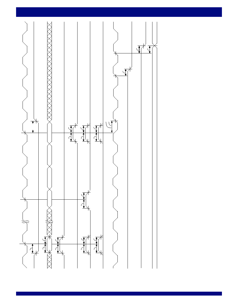
46
COMMERCIAL AND INDUSTRIAL
TEMPERATURE RANGES
IDT72T51546/72T51556 2.5V, MULTI-QUEUE FLOW-CONTROL DEVICES
(32 QUEUES) 36 BIT WIDE CONFIGURATION 1,179,648 and 2,359,296 bits
t
DH
t
DH
t
ENS
*A*
*B*
t
ENH
P1Wo
P1Wn
P1Wn
-1
P1Wn
-2
P1Wn
-3
t
DH
t
DH
t
DH
t
DH
t
DH
t
DH
*C*
t
DS
WCLK
TSOP
(
D34)
RCLK
TEOP
(
D35)
PR
t
PR
WEN
D0-
D31
TAEOP/ TMOD1
(
D33)
TMOD2
(
D32)
5998 drw24
OV
t
ROV
Qn
t
A
P1Wo
t
SKEW5
Last Word Read Out
t
SKEW4
t
DS
t
DS
t
DS
t
DS
t
DS
t
DS
t
DS
Figure 19. Data Input (Transmit) Packet Mode of Operation
NOTES:
1.
REN
is HIGH.
2
.
If t
SKEW4
is violated
PR
may take one additional RCLK cycle.
3
.
If t
SKEW5
is violated the
OV
may take one additional RCLK cycle.
4.
PR
will always go LOW on the same cycle or 1 cycle ahead of
OV
going LOW, (assuming the last word of the packet is the last word in the queue).
5
.
In Packet mode, words cannot be read from a queue until a complete packet has been written into that queue, regardless of
REN
.
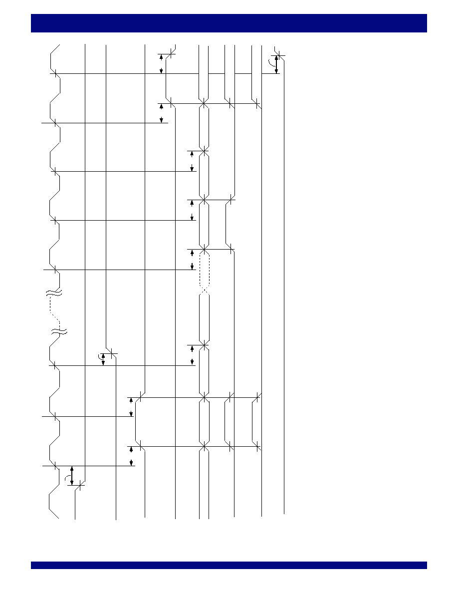
47
IDT72T51546/72T51556 2.5V, MULTI-QUEUE FLOW-CONTROL DEVICES
(32 QUEUES) 36 BIT WIDE CONFIGURATION 1,179,648 and 2,359,296 bits
COMMERCIAL AND INDUSTRIAL
TEMPERATURE RANGES
RSOP
(
Q34)
REOP
(
Q35)
t
PR
t
A
t
ENS
REN
Q0-Q31
P1Wo
P1Wn
P1W1
RAEOP/ RMOD1
(
Q33)
PR
RMOD2
(
Q32)
RCLK
P1Wn
-1
P1Wn
-2
P1Wn
-3
*A*
*B*
*D*
*E*
5998 drw35
OV
t
RO
V
t
A
t
A
t
A
t
A
t
A
t
A
t
A
P1W2
*C*
Figure 20. Data Output (Receive) Packet Mode of Operation
NOTE:
1
.
In Packet mode, words cannot be read from a queue until a complete packet has been written into that queue, regardless of
REN
.
2
.
The
PR
flag will go HIGH on cycle *C* regardless of
REN
.
3
.
The
OV
flag will go HIGH (preventing further reads), when the last complete packet has been read out. If there is a partial packet (a
n incomplete packet) in the queue the
OV
flag will remain HIGH until further writes have
completed the packet.
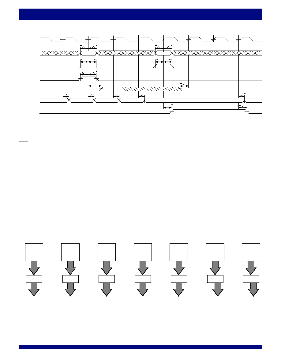
48
COMMERCIAL AND INDUSTRIAL
TEMPERATURE RANGES
IDT72T51546/72T51556 2.5V, MULTI-QUEUE FLOW-CONTROL DEVICES
(32 QUEUES) 36 BIT WIDE CONFIGURATION 1,179,648 and 2,359,296 bits
RCLK
RADEN
Qout
REN
t
AH
t
AS
00100000
RDADD
t
A
NULL QUEUE
SELECT
*A*
*B*
*C*
*E*
*G*
t
A
Q4 W0
FWFT
t
ROV
5998 drw26
t
QH
t
ENS
Q1 Wn-4
Q1 Wn-3
Q1 Wn-2
t
A
t
A
Q1 Wn
t
ROV
OV
SELECT
NEW QUEUE
*D*
00000100
t
AH
t
AS
t
QH
t
QS
t
ENH
t
QS
t
AH
t
AS
Null-Q
*F*
Q1 Wn-1
t
A
Figure 21. Read Operation and Null Queue Select
NOTES:
1. The purpose of the Null queue operation is so that the user can stop reading a block (packet) of data from a queue without filling the 2 stage output pipeline with the next words
from that queue.
2. Please see Figure 22, Null Queue Flow Diagram.
Cycle:
*A* Null Q of device 0 is selected, when word Wn-3 from previously selected Q1 is read.
*C*
REN is HIGH and Wn (Last Word of the Packet) of Q1 is pipelined onto the O/P register.
Note: *B* and *C* are a minimum 3 RCLK cycles between queue selects.
*D* The Null Q is seen as an empty Queue on the read side, therefore Wn of Q1 remains in the O/P register and
OV goes HIGH. A new queue, Q4 is selected.
*G* 1st word, W0 of Q4 falls through present on the O/P register after 3 RCLK cycles after the queue select.
Queue 1
Memory
*A*
*B*
Null
Queue
*C*
O/P Reg.
*D*
*E*
*F*
Null
Queue
Q1
Wn
Queue 4
Memory
O/P Reg.
O/P Reg.
O/P Reg.
O/P Reg.
O/P Reg.
Qn
Wn-2
Q1
Wn
Q1
Wn-1
Q1
Wn
Q1
Wn
Q1
Wn
Q1
Wn
Q1
Wn
Q1
Wn
Q4
W0
Q1
Wn
Queue 1
Memory
Null
Queue
5998 drw27
*G*
Queue 4
Memory
O/P Reg.
Q4
W1
Q4
W0
Figure 22. Null Queue Flow Diagram
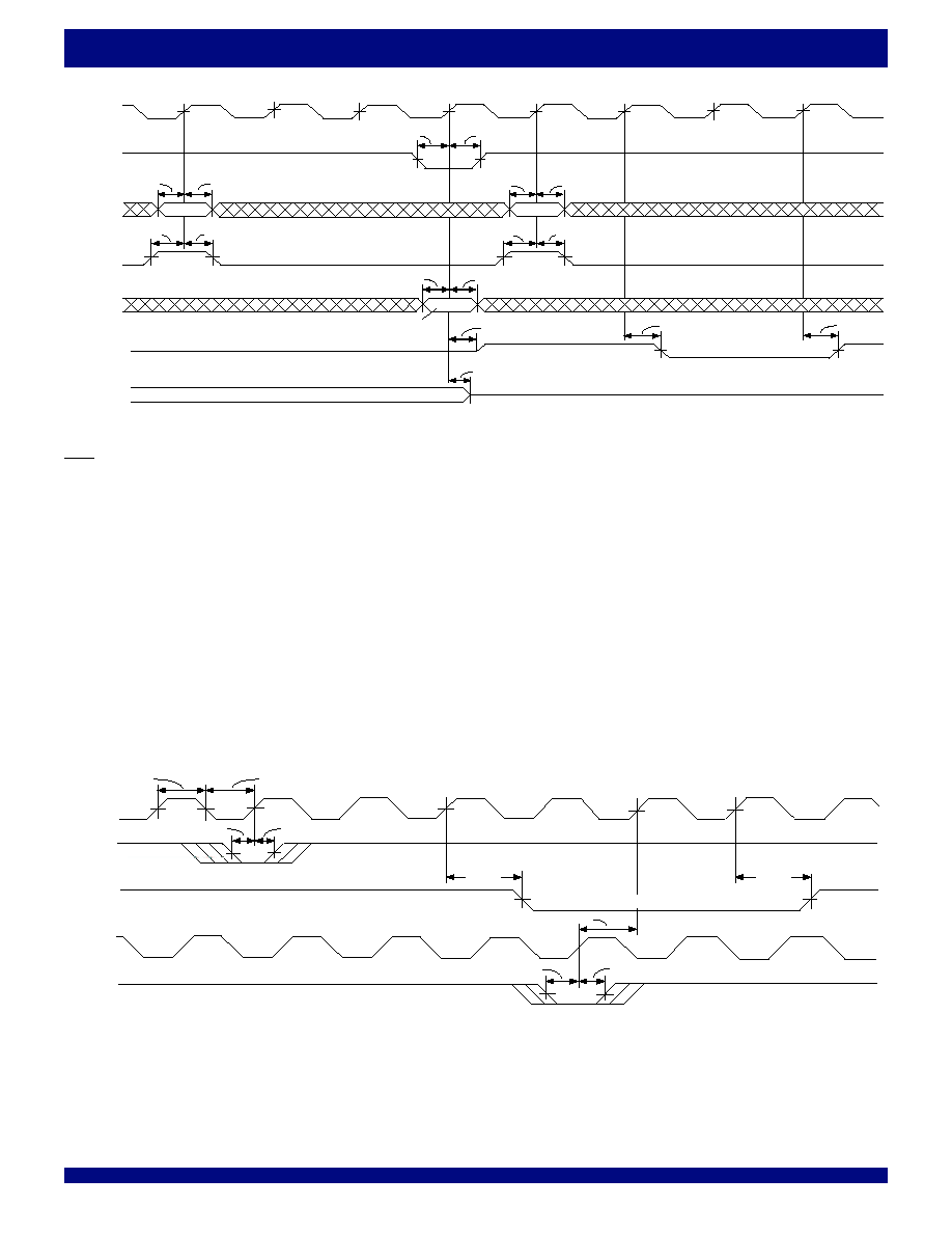
49
IDT72T51546/72T51556 2.5V, MULTI-QUEUE FLOW-CONTROL DEVICES
(32 QUEUES) 36 BIT WIDE CONFIGURATION 1,179,648 and 2,359,296 bits
COMMERCIAL AND INDUSTRIAL
TEMPERATURE RANGES
WCLK
t
AFLZ
5998 drw28
t
ENS
t
AH
t
AS
t
QH
t
QS
t
DH
t
DS
W
D-m
t
WAF
t
WAF
t
ENH
D
1
Q
9
t
FFHZ
1
2
D
1
Q
5
*D*
*F*
*H*
*E*
WADEN
t
QH
t
QS
t
AH
t
AS
WRADD
D
1
Q
5
PAF
(Device 1)
WEN
Din
HIGH-Z
PAF
(Device 2)
*B*
*A*
*C*
*G*
Figure 23. Almost Full Flag Timing and Queue Switch
Figure 24. Almost Full Flag Timing
WCLK
WEN
PAF
RCLK
t
WAF
REN
5998 drw29
D - (m+1) words in Queue
(
2)
D - m words in Queue
1
2
1
D-(m+1) words
in Queue
t
WAF
t
ENH
t
ENS
t
SKEW2
t
ENH
t
ENS
t
CLKL
t
CLKL
Cycle:
*A* Queue 5 of Device 1 is selected on the write port. A queue within Device 2 had previously been selected. The
PAF output of device 1 is High-Impedance.
*B* No write occurs.
*C* No write occurs.
*D* Word, Wd-m is written into Q5 causing the
PAF flag to go from LOW to HIGH. The flag latency is 3 WCLK cycles + t
WAF
.
*E* Queue 9 in device 1 is now selected for write operations. This queue is not almost full, therefore the
PAF flag will update after a 3 WCLK + t
WAF
latency.
*F* The
PAF flag goes LOW based on the write 2 cycles earlier.
*G* No write occurs.
*H* The
PAF flag goes HIGH due to the queue switch to Q9.
NOTE:
1. The waveform here shows the
PAF flag operation when no queue switches are occurring and a queue selected on both the write and read ports is being written to then read
from at the almost full boundary.
Flag Latencies:
Assertion: 2*WCLK + t
WAF
De-assertion: t
SKEW2
+ WCLK + t
WAF
If t
SKEW2
is violated there will be one extra WCLK cycle.
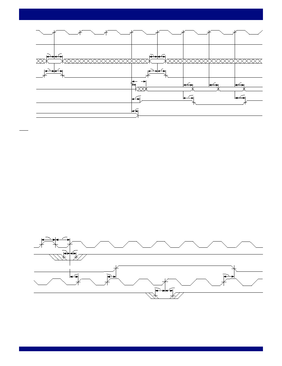
50
COMMERCIAL AND INDUSTRIAL
TEMPERATURE RANGES
IDT72T51546/72T51556 2.5V, MULTI-QUEUE FLOW-CONTROL DEVICES
(32 QUEUES) 36 BIT WIDE CONFIGURATION 1,179,648 and 2,359,296 bits
Figure 25. Almost Empty Flag Timing and Queue Switch
Figure 26. Almost Empty Flag Timing
RCLK
RADEN
t
QH
t
QS
t
AH
t
AS
RDADD
D
1
Q
30
t
AH
t
AS
D
1
Q
15
PAE
(Device 1)
t
AELZ
5998 drw30
t
OLZ
t
RAE
t
RAE
t
AEHZ
t
A
D
1
Q
30
W
n
t
A
D
1
Q
30
W
n+1
t
A
D
1
Q
15
W
0
t
A
D
1
Q
15
W
1
REN
t
QH
t
QS
Qout
HIGH-Z
PAE
(Device 2)
HIGH
HIGH-Z
HIGH-Z
*B*
*C*
*E*
*F*
*D*
*A*
*G*
*H*
WCLK
t
ENH
t
CLKH
t
CLKL
WEN
PAE
RCLK
t
ENS
n+1 words in Queue
t
RAE
t
SKEW2
t
RAE
1
2
REN
5998 drw31
t
ENS
t
ENH
n+2 words in Queue
n+1 words in Queue
Cycle:
*A* Queue 30 of Device 1 is selected on the read port. A queue within Device 2 had previously been selected. The
PAE flag output and the data outputs of device 1 are High-Impedance.
*B* No read occurs.
*C* No read occurs.
*D* The
PAE flag output now switches to device 1. Word, Wn is read from Q30 due to the FWFT operation. This read operation from Q30 is at the almost empty boundary, therefore
PAE will go LOW 2 RCLK cycles later.
*E* Q15 of device 1 is selected.
*F* The
PAE flag goes LOW due to the read from Q30 2 RCLK cycles earlier. Word Wn+1 is read out due to the FWFT operation.
*G* Word, W0 is read from Q15 due to the FWFT operation.
*H* The
PAE flag goes HIGH to show that Q15 is not almost empty.
NOTE:
1. The waveform here shows the
PAE flag operation when no queue switches are occurring and a queue selected on both the write and read ports is being written to then read
from at the almost empty boundary.
Flag Latencies:
Assertion: 2*RCLK + t
RAE
De-assertion: t
SKEW2
+ RCLK + t
RAE
If t
SKEW2
is violated there will be one extra RCLK cycle.
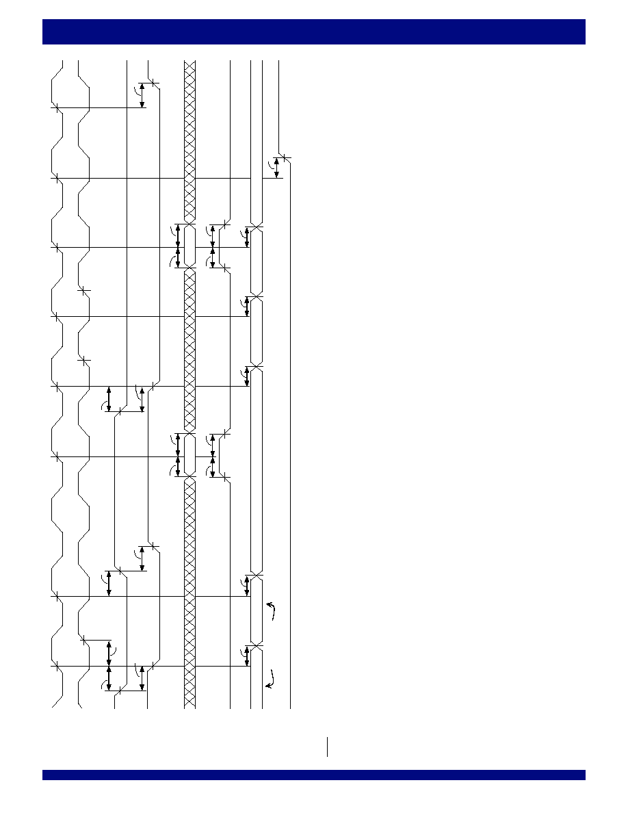
51
IDT72T51546/72T51556 2.5V, MULTI-QUEUE FLOW-CONTROL DEVICES
(32 QUEUES) 36 BIT WIDE CONFIGURATION 1,179,648 and 2,359,296 bits
COMMERCIAL AND INDUSTRIAL
TEMPERATURE RANGES
Figure 27. Echo RCLK and ECHO
REN
Operation
RCLK
1
2
*A*
*
B*
*C*
*D*
*E*
*F*
*G*
*
H*
*I*
5998 drw32
t
AH
t
AS
Q
F
RDADD
t
Q
H
t
QS
RADEN
t
AH
t
AS
Q
G
t
QH
t
QS
Q
OUT
Q
P
W
n-3
t
A
Q
P
W
n-2
t
A
Previous Q, Q
P
W
n-1
t
A
t
A
Q
P
W
n
t
A
PFT
Q
F
W
0
OV
Previous Q
PFT
REN
t
ENS
t
ENH
t
ENS
t
ERCLK
ERCLK
1
2
t
CLKEN
t
CLKEN
EREN
t
CLKEN
t
CLKEN
Q
P
W
n+
1
t
ROV
Cycle
:
*A*
EREN
follow
REN
provided that the current queue (Qp) is not empty.
*B*
EREN
stays active since a new word (Wn-
1
) from Qp is placed on the output bus.
*C, D*
EREN
goes HIGH since no new word has been placed on the output bus on this cycle.
*E*
REN
goes LOW, new word placed on output bus, so
EREN
goes LOW.
*F, G*
EREN
stays active since a new word from Qp has been placed on the output bus.
*H*
W
0
is the last word in Q
F
thus
OV
goes HIGH.
*I*
EREN
goes HIGH since no new word has been placed on the output bus and Q
F
is empty.
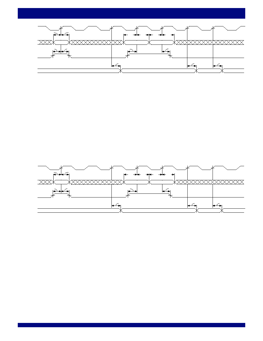
52
COMMERCIAL AND INDUSTRIAL
TEMPERATURE RANGES
IDT72T51546/72T51556 2.5V, MULTI-QUEUE FLOW-CONTROL DEVICES
(32 QUEUES) 36 BIT WIDE CONFIGURATION 1,179,648 and 2,359,296 bits
Figure 28.
PAE
n/
PR
n - Direct Mode - Quadrant Selection
RCLK
t
STH
t
STS
t
QH
t
QS
001xxx10
5998 drw33
t
QS
t
QH
001xxx11
Device 1
Quadrant 3
t
QS
t
QH
001xxx00
Device 1
Quadrant 0
t
STS
t
STH
t
PAE
Device 1 Quadrant 2
t
PAE
Device 1 Quadrant 3
RDADD
ESTR
Device 1
Quadrant 2
PAEn/
PRn
t
PAE
Device 1 Quadrant 0
Figure 29.
PAF
n - Direct Mode - Quadrant Selection
WCLK
5998 drw34
t
QS
t
QH
001xxx11
Device 1
Quadrant 3
t
QS
t
QH
001xxx10
Device 1
Quadrant 2
t
STS
t
STH
t
PAF
t
PAF
Device 1 Quadrant 1
Device 1 Quadrant 2
t
PAF
Device 1 Quadrant 3
t
STH
t
STS
t
QH
t
QS
001xxx01
WRADD
FSTR
Device 1
Quadrant 1
PAFn
NOTES:
1. Quadrants can be selected on consecutive cycles.
2. On an RCLK cycle that the ESTR is HIGH, the RADEN input must be LOW.
3. There is a latency of 2 RCLK for the
PAEn bus to switch.
NOTES:
1. Quadrants can be selected on consecutive cycles.
2. On a WCLK cycle that the FSTR is HIGH, the WADEN input must be LOW.
3. There is a latency of 2 WCLK for the
PAFn bus to switch.
53
IDT72T51546/72T51556 2.5V, MULTI-QUEUE FLOW-CONTROL DEVICES
(32 QUEUES) 36 BIT WIDE CONFIGURATION 1,179,648 and 2,359,296 bits
COMMERCIAL AND INDUSTRIAL
TEMPERATURE RANGES
WCLK
Dn
Prev
PAEn
RCLK
D5 quad 4
101 xxx11
t
AH
1
t
RAE
D5Quad 4
D5Quad 4
t
PAEHZ
t
PAEZL
xxxx xxx1
xxxx xxx1
t
SKEW3
xxxx xxx0
D5Quad4
2
t
STH
t
PAE
5998 drw35
t
RAE
*DD*
*EE*
*GG*
*FF*
xxxx xxx0
D5Quad4
t
ENH
t
ENS
Wy
D5 Q24
Wy+1
D5 Q24
Wy+3
D5 Q24
Wy+2
D5 Q24
Wa+1
D5 Q17
t
A
t
A
t
A
t
A
t
DH
D3Q8
Wn
D5 Q24
Wn+1
D5Q24
011 01000
D4 quad 3
100 xxx10
*D*
*E*
*F*
*G*
t
QH
t
QS
t
AH
t
AS
t
AH
t
AS
t
ENH
t
STH
t
STS
3
t
ENS
t
ENH
t
RAE
D5 Q24
status
ESTR
RDADD
100 11000
D5Q24
t
AS
t
AH
t
AS
Previous value loaded on to PAE bus
RADEN
t
QH
t
QS
t
STS
Device 5
PAE
*AA*
*BB*
D5 Q17 Status
Bus
PAEn
Previous value loaded on to PAE bus
REN
Device 5 -Qn
t
A
Wa
D5 Q17
t
DS
WEN
WADEN
FSTR
t
AH
100 11000
t
AS
WRADD
D5Q24
*A*
*B*
t
QH
t
QS
t
ENS
Device 5
PAEn
1
Wp+1
Wp
Writes to Previous Q
t
DH
t
DS
t
DH
*C*
2
t
QH
t
QS
*H*
Wp+2
t
DS
Wx
D3 Q8
*CC*
3
1
2
3
Figure 30.
PAE
n - Direct Mode, Flag Operation
Cycle:
*A*
Queue 24 of Device 5 is selected for write operations.
Word, Wp is written into the previously selected queue.
*AA* Queue 24 of Device 5 is selected for read operations.
A quadrant from another device has control of the
PAEn bus.
The discrete
PAE output of device 5 is currently in High-Impedance and the PAE active flag is controlled by the previously selected device.
*B*
Word Wp+1 is written into the previously selected queue.
*BB* Current Word is kept on the output bus since
REN is HIGH.
*C*
Word Wp+2 is written into the previously selected queue.
*CC* Word Wa+1 of D5 Q17 is read due to FWFT.
*D*
Word, Wn is written into the newly selected queue, Q24 of D5. This write will cause the
PAE flag on the read port to go from LOW to HIGH (not almost empty) after time,
t
SKEW3
+ RCLK + t
RAE
(if t
SKEW3
is violated one extra RCLK cycle will be added).
*DD* Word, Wy from the newly selected queue, Q24 will be read out due to FWFT operation.
Quadrant 4 of Device 5 is selected on the
PAEn bus. Q24 of device 5 will therefore have is PAE status output on PAE[0]. There is a single RCLK cycle latency before
the
PAEn bus changes to the new selection.
*E*
Queue 8 of Device 3 is selected for write operations.
Word Wn+1 is written into Q24 of D5.
*EE* Word, Wy+1 is read from Q24 of D5.
*F*
No writes occur.
*FF* Word, Wy+2 is read from Q24 of D5.
The
PAEn bus changes control to D5, the PAEn outputs of D5 go to Low-Impedance and quadrant 4 is placed onto the outputs. The device of the previously selected
quadrant now places its
PAEn outputs into High-Impedance to prevent bus contention.
The discrete
PAE flag will go HIGH to show that Q24 of D5 is not almost empty. Q24 of device 5 will have its PAE status output on PAE[0].
*G*
Quadrant 3 of device 4 is selected on the write port for the
PAFn bus.
*GG* The
PAEn bus updates to show that Q24 of D5 is almost empty based on the reading out of word, Wy+1.
The discrete
PAE flag goes LOW to show that Q24 of D5 is almost empty based on the reading of Wy+1.
*H*
Word, Wx is written into Q8 of D3.
54
COMMERCIAL AND INDUSTRIAL
TEMPERATURE RANGES
IDT72T51546/72T51556 2.5V, MULTI-QUEUE FLOW-CONTROL DEVICES
(32 QUEUES) 36 BIT WIDE CONFIGURATION 1,179,648 and 2,359,296 bits
RCLK
OE
*G*
W
D - M + 2
t
A
*I*
t
A
D0 Q31
W
0
D6 Q2
*F*
t
QH
t
QS
D0 Q31
111 xxx00
D7 quad 1
110 00010
*D*
*E*
t
AH
t
AS
t
STH
t
STS
D6Q2
W
D-M+1
t
A
W
X +1
Prev. Q
t
OLZ
REN
RADEN
ESTR
WRADD
t
AH
000 11111
t
AS
RDADD
D0Q31
*A*
*B*
000 xxx11
t
QH
t
QS
t
STH
t
STS
5998 drw36
0xxx xxxx
D0Quad4
*BB*
*CC*
*DD*
*EE*
*FF*
t
PAFLZ
1xxx xxxx
D0Quad4
D0Quad4
t
PAF
t
PAF
0xxx xxxx
0xxx xxxx
D0Quad4
1xxx xxxx
D0Quad4
D0Quad4
0xxx xxxx
t
PAFHZ
HIGH-Z
HIGH-Z
t
PAFLZ
t
WAF
*AA*
Device 0
PAFn
Bus
PAFn
D
X
Quad y
Prev.
PAFn
D
X
Quad y
Device 0
PAF
Qout
W
X
Prev. Q
D0 quad4
FSTR
t
A
WCLK
t
SKEW3
2
3
D0 Q31
WEN
t
ENS
t
ENH
WADEN
t
QH
t
QS
t
AH
t
AS
t
AH
t
AS
Din
t
DS
t
DH
t
DS
t
DH
t
DS
t
DH
Word W
y
D0 Q31
W
y+1
D0 Q31
W
y+2
D0 Q31
*C*
t
AH
t
AS
*H*
1
HIGH - Z
*GG*
Figure 31.
PAF
n - Direct Mode, Flag Operation
Cycle:
*A*
Queue 31 of device 0 is selected for read operations.
The last word in the output register is available on Qout.
OE was previously taken LOW so the output bus is in Low-Impedance.
*AA* Quadrant 4 of device 0 is selected for the
PAFn bus. The bus is currently providing status of a previously selected quadrant, Quad Y of device X.
*B*
No read operation.
*BB* Queue 31 of device 0 is selected on the write port.
*C*
Word, Wx+1 is read out from the previous queue due to the FWFT effect.
*CC*
PAFn continues to show status of Quad4 D0.
The
PAFn bus is updated with the quadrant selected on the previous cycle, D0 Quad 4. PAF[7] is LOW showing the status of queue 31.
The
PAFn outputs of the device previously selected on the PAFn bus go to High-Impedance.
*D*
A new quadrant, Quad 1 of Device 7 is selected for the
PAFn bus.
Word, Wd-m+1 is read from Q31 D0 due to the FWFT operation. This read is at the
PAFn boundary of queue D0 Q31. This read will cause the PAF[7] output to go from
LOW to HIGH (almost full to not almost full), after a delay t
SKEW3
+ WCLK + tPAF. If t
SKEW3
is violated add an extra WCLK cycle.
*DD* No write operation.
*E*
No read operations occur,
REN is HIGH.
*EE*
PAF[7] goes HIGH to show that D0 Q31 is not almost empty due to the read on cycle *C*.
The active queue
PAF flag of device 0 goes from High-Impedance to Low-Impedance.
Word, Wy is written into D0 Q31.
*F*
Queue 2 of Device 6 is selected for read operations.
*FF* Word, Wy+1 is written into D0 Q31.
*G*
Word, Wd-m+2 is read out due to FWFT operation.
*GG*
PAF[7] and the discrete PAF flag go LOW to show the write on cycle *DD* causes Q31 of D0 to again go almost full.
Word, Wy+2 is written into D0 Q31.
*H*
No read operation.
*I*
Word, W0 is read from Q0 of D6, selected on cycle *F*, due to FWFT.
55
IDT72T51546/72T51556 2.5V, MULTI-QUEUE FLOW-CONTROL DEVICES
(32 QUEUES) 36 BIT WIDE CONFIGURATION 1,179,648 and 2,359,296 bits
COMMERCIAL AND INDUSTRIAL
TEMPERATURE RANGES
WCLK
5998 drw37
t
FSYNC
t
FSYNC
FSYNC
0
(MASTER)
FXO
0
/
FXI
1
t
FXO
t
FXO
t
FSYNC
t
FSYNC
FSYNC
1
(SLAVE)
FXO
1
/
FXI
2
t
FXO
t
FXO
t
FSYNC
t
FSYNC
FSYNC
2
(SLAVE)
FXO
2
/
FXI
0
t
FXO
t
FXO
PAF
n
t
PAF
t
PAF
t
PAF
t
PAF
t
PAF
t
PAF
t
PAF
t
PAF
t
PAF
t
PAF
t
PAF
t
PAF
t
PAF
t
PAF
t
FSYNC
t
FSYNC
D0Quad1
D0Quad2
D0Quad3
D0Quad4
D1Quad1
D1Quad2
D1Quad3
D1Quad4
D2Quad1
D2Quad2
D2Quad3
D2Quad4
D0Quad1
D0Quad2
Figure 32.
PAF
n Bus - Polled Mode
NOTE:
1
.
This diagram is based on 3 devices connected in expansion mode.
56
COMMERCIAL AND INDUSTRIAL
TEMPERATURE RANGES
IDT72T51546/72T51556 2.5V, MULTI-QUEUE FLOW-CONTROL DEVICES
(32 QUEUES) 36 BIT WIDE CONFIGURATION 1,179,648 and 2,359,296 bits
RCLK
5998 drw38
t
ESYNC
t
ESYNC
ESYNC
0
EXO
0
/
EXI
1
t
EXO
t
EXO
t
ESYNC
t
ESYNC
ESYNC
1
EXO
1
/
EXI
2
t
EXO
t
EXO
t
ESYNC
t
ESYNC
ESYNC
2
EXO
2
/
EXI
0
t
EXO
t
EXO
PAE
n
t
PAE
t
PAE
t
PAE
t
PAE
t
PAE
t
PAE
t
PAE
t
PAE
t
PAE
t
PAE
t
PAE
t
PAE
t
PAE
t
PAE
t
ESYNC
t
ESYNC
D0Quad1
D0Quad2
D0Quad3
D0Quad4
D1Quad1
D1Quad2
D1Quad3
D1Quad4
D2Quad1
D2Quad2
D2Quad3
D2Quad4
D0Quad1
D0Quad2
Figure 33.
PAE
n/
PR
n Bus - Polled Mode
NOTE:
1
.
This diagram is based on 3 devices connected in expansion mode.
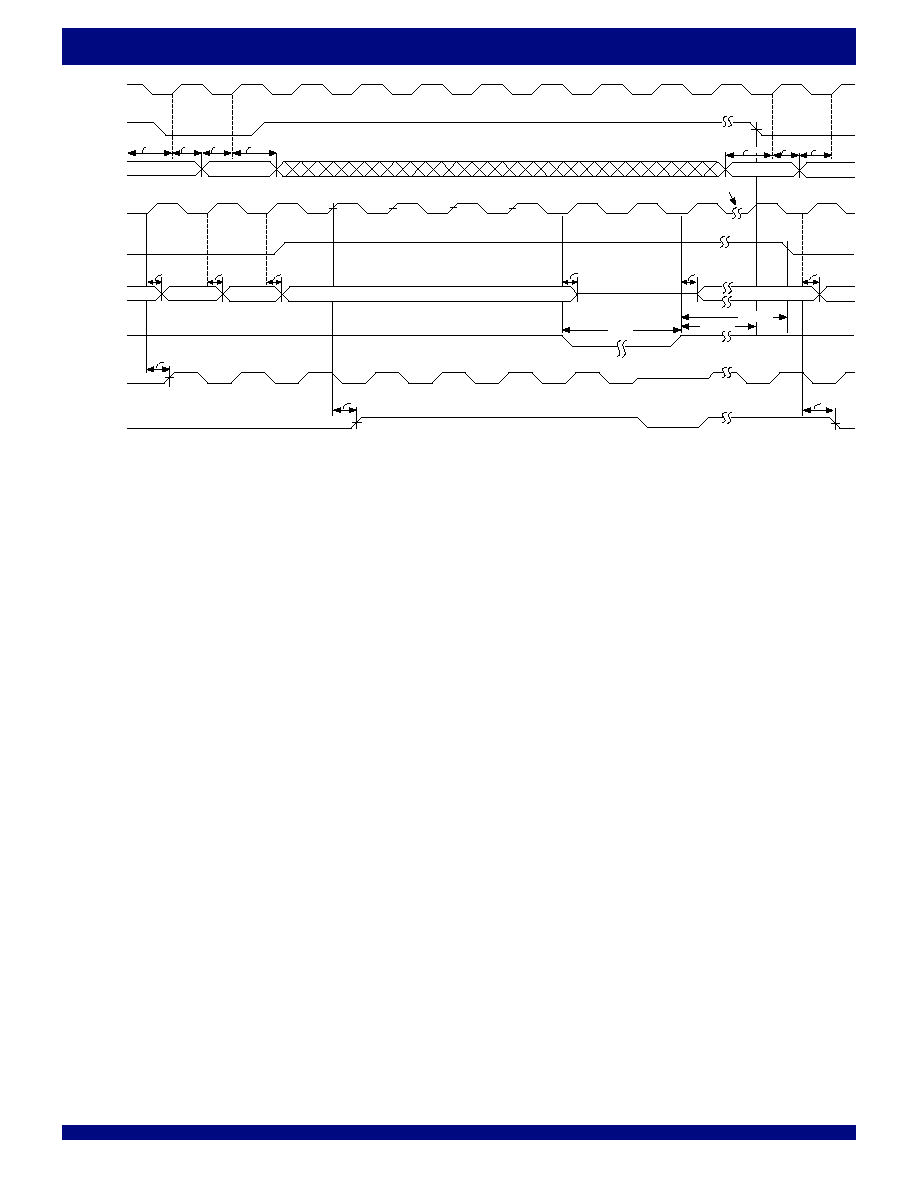
57
IDT72T51546/72T51556 2.5V, MULTI-QUEUE FLOW-CONTROL DEVICES
(32 QUEUES) 36 BIT WIDE CONFIGURATION 1,179,648 and 2,359,296 bits
COMMERCIAL AND INDUSTRIAL
TEMPERATURE RANGES
Figure 34. Power Down Operation
NOTES:
1. All read and write operations must have ceased a minimum of 4 WCLK and 4 RCLK cycles before power down is asserted.
2. When the
PD input becomes deasserted, there will be a 1
Ķs waiting period before read and write operations can resume.
All input and output signals will also resume after this time period.
3. Set-up and configuration static inputs are not affected during power down.
4. Serial programming and JTAG programming port are inactive during power down.
5.
RCS = 0, WCS = 0 and OE = 0. These signals can toggle during and after power down.
6. All flags remain active and maintain their current states.
7. During power down, all outputs will be in high-impedance.
5998 drw39
WCLK
WEN
D[39:0]
RCLK
REN
Q[39:0]
PD
ERCLK
EREN
t
DS
t
DH
t
DH
t
DH
t
DS
1
2
3
4
(1)
t
A
t
A
t
A
t
ERCLK
t
EREN
t
DS
1ns
t
PDHZ
(7)
t
PDLZ
(2)
t
A
t
PDL
t
PDH
(2)
t
PDH
(2)
t
EREN
W
DH
W
DS
Hi-Z
Hi-Z
W
D4
W
D3
W
D2
W
D1
W
D10
W
D11
W
D12
W
D13
t
DS
Hi-Z
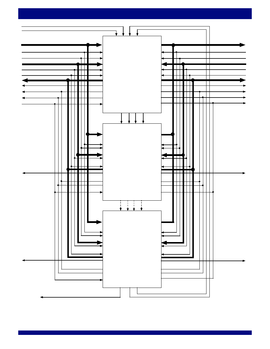
58
COMMERCIAL AND INDUSTRIAL
TEMPERATURE RANGES
IDT72T51546/72T51556 2.5V, MULTI-QUEUE FLOW-CONTROL DEVICES
(32 QUEUES) 36 BIT WIDE CONFIGURATION 1,179,648 and 2,359,296 bits
WRADD
WADEN
WCLK
WEN
FSTR
PAFn
FSYNC
FF
PAF
SCLK
RCLK
REN
ESTR
PAEn
ESYNC
OV
PAE
RDADD
RADEN
SO FXO EXO
SI
FXI
EXI
WRADD
WADEN
WCLK
WEN
FSTR
PAFn
FSYNC
FF
PAF
SCLK
RCLK
REN
ESTR
PAEn
ESYNC
OV
PAE
RDADD
RADEN
SO FXO
EXO
SI FXI
EXI
WRADD
WADEN
WCLK
WEN
FSTR
PAFn
FSYNC
FF
PAF
SCLK
RCLK
REN
ESTR
PAEn
ESYNC
OV
PAE
RDADD
RADEN
SENO
FXO EXO
Q0-Q35
SI
FXI
EXI
Data Bus
Write Clock
Write Enable
Write Queue Select
Full Strobe
Programmable Almost Full
Write Address
Full Sync1
Full Flag
Almost Full Flag
Serial Clock
Output Data Bus
Read Clock
Read Enable
Read Queue Select
Empty Strobe
Programmable Almost Empty
Read Address
Empty Sync 1
Output Valid Flag
Almost Empty Flag
Serial Programming Data Input
DEVICE
1
DEVICE
2
DEVICE
n
Full Sync2
Empty Sync 2
Full Sync n
Empty Sync n
SENO
SENI
DONE
5998 drw40
D0-D35
Q0-Q35
D0-D35
D0-D35
Q0-Q35
SENI
PR
Packet
Reads
PR
PR
Serial Enable
SENO
SENI
Figure 35. Multi-Queue Expansion Diagram
NOTES:
1. If devices are configured for Direct operation of the
PAFn/PAEn flag busses the FXI/EXI of the MASTER device should be tied LOW. All other devices tied HIGH. The FXO/EXO
outputs are DNC (Do Not Connect).
2. Q outputs must not be mixed between devices, i.e. Q0 of device 1 must connect to Q0 of device 2, etc.
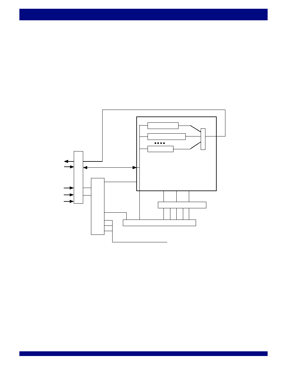
59
IDT72T51546/72T51556 2.5V, MULTI-QUEUE FLOW-CONTROL DEVICES
(32 QUEUES) 36 BIT WIDE CONFIGURATION 1,179,648 and 2,359,296 bits
COMMERCIAL AND INDUSTRIAL
TEMPERATURE RANGES
T
A
P
TAP
Cont-
roller
Mux
DeviceID Reg.
Boundary Scan Reg.
Bypass Reg.
clkDR, ShiftDR
UpdateDR
TDO
TDI
TMS
TCLK
TRST
clklR, ShiftlR
UpdatelR
Instruction Register
Instruction Decode
Control Signals
5998 drw41
JTAG INTERFACE
Five additional pins (TDI, TDO, TMS, TCK and
TRST) are provided to
support the JTAG boundary scan interface. The IDT72T51546/72T51556
incorporates the necessary tap controller and modified pad cells to implement
the JTAG facility.
Note that IDT provides appropriate Boundary Scan Description Language
program files for these devices.
The Standard JTAG interface consists of four basic elements:
∑∑
∑∑
∑
Test Access Port (TAP)
∑∑
∑∑
∑
TAP controller
∑∑
∑∑
∑
Instruction Register (IR)
∑∑
∑∑
∑
Data Register Port (DR)
The following sections provide a brief description of each element. For a
complete description refer to the IEEE Standard Test Access Port Specification
(IEEE Std. 1149.1-1990).
The Figure below shows the standard Boundary-Scan Architecture
Figure 36. Boundary Scan Architecture
TEST ACCESS PORT (TAP)
The Tap interface is a general-purpose port that provides access to the
internal of the processor. It consists of four input ports (TCLK, TMS, TDI,
TRST)
and one output port (TDO).
THE TAP CONTROLLER
The Tap controller is a synchronous finite state machine that responds to
TMS and TCLK signals to generate clock and control signals to the Instruction
and Data Registers for capture and update of data.
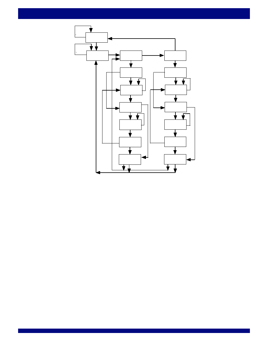
60
COMMERCIAL AND INDUSTRIAL
TEMPERATURE RANGES
IDT72T51546/72T51556 2.5V, MULTI-QUEUE FLOW-CONTROL DEVICES
(32 QUEUES) 36 BIT WIDE CONFIGURATION 1,179,648 and 2,359,296 bits
Test-Logic
Reset
Run-Test/
Idle
1
0
0
Select-
DR-Scan
Select-
IR-Scan
1
1
1
Capture-IR
0
Capture-DR
0
0
EXit1-DR
1
Pause-DR
0
Exit2-DR
1
Update-DR
1
Exit1-IR
1
Exit2-IR
1
Update-IR
1
1
0
1
1
1
5998 drw42
0
Shift-DR
0
0
0
Shift-IR
0
0
Pause-IR
0
1
Input = TMS
0
0
1
Figure 37. TAP Controller State Diagram
NOTES:
1. Five consecutive TCK cycles with TMS = 1 will reset the TAP.
2. TAP controller does not automatically reset upon power-up. The user must provide a reset to the TAP controller (either by
TRST or TMS).
3. TAP controller must be reset before normal Queue operations can begin.
Refer to the IEEE Standard Test Access Port Specification (IEEE Std.
1149.1) for the full state diagram.
All state transitions within the TAP controller occur at the rising edge of the
TCLK pulse. The TMS signal level (0 or 1) determines the state progression
that occurs on each TCLK rising edge. The TAP controller takes precedence
over the Queue and must be reset after power up of the device. See
TRST
description for more details on TAP controller reset.
Test-Logic-Reset All test logic is disabled in this controller state enabling
the normal operation of the IC. The TAP controller state machine is designed
in such a way that, no matter what the initial state of the controller is, the Test-
Logic-Reset state can be entered by holding TMS at high and pulsing TCK five
times. This is the reason why the Test Reset (
TRST) pin is optional.
Run-Test-Idle In this controller state, the test logic in the IC is active only if
certain instructions are present. For example, if an instruction activates the self
test, then it will be executed when the controller enters this state. The test logic
in the IC is idles otherwise.
Select-DR-Scan This is a controller state where the decision to enter the
Data Path or the Select-IR-Scan state is made.
Select-IR-Scan This is a controller state where the decision to enter the
Instruction Path is made. The Controller can return to the Test-Logic-Reset state
other wise.
Capture-IR In this controller state, the shift register bank in the Instruction
Register parallel loads a pattern of fixed values on the rising edge of TCK. The
last two significant bits are always required to be "01".
Shift-IR In this controller state, the instruction register gets connected
between TDI and TDO, and the captured pattern gets shifted on each rising edge
of TCK. The instruction available on the TDI pin is also shifted in to the instruction
register.
Exit1-IR This is a controller state where a decision to enter either the Pause-
IR state or Update-IR state is made.
Pause-IR This state is provided in order to allow the shifting of instruction
register to be temporarily halted.
Exit2-DR This is a controller state where a decision to enter either the Shift-
IR state or Update-IR state is made.
Update-IR In this controller state, the instruction in the instruction register is
latched in to the latch bank of the Instruction Register on every falling edge of
TCK. This instruction also becomes the current instruction once it is latched.
Capture-DR In this controller state, the data is parallel loaded in to the data
registers selected by the current instruction on the rising edge of TCK.
Shift-DR, Exit1-DR, Pause-DR, Exit2-DR and Update-DR These
controller states are similar to the Shift-IR, Exit1-IR, Pause-IR, Exit2-IR and
Update-IR states in the Instruction path.

61
IDT72T51546/72T51556 2.5V, MULTI-QUEUE FLOW-CONTROL DEVICES
(32 QUEUES) 36 BIT WIDE CONFIGURATION 1,179,648 and 2,359,296 bits
COMMERCIAL AND INDUSTRIAL
TEMPERATURE RANGES
THE INSTRUCTION REGISTER
The Instruction register allows an instruction to be shifted in serially into the
processor at the rising edge of TCLK.
The Instruction is used to select the test to be performed, or the test data
register to be accessed, or both. The instruction shifted into the register is latched
at the completion of the shifting process when the TAP controller is at Update-
IR state.
The instruction register must contain 4 bit instruction register-based cells
which can hold instruction data. These mandatory cells are located nearest the
serial outputs they are the least significant bits.
TEST DATA REGISTER
The Test Data register contains three test data registers: the Bypass, the
Boundary Scan register and Device ID register.
These registers are connected in parallel between a common serial input
and a common serial data output.
The following sections provide a brief description of each element. For a
complete description, refer to the IEEE Standard Test Access Port Specification
(IEEE Std. 1149.1-1990).
TEST BYPASS REGISTER
The register is used to allow test data to flow through the device from TDI
to TDO. It contains a single stage shift register for a minimum length in serial path.
When the bypass register is selected by an instruction, the shift register stage
is set to a logic zero on the rising edge of TCLK when the TAP controller is in
the Capture-DR state.
The operation of the bypass register should not have any effect on the
operation of the device in response to the BYPASS instruction.
THE BOUNDARY-SCAN REGISTER
The Boundary Scan Register allows serial data TDI be loaded in to or read
out of the processor input/output ports. The Boundary Scan Register is a part
of the IEEE 1149.1-1990 Standard JTAG Implementation.
THE DEVICE IDENTIFICATION REGISTER
The Device Identification Register is a Read Only 32-bit register used to
specify the manufacturer, part number and version of the processor to be
determined through the TAP in response to the IDCODE instruction.
IDT JEDEC ID number is 0xB3. This translates to 0x33 when the parity is
dropped in the 11-bit Manufacturer ID field.
For the IDT72T51546/72T51556, the Part Number field contains the
following values:
Device
Part# Field (HEX)
IDT72T51546
0x48C
IDT72T51556
0x48D
JTAG DEVICE IDENTIFICATION REGISTER
31(MSB)
28 27
12 11
1 0(LSB)
Version (4 bits)
Part Number (16-bit) Manufacturer ID (11-bit)
0X0
0X33
1
JTAG INSTRUCTION REGISTER
The Instruction register allows instruction to be serially input into the device
when the TAP controller is in the Shift-IR state. The instruction is decoded to
perform the following:
∑
∑
∑
∑
∑
Select test data registers that may operate while the instruction is
current. The other test data registers should not interfere with chip
operation and the selected data register.
∑
∑
∑
∑
∑
Define the serial test data register path that is used to shift data between
TDI and TDO during data register scanning.
The Instruction Register is a 4 bit field (i.e. IR3, IR2, IR1, IR0) to decode
16 different possible instructions. Instructions are decoded as follows.
JTAG INSTRUCTION REGISTER DECODING
Hex
Instruction
Function
Value
00
EXTEST
Select Boundary Scan Register
01
SAMPLE/PRELOAD
Select Boundary Scan Register
02
IDCODE
Select Chip Identification data register
04
HIGH-IMPEDANCE
JTAG
0F
BYPASS
Select Bypass Register
The following sections provide a brief description of each instruction. For
a complete description refer to the IEEE Standard Test Access Port Specification
(IEEE Std. 1149.1-1990).
EXTEST
The required EXTEST instruction places the IC into an external boundary-
test mode and selects the boundary-scan register to be connected between TDI
and TDO. During this instruction, the boundary-scan register is accessed to
drive test data off-chip via the boundary outputs and receive test data off-chip
via the boundary inputs. As such, the EXTEST instruction is the workhorse of
IEEE. Std 1149.1, providing for probe-less testing of solder-joint opens/shorts
and of logic cluster function.
IDCODE
The optional IDCODE instruction allows the IC to remain in its functional mode
and selects the optional device identification register to be connected between
TDI and TDO. The device identification register is a 32-bit shift register
containing information regarding the IC manufacturer, device type, and version
code. Accessing the device identification register does not interfere with the
operation of the IC. Also, access to the device identification register should be
immediately available, via a TAP data-scan operation, after power-up of the
IC or after the TAP has been reset using the optional
TRST pin or by otherwise
moving to the Test-Logic-Reset state.
SAMPLE/PRELOAD
The required SAMPLE/PRELOAD instruction allows the IC to remain in a
normal functional mode and selects the boundary-scan register to be connected
between TDI and TDO. During this instruction, the boundary-scan register can
be accessed via a date scan operation, to take a sample of the functional data
entering and leaving the IC. This instruction is also used to preload test data
into the boundary-scan register before loading an EXTEST instruction.

62
COMMERCIAL AND INDUSTRIAL
TEMPERATURE RANGES
IDT72T51546/72T51556 2.5V, MULTI-QUEUE FLOW-CONTROL DEVICES
(32 QUEUES) 36 BIT WIDE CONFIGURATION 1,179,648 and 2,359,296 bits
HIGH-IMPEDANCE
The optional High-Impedance instruction sets all outputs (including two-state
as well as three-state types) of an IC to a disabled (high-impedance) state and
selects the one-bit bypass register to be connected between TDI and TDO.
During this instruction, data can be shifted through the bypass register from TDI
to TDO without affecting the condition of the IC outputs.
BYPASS
The required BYPASS instruction allows the IC to remain in a normal
functional mode and selects the one-bit bypass register to be connected
between TDI and TDO. The BYPASS instruction allows serial data to be
transferred through the IC from TDI to TDO without affecting the operation of
the IC.
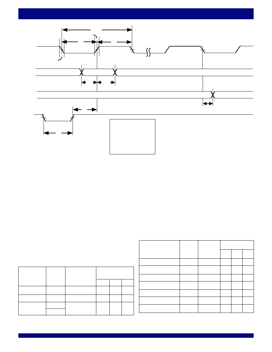
63
IDT72T51546/72T51556 2.5V, MULTI-QUEUE FLOW-CONTROL DEVICES
(32 QUEUES) 36 BIT WIDE CONFIGURATION 1,179,648 and 2,359,296 bits
COMMERCIAL AND INDUSTRIAL
TEMPERATURE RANGES
t
4
t
3
TDO
TDO
TDI/
TMS
TCK
TRST
t
DO
Notes to diagram:
t1 =
t
TCKLOW
t2 =
t
TCKHIGH
t3 =
t
TCKFALL
t4 = t
TCKRISE
t5 =
tRST
(reset pulse width)
t6 = tRSR (reset recovery)
5998 drw43
t
5
t
6
t
1
t
2
t
TCK
t
DH
t
DS
Figure 38. Standard JTAG Timing
SYSTEM INTERFACE PARAMETERS
Parameter
Symbol
Test
Conditions
Min.
Max. Units
JTAG Clock Input Period t
TCK
-
100
-
ns
JTAG Clock HIGH
t
TCKHIGH
-
40
-
ns
JTAG Clock Low
t
TCKLOW
-
40
-
ns
JTAG Clock Rise Time
t
TCKRISE
-
-
5
(1)
ns
JTAG Clock Fall Time
t
TCKFALL
-
-
5
(1)
ns
JTAG Reset
t
RST
-
50
-
ns
JTAG Reset Recovery
t
RSR
-
50
-
ns
JTAG AC ELECTRICAL
CHARACTERISTICS
(v
cc = 2.5V
Ī
5%; Tcase = 0įC to +85įC)
IDT72T51546
IDT72T51556
Parameter
Symbol
Test Conditions
Min.
Max.
Units
Data Output
t
DO
(1)
-
20
ns
Data Output Hold
t
DOH
(1)
0
-
ns
Data Input
t
DS
t
rise=3ns
10
-
ns
t
DH
t
fall=3ns
10
-
NOTE:
1. 50pf loading on external output signals.
NOTE:
1. Guaranteed by design.
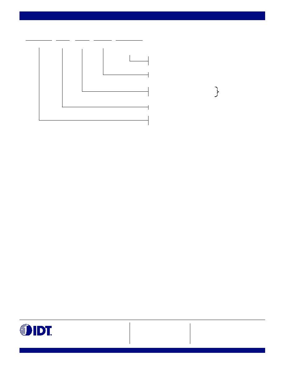
CORPORATE HEADQUARTERS
for SALES:
for Tech Support:
2975 Stender Way
800-345-7015 or 408-727-6116
408-330-1533
Santa Clara, CA 95054
fax: 408-492-8674
email: Flow-Controlhelp@idt.com
www.idt.com
64
Plastic Ball Grid Array (PBGA, BB256-1)
Commercial (0
įC to +70įC)
Industrial (-40
įC to +85įC)
Low Power
5998 drw44
Commercial Only
Commercial and Industrial
L
IDT
XXXXX
Device Type
X
Power
XX
Speed
X
Package
X
Process /
Temperature
Range
BLANK
I
(1)
72T51546
1,179,648 bits
2.5V Multi-Queue Flow-Control Device
72T51556
2,359,296 bits
2.5V Multi-Queue Flow-Control Device
Clock Cycle Time (t
CLK
)
Speed in Nanoseconds
BB
5
6
ORDERING INFORMATION
NOTE:
1. Industrial temperature range product for the 6ns is available as a standard device. All other speed grades available by special order.
DATASHEET DOCUMENT HISTORY
06/06/2003
pgs. 1 through 64.