 | –≠–ª–µ–∫—Ç—Ä–æ–Ω–Ω—ã–π –∫–æ–º–ø–æ–Ω–µ–Ω—Ç: 72V2105 | –°–∫–∞—á–∞—Ç—å:  PDF PDF  ZIP ZIP |
1
MARCH 2001
3.3 VOLT HIGH DENSITY CMOS
SUPERSYNC FIFOTM
131,072 x 18
262,144 x 18
IDT72V295
IDT72V2105
DSC-4668/2
2001 Integrated Device Technology, Inc.
The SuperSync FIFO is a trademark and the IDT logo is a registered trademark of Integrated Device Technology, Inc.
COMMERCIAL AND INDUSTRIAL TEMPERATURE RANGES
.EATURES:
∑
Choose among the following memory organizations:
IDT72V295
131,072 x 18
IDT72V2105
262,144 x 18
∑
Pin-compatible with the IDT72V255/72V265 and the IDT72V275/
72V285 SuperSync FIFOs
∑
10ns read/write cycle time (6.5ns access time)
∑
Fixed, low first word data latency time
∑
5V input tolerant
∑
Auto power down minimizes standby power consumption
∑
Master Reset clears entire FIFO
∑
Partial Reset clears data, but retains programmable settings
∑
Retransmit operation with fixed, low first word data latency time
∑
Empty, Full and Half-Full flags signal FIFO status
∑
Programmable Almost-Empty and Almost-Full flags, each flag can
default to one of two preselected offsets
∑
Program partial flags by either serial or parallel means
∑
Select IDT Standard timing (using
EF and FF flags) or First Word
Fall Through timing (using
OR and IR flags)
∑
Output enable puts data outputs into high impedance state
∑
Easily expandable in depth and width
∑
Independent Read and Write clocks (permit reading and writing
simultaneously)
∑
Available in the 64-pin Thin Quad Flat Pack (TQFP)
∑
High-performance submicron CMOS technology
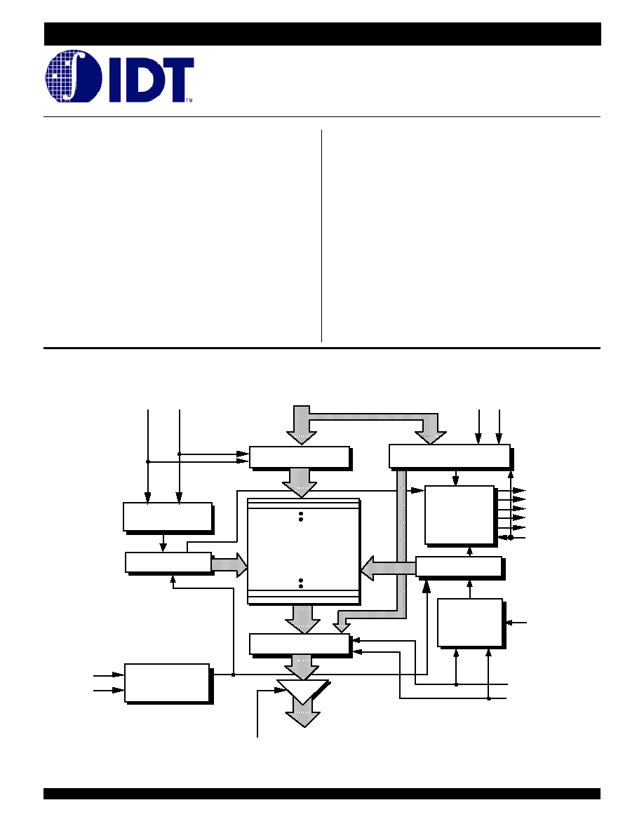
.UNCTIONAL BLOCK DIAGRAM
INPUT REGISTER
OUTPUT REGISTER
RAM ARRAY
131,072 x 18
262,144 x 18
FLAG
LOGIC
FF
/
IR
PAF
EF
/
OR
PAE
HF
READ POINTER
READ
CONTROL
LOGIC
WRITE CONTROL
LOGIC
WRITE POINTER
RESET
LOGIC
WEN
WCLK
D
0
-D
17
LD
MRS
REN
RCLK
OE
Q
0
-Q
17
OFFSET REGISTER
PRS
FWFT/SI
SEN
RT
4668 drw 01
DESCRIPTION:
The IDT72V295/72V2105 are exceptionally deep, high speed, CMOS
First-In-First-Out (FIFO) memories with clocked read and write controls. These
FIFOs offer numerous improvements over previous SuperSync FIFOs, includ-
ing the following:
∑ The limitation of the frequency of one clock input with respect to the other
has been removed. The Frequency Select pin (FS) has been removed,
2
COMMERCIAL AND INDUSTRIAL TEMPERATURE RANGES
IDT72V295/72V2105 3.3V HIGH DENSITY CMOS
SUPERSYNC FIFO
TM
131,072 x 18, 262,144 x 18
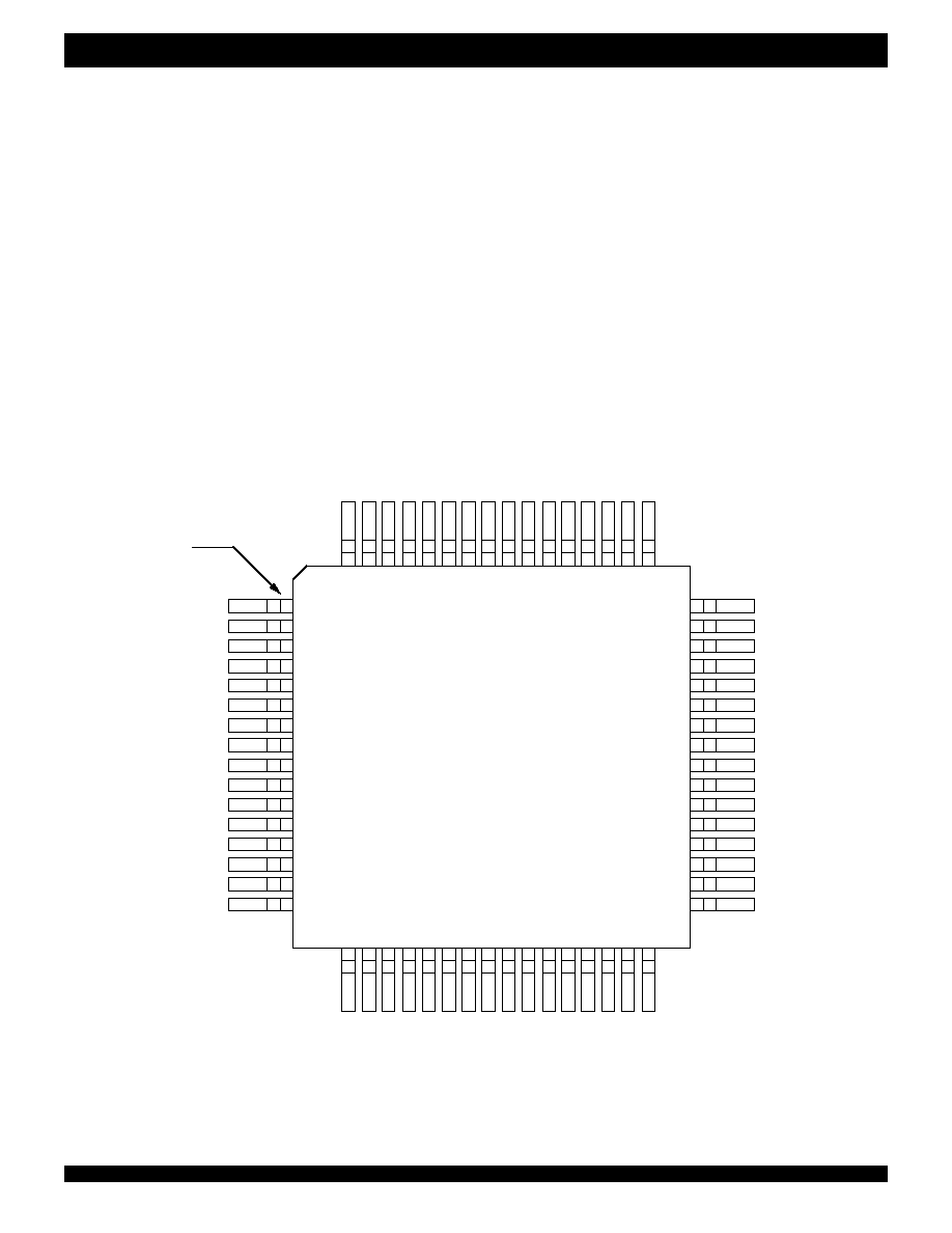
PIN CON.IGURATIONS
TQFP (PN64-1, order code: PF)
TOP VIEW
DESCRIPTION (CONTINUED)
thus it is no longer necessary to select which of the two clock inputs,
RCLK or WCLK, is running at the higher frequency.
∑ The period required by the retransmit operation is now fixed and short.
∑ The first word data latency period, from the time the first word is written
to an empty FIFO to the time it can be read, is now fixed and short. (The
variable clock cycle counting delay associated with the latency period
found on previous SuperSync devices has been eliminated on this
SuperSync family.)
SuperSync FIFOs are particularly appropriate for network, video, telecom-
munications, data communications and other applications that need to
buffer large amounts of data.
The input port is controlled by a Write Clock (WCLK) input and a Write
Enable (
WEN) input. Data is written into the FIFO on every rising edge of
WCLK when
WEN is asserted. The output port is controlled by a Read Clock
(RCLK) input and Read Enable (
REN) input. Data is read from the FIFO on
every rising edge of RCLK when
REN is asserted. An Output Enable (OE)
input is provided for three-state control of the outputs.
The frequencies of both the RCLK and the WCLK signals may vary from
0 to f
MAX
with complete independence. There are no restrictions on the
frequency of the one clock input with respect to the other.
There are two possible timing modes of operation with these devices:
IDT Standard mode and First Word Fall Through (FWFT) mode.
NOTE:
1. DC = Don't Care. Must be tied to GND or VCC, cannot be left open.
PIN 1
1
2
3
4
5
6
7
8
9
10
11
12
13
14
15
16
48
47
46
45
44
43
42
41
40
39
38
37
36
35
34
33
WEN
SEN
DC
(1)
V
CC
GND
D17
D16
D15
D14
D13
D12
D11
D10
D9
D8
D7
64 63 62 61 60 59 58 57 56 55 54 53 52 51 50 49
17 18 19 20 21 22 23 24 25 26 27 28 29 30 31 32
Q17
Q16
GND
Q15
Q14
V
CC
Q13
Q12
Q11
GND
Q10
Q9
Q8
Q7
Q6
GND
WCLK
PRS
MRS
LD
FWFT/SI
GND
FF
/
IR
PAF
HF
V
CC
PAE
EF
/
OR
RCLK
REN
RT
OE
Q5
Q4
V
CC
Q3
Q2
GND
Q1
Q0
GND
D0
D1
D2
D3
D4
D5
D6
4668 drw 02
3
COMMERCIAL AND INDUSTRIAL TEMPERATURE RANGES
IDT72V295/72V2105 3.3V HIGH DENSITY CMOS
SUPERSYNC FIFO
TM
131,072 x 18, 262,144 x 18
Figure 1. Block Diagram of Single 131,072 x 18 and 262,144 x 18 Synchronous FIFO
In IDT Standard mode, the first word written to an empty FIFO will not
appear on the data output lines unless a specific read operation is
performed. A read operation, which consists of activating
REN and enabling
a rising RCLK edge, will shift the word from internal memory to the data
output lines.
In FWFT mode, the first word written to an empty FIFO is clocked directly
to the data output lines after three transitions of the RCLK signal. A
REN
does not have to be asserted for accessing the first word. However,
subsequent words written to the FIFO do require a LOW on
REN for access.
The state of the FWFT/SI input during Master Reset determines the timing
mode in use.
For applications requiring more data storage capacity than a single FIFO
can provide, the FWFT timing mode permits depth expansion by chaining
FIFOs in series (i.e. the data outputs of one FIFO are connected to the
corresponding data inputs of the next). No external logic is required.
These FIFOs have five flag pins,
EF/OR (Empty Flag or Output Ready),
FF/IR (Full Flag or Input Ready), HF (Half-full Flag), PAE (Programmable
Almost-Empty flag) and
PAF (Programmable Almost-Full flag). The EF and
FF functions are selected in IDT Standard mode. The IR and OR functions
are selected in FWFT mode.
HF, PAE and PAF are always available for use,
irrespective of timing mode.
PAE and PAF can be programmed independently to switch at any point
in memory. (See Table I and Table II.) Programmable offsets determine
the flag switching threshold and can be loaded by two methods: parallel or
serial. Two default offset settings are also provided, so that
PAE can be set
to switch at 127 or 1,023 locations from the empty boundary and the
PAF
threshold can be set at 127 or 1,023 locations from the full boundary. These
choices are made with the
LD pin during Master Reset
.
DATA OUT (Q
0
- Q
n
)
DATA IN (D
0
- D
n
)
MASTER RESET (
MRS
)
READ CLOCK (RCLK)
READ ENABLE (
REN
)
OUTPUT ENABLE (
OE
)
EMPTY FLAG/OUTPUT READY (
EF
/
OR
)
PROGRAMMABLE ALMOST-EMPTY (
PAE
)
WRITE CLOCK (WCLK)
WRITE ENABLE (
WEN
)
LOAD (
LD
)
FULL FLAG/INPUT READY (
FF
/
IR
)
PROGRAMMABLE ALMOST-FULL (
PAF
)
IDT
72V295
72V2105
PARTIAL RESET (
PRS
)
FIRST WORD FALL THROUGH/SERIAL INPUT
(FWFT/SI)
RETRANSMIT (
RT
)
4668 drw 03
HALF FULL FLAG (
HF
)
SERIAL ENABLE(
SEN
)
For serial programming,
SEN together with LD on each rising edge of
WCLK, are used to load the offset registers via the Serial Input (SI). For
parallel programming,
WEN together with LD on each rising edge of WCLK,
are used to load the offset registers via D
n
.
REN together with LD on each
rising edge of RCLK can be used to read the offsets in parallel from Q
n
regardless of whether serial or parallel offset loading has been selected.
During Master Reset (
MRS) the following events occur: The read and
write pointers are set to the first location of the FIFO. The FWFT pin selects
IDT Standard mode or FWFT mode. The
LD pin selects either a partial flag
default setting of 127 with parallel programming or a partial flag default
setting of 1,023 with serial programming. The flags are updated according
to the timing mode and default offsets selected.
The Partial Reset (
PRS) also sets the read and write pointers to the first
location of the memory. However, the timing mode, partial flag program-
ming method, and default or programmed offset settings existing before
Partial Reset remain unchanged. The flags are updated according to the
timing mode and offsets in effect.
PRS is useful for resetting a device in mid-
operation, when reprogramming partial flags would be undesirable.
The Retransmit function allows data to be reread from the FIFO. A LOW
on the
RT input during a rising RCLK edge initiates a retransmit operation
by setting the read pointer to the first location of the memory array.
If, at any time, the FIFO is not actively performing an operation, the chip
will automatically power down. Once in the power down state, the standby
supply current consumption is minimized. Initiating any operation (by
activating control inputs) will immediately take the device out of the power
down state.
The IDT72V295/72V2105 are fabricated using IDT's high speed submi-
cron CMOS technology.

4
COMMERCIAL AND INDUSTRIAL TEMPERATURE RANGES
IDT72V295/72V2105 3.3V HIGH DENSITY CMOS
SUPERSYNC FIFO
TM
131,072 x 18, 262,144 x 18
PIN DESCRIPTION
Symbol
Name
I/O
Description
D
0
≠D
17
Data Inputs
I
Data inputs for a 18-bit bus.
MRS
Master Reset
I
MRS initializes the read and write pointers to zero and sets the output register to
all zeroes. During Master Reset, the FIFO is configured for either FWFT or IDT
Standard mode, one of two programmable flag default settings, and serial or
parallel programming of the offset settings.
PRS
Partial Reset
I
PRS initializes the read and write pointers to zero and sets the output register to
all zeroes. During Partial Reset, the existing mode (IDT or FWFT), programming
method (serial or parallel), and programmable flag settings are all retained.
RT
Retransmit
I
RT asserted on the rising edge of RCLK initializes the READ pointer to zero, sets
the
EF flag to LOW (OR to HIGH in FWFT mode) temporarily and does not disturb
the write pointer, programming method, existing timing mode or programmable flag
settings.
RT is useful to reread data from the first physical location of the FIFO.
FWFT/SI
First Word Fall
I
During Master Reset, selects First Word Fall Through or IDT Standard mode.
Through/Serial In
After Master Reset, this pin functions as a serial input for loading offset registers
WCLK
Write Clock
I
When enabled by
WEN, the rising edge of WCLK writes data into the FIFO and
offsets into the programmable registers for parallel programming, and when
enabled by
SEN, the rising edge of WCLK writes one bit of data into the
programmable register for serial programming.
WEN
Write Enable
I
WEN enables WCLK for writing data into the FIFO memory and offset registers.
RCLK
Read Clock
I
When enabled by
REN, the rising edge of RCLK reads data from the FIFO
memory and offsets from the programmable registers.
REN
Read Enable
I
REN enables RCLK for reading data from the FIFO memory and offset registers.
OE
Output Enable
I
OE controls the output impedance of Q
n.
SEN
Serial Enable
I
SEN enables serial loading of programmable flag offsets.
LD
Load
I
During Master Reset,
LD selects one of two partial flag default offsets (127 or
1,023) and determines the flag offset programming method, serial or parallel. After
Master Reset, this pin enables writing to and reading from the offset registers.
DC
Don't Care
I
This pin must be tied to either V
CC
or GND and must not toggle after Master
Reset.
FF/IR
Full Flag/
O
In the IDT Standard mode, the
FF function is selected. FF indicates whether or
Input Ready
not the FIFO memory is full. In the FWFT mode, the
IR function is selected. IR
indicates whether or not there is space available for writing to the FIFO memory.
EF/OR
Empty Flag/
O
In the IDT Standard mode, the
EF function is selected. EF indicates whether or
Output Ready
not the FIFO memory is empty. In FWFT mode, the
OR function is selected.
OR indicates whether or not there is valid data available at the outputs.
PAF
Programmable
O
PAF goes LOW if the number of words in the FIFO memory is more than
Almost-Full Flag
total word capacity of the FIFO minus the full offset value m, which is stored in the
Full Offset register. There are two possible default values for m: 127 or 1,023.
PAE
Programmable
O
PAE goes LOW if the number of words in the FIFO memory is less than offset n,
Almost-Empty Flag
which is stored in the Empty Offset register. There are two possible default values
for n: 127 or 1,023. Other values for n can be programmed into the device.
HF
Half-Full Flag
O
HF indicates whether the FIFO memory is more or less than half-full.
Q
0
≠Q
17
Data Outputs
O
Data outputs for an 18-bit bus.
V
CC
Power
+3.3 Volt power supply pins.
GND
Ground
Ground pins.
5
COMMERCIAL AND INDUSTRIAL TEMPERATURE RANGES
IDT72V295/72V2105 3.3V HIGH DENSITY CMOS
SUPERSYNC FIFO
TM
131,072 x 18, 262,144 x 18
NOTES:
1. With output deselected, (
OE
V
IH
).
2. Characterized values, not currently tested.
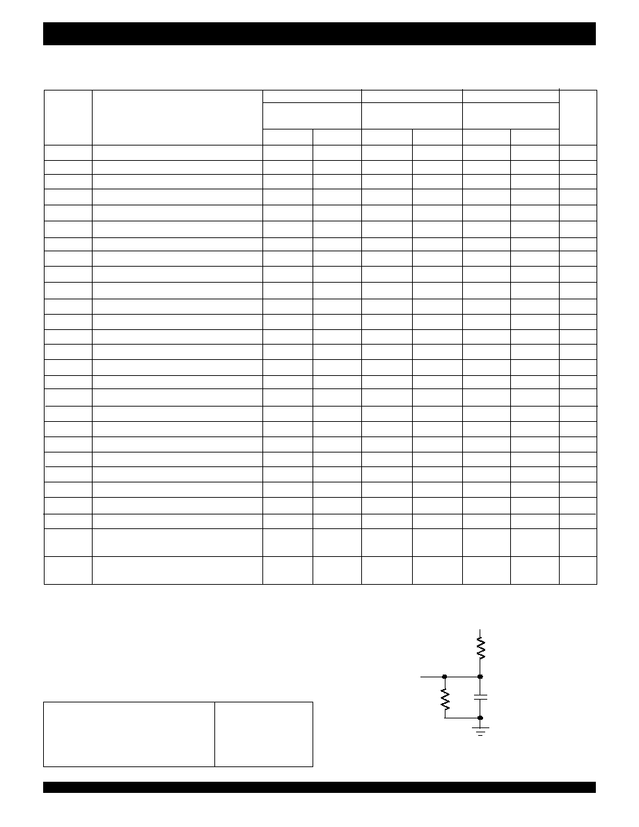
DC ELECTRICAL CHARACTERISTICS
(Commercial: V
CC
= 3.3V ± 0.15V, T
A
= 0
∞
C to +70
∞
C; Industrial: V
CC
= 3.3V ± 0.15V, T
A
= -40
∞
C to +85
∞
C)
CAPACITANCE
(T
A
= +25
∞
C, f = 1.0MHz)
Symbol
Parameter
(1)
Conditions
Max.
Unit
C
IN
(2)
Input
V
IN
= 0V
10
pF
Capacitance
C
OUT
(1,2)
Output
V
OUT
= 0V
10
pF
Capacitance
IDT72V295L
IDT72V2105L
Commercial and Industrial
(1)
t
CLK
= 10, 15, 20 ns
Symbol
Parameter
Min.
Max.
Unit
I
LI
(2)
Input Leakage Current
≠1
1
µ A
I
LO
(3)
Output Leakage Current
≠10
10
µA
V
OH
Output Logic "1" Voltage, I
OH
= ≠2 mA
2.4
--
V
V
OL
Output Logic "0" Voltage, I
OL
= 8 mA
--
0.4
V
I
CC1
(4,5,6)
Active Power Supply Current
--
60
mA
I
CC2
(4,7)
Standby Current
--
20
mA
NOTES
:
1. Industrial temperature range product for the 15ns speed grade is available as a standard device.
2. Measurements with 0.4
V
IN
V
CC
.
3.
OE
V
IH,
0.4
V
OUT
-
V
CC.
4. Tested with outputs open (I
OUT
= 0).
5. RCLK and WCLK toggle at 20 MHz and data inputs switch at 10 MHz.
6. Typical I
CC1
= 5 + f
S
+ 0.02*C
L
*f
S
(in mA) with V
CC
= 3.3V, t
A
= 25
∞
C, f
S
= WCLK frequency = RCLK frequency (in MHz, using TTL levels), data switching at f
S
/2,
C
L
= capacitive load (in pF).
7. All Inputs = V
CC
- 0.2V or GND + 0.2V, except RCLK and WCLK, which toggle at 20 MHz.
ABSOLUTE MAXIMUM RATINGS
Symbol
Rating
Com'l & Ind'l
Unit
V
TERM
(2)
Terminal Voltage
≠0.5 to +4.5
V
with respect to GND
T
STG
Storage
≠55 to +125
∞
C
Temperature
I
OUT
DC Output Current
≠50 to +50
mA
RECOMMENDED DC OPERATING
CONDITIONS
NOTE:
1. 1.5V undershoots are allowed for 10ns once per cycle.
Symbol
Parameter
Min.
Typ.
Max.
Unit
V
CC
Supply Voltage (Com'l & Ind'l)
3.0
3.3
3.6
V
GND
Supply Voltage (Com'l & Ind'l)
0
0
0
V
V
IH
Input High Voltage (Com'l & Ind'l)
2.0
--
5.5
V
V
IL
(1)
Input Low Voltage (Com'l & Ind'l)
--
--
0.8
V
T
A
Operating Temperature Commercial
0
--
+70
∞
C
T
A
Operating Temperature Industrial
-40
--
+85
∞
C
NOTES:
1. Stresses greater than those listed under ABSOLUTE MAXIMUM RATINGS may cause
permanent damage to the device. This is a stress rating only and functional operation
of the device at these or any other conditions above those indicated in the operational
sections of this specification is not implied. Exposure to absolute maximum rating
conditions for extended periods may affect reliability.
2. V
CC
terminal only.
6
COMMERCIAL AND INDUSTRIAL TEMPERATURE RANGES
IDT72V295/72V2105 3.3V HIGH DENSITY CMOS
SUPERSYNC FIFO
TM
131,072 x 18, 262,144 x 18
AC ELECTRICAL CHARACTERISTICS
(1)
(Commercial: V
CC
= 3.3V ± 0.3V, T
A
= 0
∞
C to +70
∞
C; Industrial: V
CC
= 3.3V ± 0.15V, T
A
= -40
∞
C to +85
∞
C)
Commercial
Com'l & Ind'l
Commercial
IDT72V295L10
IDT72V295L15
IDT72V295L20
IDT72V2105L10
IDT72V2105L15
IDT72V2105L20
Symbol
Parameter
Min.
Max.
Min.
Max.
Min.
Max.
Unit
f
S
Clock Cycle Frequency
--
100
--
66.7
--
50
MHz
t
A
Data Access Time
2
6.5
2
10
2
12
ns
t
CLK
Clock Cycle Time
10
--
15
--
20
--
ns
t
CLKH
Clock High Time
4.5
--
6
--
8
--
ns
t
CLKL
Clock Low Time
4.5
--
6
--
8
--
ns
t
DS
Data Setup Time
3
--
4
--
5
--
ns
t
DH
Data Hold Time
0.5
--
1
--
1
--
ns
t
ENS
Enable Setup Time
3
--
4
--
5
--
ns
t
ENH
Enable Hold Time
0.5
--
1
--
1
--
ns
t
LDS
Load Setup Time
3
--
4
--
5
--
ns
t
LDH
Load Hold Time
0.5
--
1
--
1
--
ns
t
RS
Reset Pulse Width
(3)
10
--
15
--
20
--
ns
t
RSS
Reset Setup Time
15
--
15
--
20
--
ns
t
RSR
Reset Recovery Time
10
--
15
--
20
--
ns
t
RSF
Reset to Flag and Output Time
--
10
--
15
--
20
ns
t
FWFT
Mode Select Time
0
--
0
--
0
--
ns
t
RTS
Retransmit Setup Time
3
--
4
--
5
--
ns
t
OLZ
Output Enable to Output in Low Z
(4)
0
--
0
--
0
--
ns
t
OE
Output Enable to Output Valid
2
6
2
8
2
10
ns
t
OHZ
Output Enable to Output in High Z
(4)
2
6
2
8
2
10
ns
t
WFF
Write Clock to
FF or IR
--
6.5
--
10
--
12
ns
t
REF
Read Clock to
EF or OR
--
6.5
--
10
--
12
ns
t
PAF
Write Clock to
PAF
--
6.5
--
10
--
12
ns
t
PAE
Read Clock to
PAE
--
6.5
--
10
--
12
ns
t
HF
Clock to
HF
--
16
--
20
--
22
ns
t
SKEW1
Skew time between RCLK and WCLK
8
--
9
--
10
--
ns
for
EF/OR and FF/IR
t
SKEW2
Skew time between RCLK and WCLK
12
--
14
--
15
--
ns
for
PAE and PAF
NOTES:
1. Industrial temperature range product for the 15ns speed grade is available as a standard device.
2. All AC timings apply to both Standard IDT mode and First Word Fall Through mode.
3. Pulse widths less than minimum values are not allowed.
4. Values guaranteed by design, not currently tested.
Input Pulse Levels
GND to 3.0V
Input Rise/Fall Times
3ns
Input Timing Reference Levels
1.5V
Output Reference Levels
1.5V
Output Load
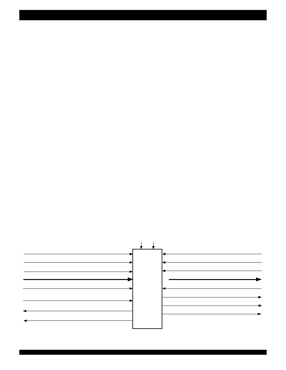
See Figure 2
AC TEST CONDITIONS
Figure 2. Output Load
* Includes jig and scope capacitances.
4668 drw 04
330
30pF*
510
3.3V
D.U.T.

7
COMMERCIAL AND INDUSTRIAL TEMPERATURE RANGES
IDT72V295/72V2105 3.3V HIGH DENSITY CMOS
SUPERSYNC FIFO
TM
131,072 x 18, 262,144 x 18
If the FIFO is full, the first read operation will cause
FF to go HIGH.
Subsequent read operations will cause
PAF and HF to go HIGH at the
conditions described in Table 1. If further read operations occur, without
write operations,
PAE will go LOW when there are n words in the FIFO,
where n is the empty offset value. Continuing read operations will cause the
FIFO to become empty. When the last word has been read from the FIFO,
the
EF will go LOW inhibiting further read operations. REN is ignored when
the FIFO is empty.
When configured in IDT Standard mode, the
EF and FF outputs are
double register-buffered outputs.
Relevant timing diagrams for IDT Standard mode can be found in Figure
7, 8 and 11.
FIRST WORD FALL THROUGH MODE (FWFT)
In this mode, the status flags,
IR, PAF, HF, PAE, and OR operate in the
manner outlined in Table 2. To write data into to the FIFO,
WEN must be
LOW. Data presented to the DATA IN lines will be clocked into the FIFO on
subsequent transitions of WCLK. After the first write is performed, the
Output Ready (
OR) flag will go LOW. Subsequent writes will continue to fill
up the FIFO.
PAE will go HIGH after n + 2 words have been loaded into the
FIFO, where n is the empty offset value. The default setting for this value
is stated in the footnote of Table 2. This parameter is also user program-
mable. See section on Programmable Flag Offset Loading.
If one continued to write data into the FIFO, and we assumed no read
operations were taking place, the
HF would toggle to LOW once the
65,538th word for the IDT72V295 and 131,074th word for the IDT72V2105,
respectively was written into the FIFO. Continuing to write data into the
FIFO will cause the
PAF to go LOW. Again, if no reads are performed, the
PAF will go LOW after (131,073-m) writes for the IDT72V295 and (262,145-
m) writes for the IDT72V2105, where m is the full offset value. The default
setting for this value is stated in the footnote of Table 2.
When the FIFO is full, the Input Ready (
IR) flag will go HIGH, inhibiting
further write operations. If no reads are performed after a reset,
IR will go
HIGH after D writes to the FIFO. D = 131,073 writes for the IDT72V295 and
262,145 writes for the IDT72V2105, respectively. Note that the additional
word in FWFT mode is due to the capacity of the memory plus output
register.
If the FIFO is full, the first read operation will cause the
IR flag to go LOW.
Subsequent read operations will cause the
PAF and HF to go HIGH at the
conditions described in Table 2. If further read operations occur, without
write operations, the
PAE will go LOW when there are n + 1 words in the
FIFO, where n is the empty offset value. Continuing read operations will
cause the FIFO to become empty. When the last word has been read from
the FIFO,
OR will go HIGH inhibiting further read operations. REN is ignored
when the FIFO is empty.
When configured in FWFT mode, the
OR flag output is triple register-
buffered, and the
IR flag output is double register-buffered.
Relevant timing diagrams for FWFT mode can be found in Figure 9, 10
and 12.
.UNCTIONAL DESCRIPTION
TIMING MODES: IDT STANDARD vs FIRST WORD FALL THROUGH
(FWFT) MODE
The IDT72V295/72V2105 support two different timing modes of opera-
tion: IDT Standard mode or First Word Fall Through (FWFT) mode. The
selection of which mode will operate is determined during Master Reset, by
the state of the FWFT/SI input.
If, at the time of Master Reset, FWFT/SI is LOW, then IDT Standard
mode will be selected. This mode uses the Empty Flag (
EF) to indicate
whether or not there are any words present in the FIFO. It also uses the Full
Flag function (
FF) to indicate whether or not the FIFO has any free space
for writing. In IDT Standard mode, every word read from the FIFO, including
the first, must be requested using the Read Enable (
REN) and RCLK.
If, at the time of Master Reset, FWFT/SI is HIGH, then FWFT mode will
be selected. This mode uses Output Ready (
OR) to indicate whether or not
there is valid data at the data outputs (Q
n)
. It also uses Input Ready (
IR) to
indicate whether or not the FIFO has any free space for writing. In the FWFT
mode, the first word written to an empty FIFO goes directly to Q
n
after three
RCLK rising edges,
REN = LOW is not necessary. Subsequent words must
be accessed using the Read Enable (
REN) and RCLK.
Various signals, both input and output signals operate differently de-
pending on which timing mode is in effect.
IDT STANDARD MODE
In this mode, the status flags,
FF, PAF, HF, PAE, and EF operate in the
manner outlined in Table 1. To write data into to the FIFO, Write Enable (
WEN)
must be LOW. Data presented to the DATA IN lines will be clocked into the FIFO
on subsequent transitions of the Write Clock (WCLK). After the first write is
performed, the Empty Flag (
EF) will go HIGH. Subsequent writes will continue
to fill up the FIFO. The Programmable Almost-Empty flag (
PAE) will go HIGH
after n + 1 words have been loaded into the FIFO, where n is the empty offset
value. The default setting for this value is stated in the footnote of Table 1. This
parameter is also user programmable. See section on Programmable Flag
Offset Loading.
If one continued to write data into the FIFO, and we assumed no read
operations were taking place, the Half-Full flag (
HF) would toggle to LOW
once the 65,537th word for IDT72V295 and 131,073rd word for IDT72V2105
respectively was written into the FIFO. Continuing to write data into the
FIFO will cause the Programmable Almost-Full flag (
PAF) to go LOW. Again,
if no reads are performed, the
PAF will go LOW after (131,072-m) writes for
the IDT72V295 and (262,144-m) writes for the IDT72V2105. The offset "m"
is the full offset value. The default setting for this value is stated in the
footnote of Table 1. This parameter is also user programmable. See section
on Programmable Flag Offset Loading.
When the FIFO is full, the Full Flag (
FF) will go LOW, inhibiting further
write operations. If no reads are performed after a reset,
FF will go LOW
after D writes to the FIFO. D = 131,072 writes for the IDT72V295 and
262,144 for the IDT72V2105, respectively.
8
COMMERCIAL AND INDUSTRIAL TEMPERATURE RANGES
IDT72V295/72V2105 3.3V HIGH DENSITY CMOS
SUPERSYNC FIFO
TM
131,072 x 18, 262,144 x 18
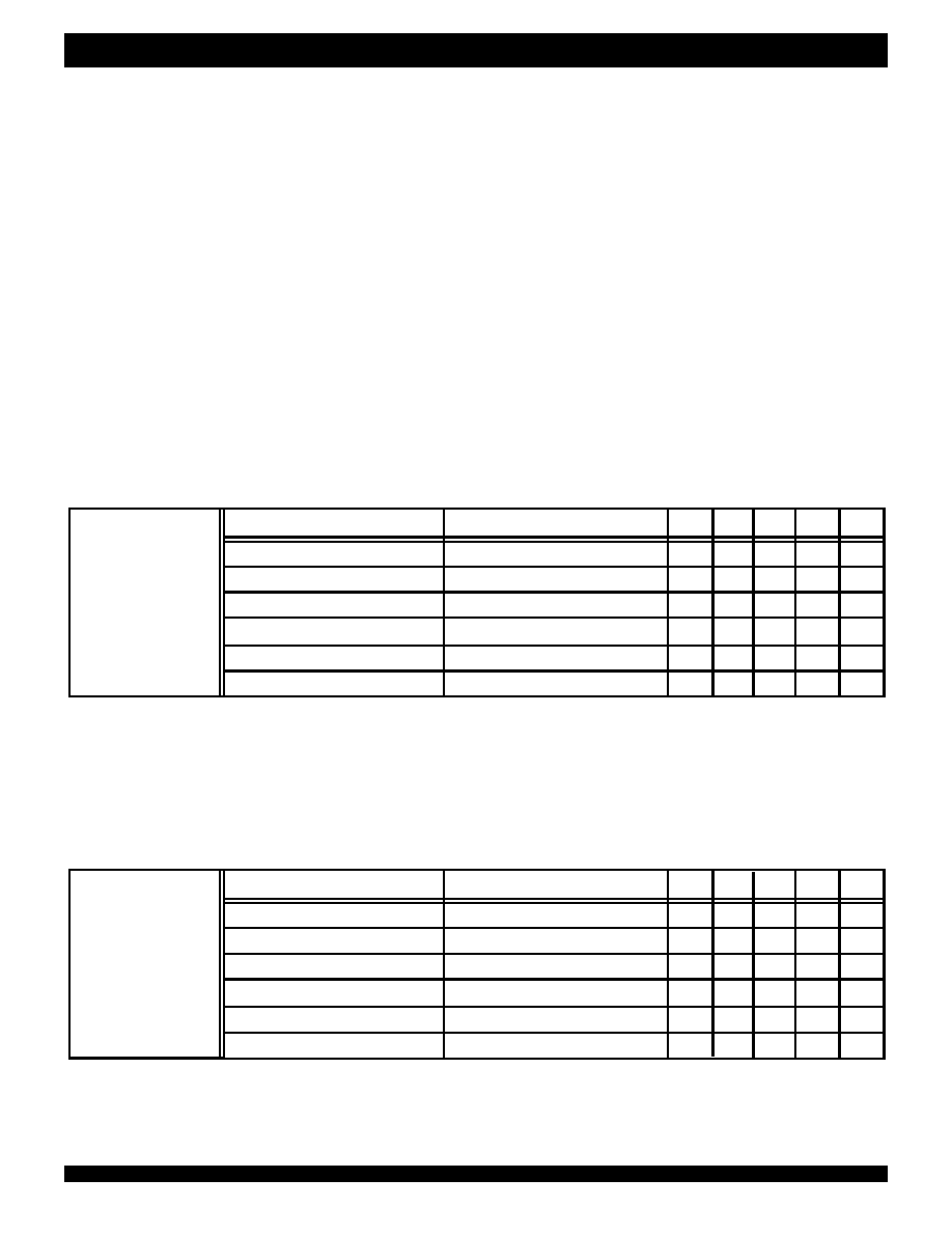
Number of
Words in
FIFO
0
1 to n
(1)
(n+1) to 65,536
65,537 to (131,072-(m+1))
(131,072-m)
(2)
to 131,071
131,072
0
1 to n
(1)
(n+1) to 131,072
131,073 to (262,144-(m+1))
(262,144-m)
(2)
to 262,143
262,144
TABLE II
STATUS FLAGS FOR FWFT MODE
IDT72V295
IDT72V2105
FF PAF HF PAE EF
H
H
H
L
L
H
H
H
L
H
H
H
H
H
H
H
H
L
H
H
H
L
L
H
H
L
L
L
H
H
TABLE I
STATUS FLAGS FOR IDT STANDARD MODE
4668 drw 05
0
1 to n+1
(1)
(n+2) to 65,537
(131,073-m)
(2)
to 131,072
131,073
0
1 to n+1
(1)
(n+2) to 131,073
131,074 to (262,145-(m+1))
(262,145-m)
(2)
to 262,144
262,145
IR PAF HF PAE OR
L
H
H
L
H
L
H
H
L
L
L
H
H
H
L
L
H
L
H
L
L
L
L
H
L
H
L
L
H
L
IDT72V295
IDT72V2105
Number of
Words in
FIFO
(
1)
65,538 to (131,073-(m+1))
NOTES:
1. n = Empty Offset, Default Values: n = 127 when parallel offset loading is selected or n = 1,023 when serial offset loading is selected.
2. m = Full Offset, Default Values: m = 127 when parallel offset loading is selected or m = 1,023 when serial offset loading is selected.
NOTES:
1. n = Empty Offset, Default Values: n = 127 when parallel offset loading is selected or n = 1,023 when serial offset loading is selected.
2. m = Full Offset, Default Values: m = 127 when parallel offset loading is selected or m = 1,023 when serial offset loading is selected.
PROGRAMMING FLAG OFFSETS
Full and Empty Flag offset values are user programmable. The
IDT72V295/72V2105 has internal registers for these offsets. Default set-
tings are stated in the footnotes of Table 1 and Table 2. Offset values can
be programmed into the FIFO in one of two ways; serial or parallel loading
method. The selection of the loading method is done using the
LD (Load)
pin. During Master Reset, the state of the
LD input determines whether serial
or parallel flag offset programming is enabled. A HIGH on
LD during Master
Reset selects serial loading of offset values and in addition, sets a default
PAE offset value of 3FFH (a threshold 1,023 words from the empty
boundary), and a default
PAF offset value of 3FFH (a threshold 1,023 words
from the full boundary). A LOW on
LD during Master Reset selects parallel
loading of offset values, and in addition, sets a default
PAE offset value of
07FH (a threshold 127 words from the empty boundary), and a default
PAF
offset value of 07FH (a threshold 127 words from the full boundary). See
Figure 3, Offset Register Location and Default Values.
In addition to loading offset values into the FIFO, it also possible to read
the current offset values. It is only possible to read offset values via parallel
read.
Figure 4, Programmable Flag Offset Programming Sequence, summa-
rizes the control pins and sequence for both serial and parallel programming
modes. For a more detailed description, see discussion that follows.
The offset registers may be programmed (and reprogrammed) any time
after Master Reset, regardless of whether serial or parallel programming
has been selected.
9
COMMERCIAL AND INDUSTRIAL TEMPERATURE RANGES
IDT72V295/72V2105 3.3V HIGH DENSITY CMOS
SUPERSYNC FIFO
TM
131,072 x 18, 262,144 x 18
Figure 4. Programmable Flag Offset Programming Sequence
Figure 3. Offset Register Location and Default Values
17
0
007FH if
LD
is LOW at Master Reset,
03FFH if
LD
is HIGH at Master Reset
DEFAULT VALUE
FULL OFFSET (LSB) REGISTER
17
0
DEFAULT VALUE
007FH if
LD
is LOW at Master Reset,
03FFH if
LD
is HIGH at Master Reset
15
IDT72V295 (131,072 x 18-BIT)
16
15
16
EMPTY OFFSET (LSB) REGISTER
17
0
007FH if
LD
is LOW at Master Reset,
03FFH if
LD
is HIGH at Master Reset
FULL OFFSET (LSB) REGISTER
17
0
DEFAULT VALUE
DEFAULT VALUE
007FH if
LD
is LOW at Master Reset,
03FFH if
LD
is HIGH at Master Reset
15
IDT72V2105 (262,144 x 18-BIT)
16
15
16
EMPTY OFFSET (LSB) REGISTER
17
DEFAULT
0H
0
1
17
0
2 1
17
0
2 1
17
0
1
EMPTY OFFSET
(MSB) REGISTER
DEFAULT
0H
FULL OFFSET
(MSB) REGISTER
DEFAULT
0H
EMPTY OFFSET
(MSB) REGISTER
DEFAULT
0H
FULL OFFSET
(MSB) REGISTER
4668 drw 06
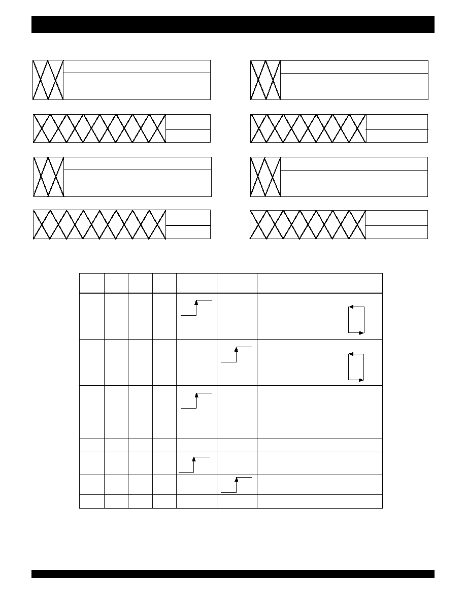
WCLK
RCLK
X
X
X
X
X
X
X
X
4668 drw 07
LD
0
0
X
1
1
1
0
WEN
0
1
1
0
X
1
1
REN
1
0
1
X
0
1
1
X
SEN
1
1
1
X
X
X
0
No Operation
Write Memory
Read Memory
No Operation
Parallel write to registers:
Empty Offset (LSB)
Empty Offset (MSB)
Full Offset (LSB)
Full Offset (MSB)
Serial shift into registers:
34 bits for the 72V295
36 bits for the 72V2105
1 bit for each rising WCLK edge
Starting with Empty Offset (LSB)
Ending with Full Offset (MSB)
IDT72V295
IDT72V2105
Parallel read from registers:
Empty Offset (LSB)
Empty Offset (MSB)
Full Offset (LSB)
Full Offset (MSB)
NOTES:
1. The programming method can only be selected at Master Reset.
2. Parallel reading of the offset registers is always permitted regardless of which programming method has been selected.
3. The programming sequence applies to both IDT Standard and FWFT modes.

10
COMMERCIAL AND INDUSTRIAL TEMPERATURE RANGES
IDT72V295/72V2105 3.3V HIGH DENSITY CMOS
SUPERSYNC FIFO
TM
131,072 x 18, 262,144 x 18
SERIAL PROGRAMMING MODE
If Serial Programming mode has been selected, as described above, then
programming of
PAE and PAF values can be achieved by using a combina-
tion of the
LD, SEN, WCLK and SI input pins. Programming PAE and PAF
proceeds as follows: when
LD and SEN are set LOW, data on the SI input
are written, one bit for each WCLK rising edge, starting with the Empty
Offset LSB and ending with the Full Offset MSB. A total of 34 bits for the
IDT72V295 and 36 bits for the IDT72V2105. See Figure 13, Serial Loading
of Programmable Flag Registers, for the timing diagram for this mode.
Using the serial method, individual registers cannot be programmed
selectively.
PAE and PAF can show a valid status only after the complete
set of bits (for all offset registers) has been entered. The registers can be
reprogrammed as long as the complete set of new offset bits is entered.
When
LD is LOW and SEN is HIGH, no serial write to the registers can occur.
Write operations to the FIFO are allowed before and during the serial
programming sequence. In this case, the programming of all offset bits
does not have to occur at once. A select number of bits can be written to
the SI input and then, by bringing
LD and SEN HIGH, data can be written to
FIFO memory via D
n
by toggling
WEN. When WEN is brought HIGH with LD
and
SEN restored to a LOW, the next offset bit in sequence is written to the
registers via SI. If an interruption of serial programming is desired, it is
sufficient either to set
LD LOW and deactivate SEN or to set SEN LOW and
deactivate
LD. Once LD and SEN are both restored to a LOW level, serial
offset programming continues.
From the time serial programming has begun, neither partial flag will be
valid until the full set of bits required to fill all the offset registers has been
written. Measuring from the rising WCLK edge that achieves the above
criteria;
PAF will be valid after two more rising WCLK edges plus t
PAF
,
PAE
will be valid after the next two rising RCLK edges plus t
PAE
plus t
SKEW2
.
It is not possible to read the flag offset values in a serial mode.
PARALLEL MODE
If Parallel Programming mode has been selected, as described above,
then programming of
PAE and PAF values can be achieved by using a
combination of the
LD, WCLK , WEN and D
n
input pins. For the ID72V295/
72V2105, programming
PAE and PAF proceeds as follows: when LD and
WEN are set LOW, data on the inputs Dn are written into the Empty Offset
LSB Register on the first LOW-to-HIGH transition of WCLK. Upon the
second LOW-to-HIGH transition of WCLK, data are written into the Empty
Offset MSB Register. Upon the third LOW-to-HIGH transition of WCLK,
data are written into the Full Offset LSB Register. Upon the fourth LOW-to-
HIGH transition of WCLK, data are written into the Full Offset MSB Register.
The fifth transition of WCLK writes, once again, to the Empty Offset LSB
Register. See Figure 14, Parallel Loading of Programmable Flag Registers, for
the timing diagram for this mode.
The act of writing offsets in parallel employs a dedicated write offset
register pointer. The act of reading offsets employs a dedicated read offset
register pointer. The two pointers operate independently; however, a read
and a write should not be performed simultaneously to the offset registers.
A Master Reset initializes both pointers to the Empty Offset (LSB) register.
A Partial Reset has no effect on the position of these pointers.
Write operations to the FIFO are allowed before and during the parallel
programming sequence. In this case, the programming of all offset registers
does not have to occur at one time. One, two or more offset registers can
be written and then by bringing
LD HIGH, write operations can be redirected
to the FIFO memory. When
LD is set LOW again, and WEN is LOW, the next
offset register in sequence is written to. As an alternative to holding
WEN
LOW and toggling
LD, parallel programming can also be interrupted by
setting
LD LOW and toggling WEN.
Note that the status of a partial flag (
PAE or PAF) output is invalid during
the programming process. From the time parallel programming has begun,
a partial flag output will not be valid until the appropriate offset word has
been written to the register(s) pertaining to that flag. Measuring from the
rising WCLK edge that achieves the above criteria;
PAF will be valid after two
more rising WCLK edges plus t
PAF
,
PAE will be valid after the next two rising
RCLK edges plus t
PAE
plus t
SKEW2
.
The act of reading the offset registers employs a dedicated read offset
register pointer. The contents of the offset registers can be read on the Q
0
-
Q
n
pins when
LD is set LOW and REN is set LOW. For the IDT72V295/
72V2105, data are read via Q
n
from the Empty Offset LSB Register on the
first LOW-to-HIGH transition of RCLK. Upon the second LOW-to-HIGH
transition of RCLK, data are read from the Empty Offset MSB Register.
Upon the third LOW-to-HIGH transition of RCLK, data are read from the Full
Offset LSB Register. Upon the fourth LOW-to-HIGH transition of RCLK,
data are read from the Full Offset MSB Register. The fifth transition of RCLK
reads, once again, from the Empty Offset LSB Register. See Figure 15,
Parallel Read of Programmable Flag Registers, for the timing diagram for
this mode.
It is permissible to interrupt the offset register read sequence with reads
or writes to the FIFO. The interruption is accomplished by deasserting
REN,
LD, or both together. When REN and LD are restored to a LOW level, reading
of the offset registers continues where it left off. It should be noted, and care
should be taken from the fact that when a parallel read of the flag offsets is
performed, the data word that was present on the output lines Qn will be
overwritten.
Parallel reading of the offset registers is always permitted regardless of
which timing mode (IDT Standard or FWFT modes) has been selected.
RETRANSMIT OPERATION
The Retransmit operation allows data that has already been read to be
accessed again. There are two stages: first, a setup procedure that resets
the read pointer to the first location of memory, then the actual retransmit,
which consists of reading out the memory contents, starting at the beginning
of memory.
Retransmit setup is initiated by holding
RT LOW during a rising RCLK
edge.
REN and WEN must be HIGH before bringing RT LOW. At least two
words, but no more than D - 2 words, should have been written into the FIFO
and read from the FIFO between Reset (Master or Partial) and the time of
Retransmit setup. D = 131,072 for the IDT72V295 and D = 262,144 for the
IDT72V2105. In FWFT mode, D = 131,073 for the IDT72V295 and D =
262,145 for the IDT72V2105.
If IDT Standard mode is selected, the FIFO will mark the beginning of
the Retransmit setup by setting
EF LOW. The change in level will only be
noticeable if
EF was HIGH before setup. During this period, the internal read
pointer is initialized to the first location of the RAM array.
When
EF goes HIGH, Retransmit setup is complete and read operations
may begin starting with the first location in memory. Since IDT Standard
mode is selected, every word read including the first word following
Retransmit setup requires a LOW on
REN to enable the rising edge of RCLK.
See Figure 11, Retransmit Timing (IDT Standard Mode), for the relevant
timing diagram.

11
COMMERCIAL AND INDUSTRIAL TEMPERATURE RANGES
IDT72V295/72V2105 3.3V HIGH DENSITY CMOS
SUPERSYNC FIFO
TM
131,072 x 18, 262,144 x 18
If FWFT mode is selected, the FIFO will mark the beginning of the
Retransmit setup by setting
OR HIGH. During this period, the internal read
pointer is set to the first location of the RAM array.
When
OR goes LOW, Retransmit setup is complete; at the same time,
the contents of the first location appear on the outputs. Since FWFT mode
is selected, the first word appears on the outputs, no LOW on
REN is
necessary. Reading all subsequent words requires a LOW on
REN to
enable the rising edge of RCLK. See Figure 12, Retransmit Timing (FWFT
Mode), for the relevant timing diagram.
For either IDT Standard mode or FWFT mode, updating of the
PAE, HF
and
PAF flags begin with the rising edge of RCLK that RT is setup. PAE is
synchronized to RCLK, thus on the second rising edge of RCLK after
RT is
setup, the
PAE flag will be updated. HF is asynchronous, thus the rising
edge of RCLK that
RT is setup will update HF. PAF is synchronized to WCLK,
thus the second rising edge of WCLK that occurs t
SKEW
after the rising edge
of RCLK that
RT is setup will update PAF. RT is synchronized to RCLK.

12
COMMERCIAL AND INDUSTRIAL TEMPERATURE RANGES
IDT72V295/72V2105 3.3V HIGH DENSITY CMOS
SUPERSYNC FIFO
TM
131,072 x 18, 262,144 x 18
SIGNAL DESCRIPTION
INPUTS:
DATA IN (D
0
- D
17
)
Data inputs for 18-bit wide data.
CONTROLS:
MASTER RESET (
MRS )
A Master Reset is accomplished whenever the
MRS input is taken to a
LOW state. This operation sets the internal read and write pointers to the
first location of the RAM array.
PAE will go LOW, PAF will go HIGH, and HF
will go HIGH.
If FWFT is LOW during Master Reset then the IDT Standard mode,
along with
EF and FF are selected. EF will go LOW and FF will go HIGH. If
FWFT is HIGH, then the First Word Fall Through mode (FWFT), along with
IR and OR, are selected. OR will go HIGH and IR will go LOW.
If
LD is LOW during Master Reset, then PAE is assigned a threshold 127
words from the empty boundary and
PAF is assigned a threshold 127 words
from the full boundary; 127 words corresponds to an offset value of 07FH.
Following Master Reset, parallel loading of the offsets is permitted, but not
serial loading.
If
LD is HIGH during Master Reset, then PAE is assigned a threshold
1,023 words from the empty boundary and
PAF is assigned a threshold
1,023 words from the full boundary; 1,023 words corresponds to an offset
value of 3FFH. Following Master Reset, serial loading of the offsets is
permitted, but not parallel loading.
Parallel reading of the registers is always permitted. (See section
describing the
LD pin for further details.)
During a Master Reset, the output register is initialized to all zeroes. A
Master Reset is required after power up, before a write operation can take
place.
MRS is asynchronous.
See Figure 5, Master Reset Timing, for the relevant timing diagram.
PARTIAL RESET (
PRS
)
A Partial Reset is accomplished whenever the
PRS input is taken to a LOW
state. As in the case of the Master Reset, the internal read and write pointers are
set to the first location of the RAM array,
PAE goes LOW, PAF goes HIGH, and
HF goes HIGH.
Whichever mode is active at the time of Partial Reset, IDT Standard mode
or First Word Fall Through, that mode will remain selected. If the IDT Standard
mode is active, then
FF will go HIGH and EF will go LOW. If the First Word Fall
Through mode is active, then
OR will go HIGH, and IR will go LOW.
Following Partial Reset, all values held in the offset registers remain
unchanged. The programming method (parallel or serial) currently active
at the time of Partial Reset is also retained. The output register is initialized
to all zeroes.
PRS is asynchronous.
A Partial Reset is useful for resetting the device during the course of
operation, when reprogramming partial flag offset settings may not be
convenient.
See Figure 6, Partial Reset Timing, for the relevant timing diagram.
RETRANSMIT (
RT )
The Retransmit operation allows data that has already been read to be
accessed again. There are two stages: first, a setup procedure that resets the
read pointer to the first location of memory, then the actual retransmit, which
consists of reading out the memory contents, starting at the beginning of the
memory.
Retransmit setup is initiated by holding
RT LOW during a rising RCLK
edge.
REN and WEN must be HIGH before bringing RT LOW.
If IDT Standard mode is selected, the FIFO will mark the beginning of
the Retransmit setup by setting
EF LOW. The change in level will only be
noticeable if
EF was HIGH before setup. During this period, the internal read
pointer is initialized to the first location of the RAM array.
When
EF goes HIGH, Retransmit setup is complete and read operations
may begin starting with the first location in memory. Since IDT Standard
mode is selected, every word read including the first word following
Retransmit setup requires a LOW on
REN to enable the rising edge of RCLK.
See Figure 11, Retransmit Timing (IDT Standard Mode), for the relevant
timing diagram.
If FWFT mode is selected, the FIFO will mark the beginning of the Retransmit
setup by setting
OR HIGH. During this period, the internal read pointer is set to
the first location of the RAM array.
When
OR goes LOW, Retransmit setup is complete; at the same time,
the contents of the first location appear on the outputs. Since FWFT mode
is selected, the first word appears on the outputs, no LOW on
REN is
necessary. Reading all subsequent words requires a LOW on
REN to
enable the rising edge of RCLK. See Figure 12, Retransmit Timing (FWFT
Mode), for the relevant timing diagram.
FIRST WORD FALL THROUGH/SERIAL IN ( FWFT/SI )
This is a dual purpose pin. During Master Reset, the state of the FWFT/SI
input determines whether the device will operate in IDT Standard mode or First
Word Fall Through (FWFT) mode.
If, at the time of Master Reset, FWFT/SI is LOW, then IDT Standard
mode will be selected. This mode uses the Empty Flag (
EF) to indicate
whether or not there are any words present in the FIFO memory. It also uses
the Full Flag function (
FF) to indicate whether or not the FIFO memory has
any free space for writing. In IDT Standard mode, every word read from the
FIFO, including the first, must be requested using the Read Enable (
REN)
and RCLK.
If, at the time of Master Reset, FWFT/SI is HIGH, then FWFT mode will
be selected. This mode uses Output Ready (
OR) to indicate whether or not
there is valid data at the data outputs (Q
n)
. It also uses Input Ready (
IR) to
indicate whether or not the FIFO memory has any free space for writing. In
the FWFT mode, the first word written to an empty FIFO goes directly to Q
n
after three RCLK rising edges,
REN = LOW is not necessary. Subsequent
words must be accessed using the Read Enable (
REN) and RCLK.
After Master Reset, FWFT/SI acts as a serial input for loading
PAE and
PAF offsets into the programmable registers. The serial input function can
only be used when the serial loading method has been selected during
Master Reset. Serial programming using the FWFT/SI pin functions the
same way in both IDT Standard and FWFT modes.
WRITE CLOCK ( WCLK )
A write cycle is initiated on the rising edge of the WCLK input. Data setup
and hold times must be met with respect to the LOW-to-HIGH transition of
the WCLK. It is permissible to stop the WCLK. Note that while WCLK is idle,
the
FF/IR, PAF and HF flags will not be updated. (Note that WCLK is only
capable of updating
HF flag to LOW.) The Write and Read Clocks can either
be independent or coincident.
WRITE ENABLE (
WEN )
When the
WEN input is LOW, data may be loaded into the FIFO RAM
array on the rising edge of every WCLK cycle if the device is not full. Data
is stored in the RAM array sequentially and independently of any ongoing
read operation.

13
COMMERCIAL AND INDUSTRIAL TEMPERATURE RANGES
IDT72V295/72V2105 3.3V HIGH DENSITY CMOS
SUPERSYNC FIFO
TM
131,072 x 18, 262,144 x 18
When
WEN is HIGH, no new data is written in the RAM array on each
WCLK cycle.
To prevent data overflow in the IDT Standard mode,
FF will go LOW,
inhibiting further write operations. Upon the completion of a valid read cycle,
FF will go HIGH allowing a write to occur. The FF is updated by two WCLK
cycles + t
SKEW
after the RCLK cycle.
To prevent data overflow in the FWFT mode,
IR will go HIGH, inhibiting
further write operations. Upon the completion of a valid read cycle,
IR will
go LOW allowing a write to occur. The
IR flag is updated by two WCLK
cycles + t
SKEW
after the valid RCLK cycle.
WEN is ignored when the FIFO is full in either FWFT or IDT Standard
mode.
READ CLOCK ( RCLK )
A read cycle is initiated on the rising edge of the RCLK input. Data can
be read on the outputs, on the rising edge of the RCLK input. It is permissible
to stop the RCLK. Note that while RCLK is idle, the
EF/OR, PAE and HF flags
will not be updated. (Note that RCLK is only capable of updating the
HF flag
to HIGH.) The Write and Read Clocks can be independent or coincident.
READ ENABLE (
REN )
When Read Enable is LOW, data is loaded from the RAM array into the
output register on the rising edge of every RCLK cycle if the device is not
empty.
When the
REN input is HIGH, the output register holds the previous data
and no new data is loaded into the output register. The data outputs Q
0
-Q
n
maintain the previous data value.
In the IDT Standard mode, every word accessed at Q
n
, including the first
word written to an empty FIFO, must be requested using
REN. When the
last word has been read from the FIFO, the Empty Flag (
EF) will go LOW,
inhibiting further read operations.
REN is ignored when the FIFO is empty.
Once a write is performed,
EF will go HIGH allowing a read to occur. The
EF flag is updated by two RCLK cycles + t
SKEW
after the valid WCLK cycle.
In the FWFT mode, the first word written to an empty FIFO automatically
goes to the outputs Q
n
, on the third valid LOW to HIGH transition of RCLK
+ t
SKEW
after the first write.
REN does not need to be asserted LOW. In
order to access all other words, a read must be executed using
REN. The
RCLK LOW to HIGH transition after the last word has been read from the
FIFO, Output Ready (
OR) will go HIGH with a true read (RCLK with REN =
LOW), inhibiting further read operations.
REN is ignored when the FIFO is
empty.
SERIAL ENABLE (
SEN )
The
SEN input is an enable used only for serial programming of the
offset registers. The serial programming method must be selected during
Master Reset.
SEN is always used in conjunction with LD. When these lines
are both LOW, data at the SI input can be loaded into the program register
one bit for each LOW-to-HIGH transition of WCLK. (See Figure 4.)
When
SEN is HIGH, the programmable registers retains the previous
settings and no offsets are loaded.
SEN functions the same way in both IDT
Standard and FWFT modes.
OUTPUT ENABLE (
OE )
When Output Enable is enabled (LOW), the parallel output buffers receive
data from the output register. When
OE is HIGH, the output data bus (Q
n
) goes
into a high impedance state.
LOAD (
LD )
This is a dual purpose pin. During Master Reset, the state of the
LD input
determines one of two default offset values (127 or 1,023) for the
PAE and PAF
flags, along with the method by which these offset registers can be pro-
grammed, parallel or serial. After Master Reset,
LD enables write operations
to and read operations from the offset registers. Only the offset loading method
currently selected can be used to write to the registers. Offset registers can be
read only in parallel. A LOW on
LD during Master Reset selects a default PAE
offset value of 07FH (a threshold 127 words from the empty boundary), a default
PAF offset value of 07FH (a threshold 127 words from the full boundary), and
parallel loading of other offset values. A HIGH on
LD during Master Reset
selects a default
PAE offset value of 3FFH (a threshold 1,023 words from the
empty boundary), a default
PAF offset value of 3FFH (a threshold 1,023 words
from the full boundary), and serial loading of other offset values.
After Master Reset, the
LD pin is used to activate the programming
process of the flag offset values
PAE and PAF. Pulling LD LOW will begin a
serial loading or parallel load or read of these offset values. See Figure 4,
Programmable Flag Offset Programming Sequence.
OUTPUTS:
FULL FLAG (
FF/IR )
This is a dual purpose pin. In IDT Standard mode, the Full Flag (
FF) function
is selected. When the FIFO is full,
FF will go LOW, inhibiting further write
operations. When
FF is HIGH, the FIFO is not full. If no reads are performed
after a reset (either
MRS or PRS), FF will go LOW after D writes to the FIFO
(D = 131,072 for the IDT72V295 and 262,144 for the IDT72V2105). See Figure
7, Write Cycle and Full Flag Timing (IDT Standard Mode), for the relevant
timing information.
In FWFT mode, the Input Ready (
IR) function is selected. IR goes LOW
when memory space is available for writing in data. When there is no longer
any free space left,
IR goes HIGH, inhibiting further write operations. If no
reads are performed after a reset (either
MRS or PRS), IR will go HIGH after
D writes to the FIFO (D = 131,073 for the IDT72V295 and 262,145 for the
IDT72V2105) See Figure 9, Write Timing (FWFT Mode), for the relevant
timing information.
The
IR status not only measures the contents of the FIFO memory, but
also counts the presence of a word in the output register. Thus, in FWFT
mode, the total number of writes necessary to deassert
IR is one greater
than needed to assert
FF in IDT Standard mode.
FF/IR is synchronous and updated on the rising edge of WCLK. FF/IR are
double register-buffered outputs.
EMPTY FLAG (
EF/OR )
This is a dual purpose pin. In the IDT Standard mode, the Empty Flag
(
EF) function is selected. When the FIFO is empty, EF will go LOW, inhibiting
further read operations. When
EF is HIGH, the FIFO is not empty. See
Figure 8, Read Cycle, Empty Flag and First Word Latency Timing (IDT
Standard Mode), for the relevant timing information.
In FWFT mode, the Output Ready (
OR) function is selected. OR goes
LOW at the same time that the first word written to an empty FIFO appears
valid on the outputs.
OR stays LOW after the RCLK LOW to HIGH transition
that shifts the last word from the FIFO memory to the outputs.
OR goes
HIGH only with a true read (RCLK with
REN = LOW). The previous data
stays at the outputs, indicating the last word was read. Further data reads
are inhibited until
OR goes LOW again. See Figure 10, Read Timing (FWFT
Mode), for the relevant timing information.

14
COMMERCIAL AND INDUSTRIAL TEMPERATURE RANGES
IDT72V295/72V2105 3.3V HIGH DENSITY CMOS
SUPERSYNC FIFO
TM
131,072 x 18, 262,144 x 18
EF/OR is synchronous and updated on the rising edge of RCLK.
In IDT Standard mode,
EF is a double register-buffered output. In FWFT
mode,
OR is a triple register-buffered output.
PROGRAMMABLE ALMOST-FULL FLAG (
PAF )
The Programmable Almost-Full flag (
PAF) will go LOW when the FIFO
reaches the almost-full condition. In IDT Standard mode, if no reads are
performed after reset (
MRS), PAF will go LOW after (D - m) words are written
to the FIFO. The
PAF will go LOW after (131,072-m) writes for the IDT72V295
and (262,144-m) writes for the IDT72V2105. The offset "m" is the full offset
value. The default setting for this value is stated in the footnote of Table 1.
In FWFT mode, the
PAF will go LOW after (131,073-m) writes for the
IDT72V295 and (262,145-m) writes for the IDT72V2105, where m is the full
offset value. The default setting for this value is stated in the footnote of
Table 2.
See Figure 16, Programmable Almost-Full Flag Timing (IDT Standard
and FWFT Mode), for the relevant timing information.
PAF is synchronous and updated on the rising edge of WCLK.
PROGRAMMABLE ALMOST-EMPTY FLAG (
PAE )
The Programmable Almost-Empty flag (
PAE) will go LOW when the
FIFO reaches the almost-empty condition. In IDT Standard mode, PAE will
go LOW when there are n words or less in the FIFO. The offset "n" is the empty
offset value. The default setting for this value is stated in the footnote of Table 1.
In FWFT mode, the
PAE will go LOW when there are n+1 words or less
in the FIFO. The default setting for this value is stated in the footnote of Table 2.
See Figure 17, Programmable Almost-Empty Flag Timing (IDT Stan-
dard and FWFT Mode), for the relevant timing information.
PAE is synchronous and updated on the rising edge of RCLK.
HALF-FULL FLAG (
HF )
This output indicates a half-full FIFO. The rising WCLK edge that fills the
FIFO beyond half-full sets
HF LOW. The flag remains LOW until the
difference between the write and read pointers becomes less than or equal
to half of the total depth of the device; the rising RCLK edge that accom-
plishes this condition sets
HF HIGH.
In IDT Standard mode, if no reads are performed after reset (
MRS or
PRS), HF will go LOW after (D/2 + 1) writes to the FIFO, where D = 131,072
for the IDT72V295 and 262,144 for the IDT72V2105.
In FWFT mode, if no reads are performed after reset (
MRS or PRS), HF
will go LOW after (D-1/2 + 2) writes to the FIFO, where D = 131,073 for the
IDT72V295 and 262,145 for the IDT72V2105.
See Figure 18, Half-Full Flag Timing (IDT Standard and FWFT Modes),
for the relevant timing information. Because
HF is updated by both RCLK
and WCLK, it is considered asynchronous.
DATA OUTPUTS ( Q
0
-Q
17
)
(Q
0
- Q
17
) are data outputs for 18-bit wide data.
15
COMMERCIAL AND INDUSTRIAL TEMPERATURE RANGES
IDT72V295/72V2105 3.3V HIGH DENSITY CMOS
SUPERSYNC FIFO
TM
131,072 x 18, 262,144 x 18
Figure 5. Master Reset Timing
t
RS
MRS
t
RSR
REN
t
RSS
FWFT/SI
4668 drw 08
t
RSR
t
FWFT
t
RSR
WEN
t
RSS
LD
t
RSR
t
RSS
t
RSS
RT
SEN
t
RSS
t
RSF
t
RSF
OE
= HIGH
OE
= LOW
PAE
PAF
,
HF
Q
0
- Q
n
t
RSF
EF
/
OR
FF
/
IR
t
RSF
t
RSF
If FWFT = HIGH,
OR
= HIGH
If FWFT = LOW,
EF
= LOW
If FWFT = LOW,
FF
= HIGH
If FWFT = HIGH,
IR
= LOW
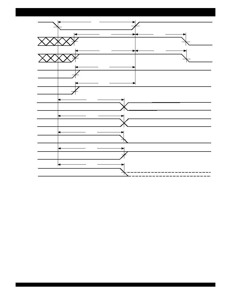
16
COMMERCIAL AND INDUSTRIAL TEMPERATURE RANGES
IDT72V295/72V2105 3.3V HIGH DENSITY CMOS
SUPERSYNC FIFO
TM
131,072 x 18, 262,144 x 18
Figure 6. Partial Reset Timing
t
RS
PRS
t
RSR
REN
t
RSS
4668 drw 09
t
RSR
WEN
t
RSS
RT
SEN
t
RSS
t
RSF
t
RSF
OE
= HIGH
OE
= LOW
PAE
PAF
,
HF
Q
0
- Q
n
t
RSF
EF
/
OR
FF
/
IR
t
RSF
t
RSF
If FWFT = HIGH,
OR
= HIGH
If FWFT = LOW,
EF
= LOW
If FWFT = LOW,
FF
= HIGH
If FWFT = HIGH,
IR
= LOW
t
RSS
17
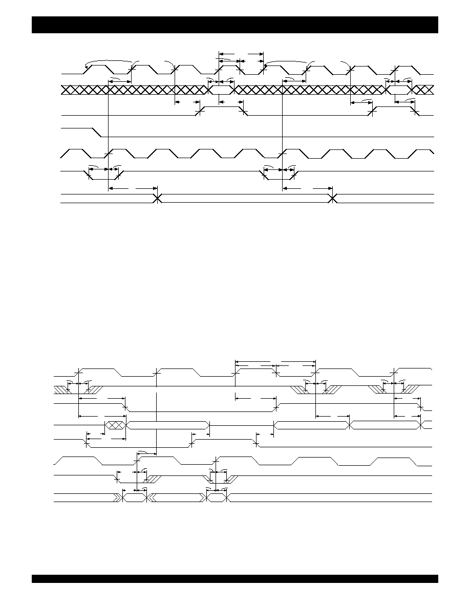
COMMERCIAL AND INDUSTRIAL TEMPERATURE RANGES
IDT72V295/72V2105 3.3V HIGH DENSITY CMOS
SUPERSYNC FIFO
TM
131,072 x 18, 262,144 x 18
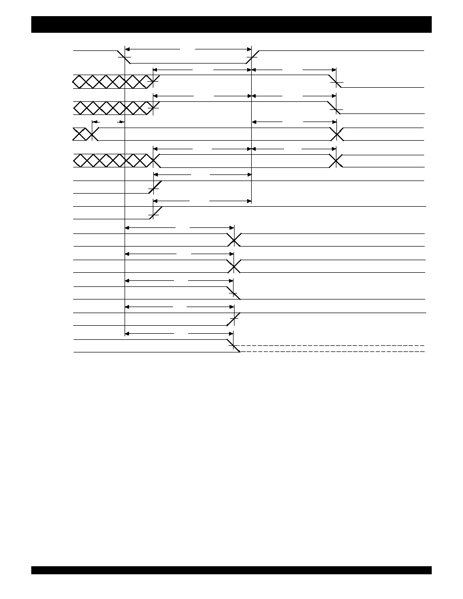
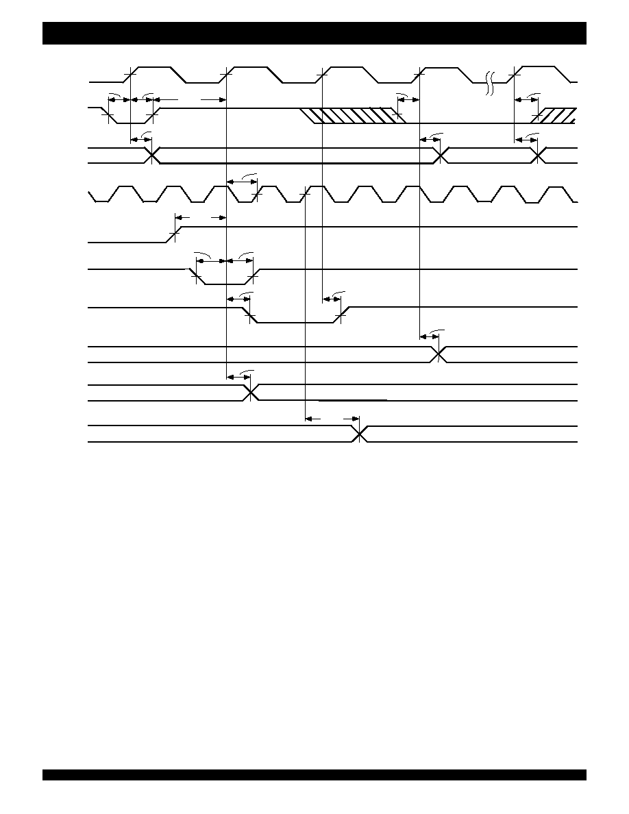
Figure 8. Read Cycle, Empty Flag and First Data Word Latency Timing (IDT Standard Mode)
NOTES:
1. t
SKEW1
is the minimum time between a rising WCLK edge and a rising RCLK edge to guarantee that
EF will go HIGH (after one RCLK cycle plus t
REF
). If the time between the rising edge
of WCLK and the rising edge of RCLK is less than t
SKEW1
, then
EF deassertion may be delayed one extra RCLK cycle.
2.
LD = HIGH.
3. First word latency: t
SKEW1
+ 1*T
RCLK
+ t
REF
.
NOTES:
1. t
SKEW1
is the minimum time between a rising RCLK edge and a rising WCLK edge to guarantee that
FF will go high (after one WCLK cycle pus t
WFF
). If the time between the rising
edge of the RCLK and the rising edge of the WCLK is less than t
SKEW1
, then the
FF deassertion may be delayed one extra WCLK cycle.
2.
LD = HIGH, OE = LOW, EF = HIGH.
Figure 7. Write Cycle and Full Flag Timing (IDT Standard Mode)
D
0
- D
n
WEN
RCLK
REN
t
ENH
t
ENH
Q
0
- Q
n
DATA READ
NEXT DATA READ
DATA IN OUTPUT REGISTER
t
SKEW1
(1)
4668 drw 10
WCLK
NO WRITE
1
2
1
2
t
DS
NO WRITE
t
WFF
t
WFF
t
WFF
t
A
t
ENS
t
ENS
t
SKEW1
(1)
t
DS
t
A
D
X
t
DH
t
CLK
t
CLKH
t
CLKL
D
X
+1
t
WFF
t
DH
FF
RCLK
REN
4668 drw 11
EF
t
CLK
t
CLKH
t
CLKL
t
ENH
t
REF
t
A
t
OLZ
t
OE
Q
0
- Q
n
OE
WCLK
t
SKEW1
(1)
WEN
D
0
- D
n
t
ENS
t
ENS
t
ENH
t
DS
t
DHS
D
0
1
2
t
OLZ
LAST WORD
D
0
D
1
D
1
t
ENS
t
ENH
t
DS
t
DH
t
OHZ
LAST WORD
t
REF
t
ENH
t
ENS
t
A
t
A
t
REF
t
ENS
t
ENH
NO OPERATION
NO OPERATION
18
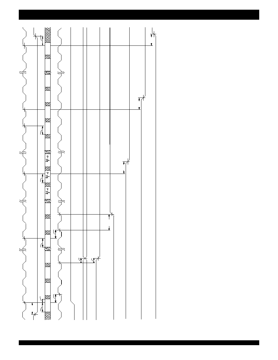
COMMERCIAL AND INDUSTRIAL TEMPERATURE RANGES
IDT72V295/72V2105 3.3V HIGH DENSITY CMOS
SUPERSYNC FIFO
TM
131,072 x 18, 262,144 x 18
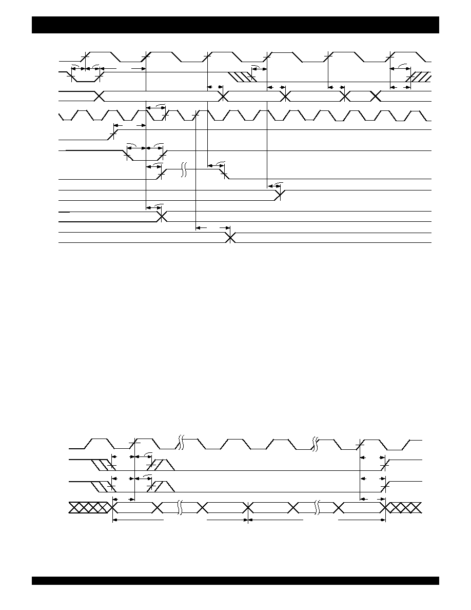
Figure 9. Write Timing (First Word Fall Through Mode)
NOTES:
1. t
SKEW1
is the minimum time between a rising WCLK edge and a rising RCLK edge to guarantee that
OR will go LOW after two RCLK cycles plus t
REF
. If the time between the rising edge of WCLK and the rising edge of RCLK is less than t
SKEW1
,
then
OR assertion may be delayed one extra RCLK cycle.
2. t
SKEW2
is the minimum time between a rising WCLK edge and a rising RCLK edge to guarantee that
PAE will go HIGH after one RCLK cycle plus t
PAE
. If the time between the rising edge of WCLK and the rising edge of RCLK is less than t
SKEW2
,
then the
PAE deassertion may be delayed one extra RCLK cycle.
3.
LD = HIGH, OE = LOW
4. n =
PAE offset, m = PAF offset and D = maximum FIFO depth.
5. D = 131,073 for IDT72V295 and 262,145 for IDT72V2105.
6. First word latency: t
SKEW1
+ 2*T
RCLK
+ t
REF
.
W
1
W
2
W
4
W
[n +2]
W
[D-m-1]
W
[D-m-2]
W
[D-1]
W
D
W
[n+3]
W
[n+4]
W
[D-m]
W
[D-m+1]
WCLK
WEN
D
0
- D
17
RCLK
t
DH
t
DS
t
SKEW1
(1)
REN
Q
0
- Q
17
PAF
HF
PAE
IR
t
DS
t
DS
t
DS
t
SKEW2
(2)
t
A
t
REF
OR
t
PAE
t
HF
t
WFF
W
[D-m+2]
W
1
t
ENH
4668 drw 12
DATA IN OUTPUT REGISTER
W
3
1
2
3
1
]
[
W
]
[
W
]
[
W
1
2
t
PAF
t
ENS
19
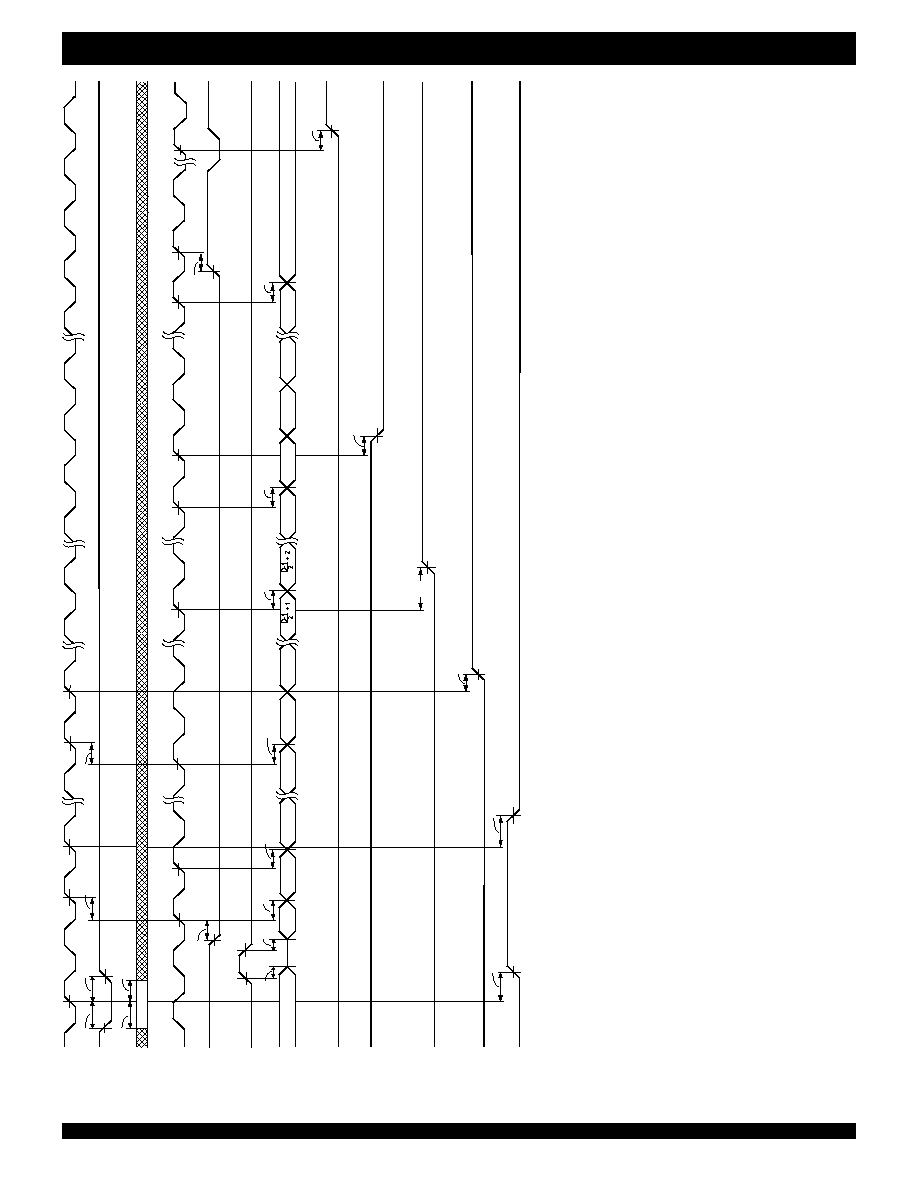
COMMERCIAL AND INDUSTRIAL TEMPERATURE RANGES
IDT72V295/72V2105 3.3V HIGH DENSITY CMOS
SUPERSYNC FIFO
TM
131,072 x 18, 262,144 x 18
Figure 10. Read Timing (First Word Fall Through Mode)
NOTES:
1. t
SKEW1
is the minimum time between a rising RCLK edge and a rising WCLK edge to guarantee that
IR will go LOW after one WCLK cycle plus t
WFF
. If the time between the rising edge of RCLK and the rising edge of WCLK is less than t
SKEW1
,
then the
IR assertion may be delayed one extra WCLK cycle.
2. t
SKEW2
is the minimum time between a rising RCLK edge and a rising WCLK edge to guarantee that
PAF will go HIGH after one WCLK cycle plus t
PAF
. If the time between the rising edge of RCLK and the rising edge of WCLK is less than
t
SKEW2
, then the
PAF deassertion may be delayed one extra WCLK cycle.
3.
LD = HIGH
4. n =
PAE Offset, m = PAF offset and D = maximum FIFO depth.
5. D = 131,073 for IDT72V295 and 262,145 for IDT72V2105.
WCLK
1
2
WEN
D
0
- D
17
RCLK
t
ENS
REN
Q
0
- Q
17
PAF
HF
PAE
IR
OR
W
1
W
1
W
2
W
3
W
m+2
W
[m+3]
t
OHZ
t
SKEW1
(1)
t
ENH
t
DS
t
OE
t
A
t
A
t
A
t
PAF
t
WFF
t
WFF
t
ENS
OE
t
SKEW2
(2)
W
D
4668 drw 13
t
PAE
W
[D-n]
W
[D-n-1]
t
A
t
A
t
HF
]
[
W
]
[
W
t
REF
W
[D-1]
W
D
t
A
W
[D-n+1]
W
[m+4]
W
[D-n+2]
t
ENS
1
t
DH
20
COMMERCIAL AND INDUSTRIAL TEMPERATURE RANGES
IDT72V295/72V2105 3.3V HIGH DENSITY CMOS
SUPERSYNC FIFO
TM
131,072 x 18, 262,144 x 18
NOTES:
1. Retransmit setup is complete after
EF returns HIGH, only then can a read operation begin.
2.
OE = LOW.
3. W
1
= first word written to the FIFO after Master Reset, W
2
= second word written to the FIFO after Master Reset.
4. No more than D - 2 may be written to the FIFO between Reset (Master or Partial) and Retransmit setup. Therefore,
FF will be HIGH throughout the Retransmit setup procedure.
D = 131,072 for IDT72V295 and 262,144 for IDT72V2105.
5. There must be at least two words written to the FIFO before a Retransmit operation can be invoked.
Figure 11. Retransmit Timing (IDT Standard Mode)
t
REF
t
RTS
t
ENH
4668 drw 14
t
A
t
ENS
W
x
WCLK
RCLK
REN
RT
EF
PAF
HF
PAE
Q
0
- Q
n
t
SKEW2
1
2
1
W
1
(3)
t
PAF
t
HF
t
PAE
t
REF
W
x+1
2
W
2
(3)
t
ENH
WEN
t
ENS
t
RTS
t
ENS
t
ENH
t
A
t
A
21
COMMERCIAL AND INDUSTRIAL TEMPERATURE RANGES
IDT72V295/72V2105 3.3V HIGH DENSITY CMOS
SUPERSYNC FIFO
TM
131,072 x 18, 262,144 x 18
NOTES:
1. Retransmit setup is complete after
OR returns LOW.
2. No more than D - 2 words may be written to the FIFO between Reset (Master or Partial) and Retransmit setup. Therefore,
IR will be LOW throughout the Retransmit setup
procedure. D = 131,073 for the IDT72V295 and
262,145 for the IDT72V2105.
3.
OE = LOW
4. W
1
, W
2
, W
3
= first, second and third words written to the FIFO after Master Reset.
5. There must be at least two words written to the FIFO before a Retransmit operation can be invoked.
Figure 12. Retransmit Timing (FWFT Mode)
Figure 13. Serial Loading of Programmable Flag Registers (IDT Standard and FWFT Modes)
NOTE:
1. X = 16 for the IDT72V295 and X = 17 for the IDT72V2105.
t
REF
t
RTS
t
ENH
4668 drw 15
t
ENS
W
x
WCLK
RCLK
REN
RT
OR
PAF
HF
PAE
Q
0
- Q
n
t
SKEW2
1
2
1
t
PAF
t
HF
t
PAE
t
REF
W
x+1
2
W
2
(4)
t
ENH
t
RTS
WEN
t
ENS
W
1
(4)
t
ENS
3
4
t
ENH
W
3
(4)
t
A
t
A
t
A
W
4
t
A
WCLK
SEN
SI
4668 drw 16
t
ENH
t
ENS
t
LDS
LD
t
DS
BIT 0
EMPTY OFFSET
BIT X
(1)
BIT 0
FULL OFFSET
t
ENH
BIT X
(1)
t
LDH
t
LDH
t
DH
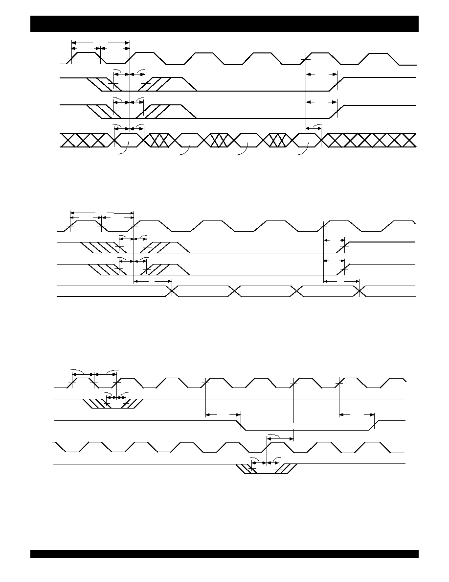
22
COMMERCIAL AND INDUSTRIAL TEMPERATURE RANGES
IDT72V295/72V2105 3.3V HIGH DENSITY CMOS
SUPERSYNC FIFO
TM
131,072 x 18, 262,144 x 18
NOTES:
1. m =
PAF offset .
2. D = maximum FIFO depth.
In IDT Standard mode: D = 131,072 for the IDT72V295 and 262,144 for the IDT72V2105.
In FWFT mode: D = 131,073 for the IDT72V295 and 262,145 for the IDT72V2105.
3. t
SKEW2
is the minimum time between a rising RCLK edge and a rising WCLK edge to guarantee that
PAF will go HIGH (after one WCLK cycle plus t
PAF
). If the time between the rising edge of
RCLK and the rising edge of WCLK is less than t
SKEW2
, then the
PAF deassertion time may be delayed one extra WCLK cycle.
4.
PAF is asserted and updated on the rising edge of WCLK only.
Figure 16. Programmable Almost-Full Flag Timing (IDT Standard and FWFT Modes)
NOTE:
1.
OE = LOW
Figure 15. Parallel Read of Programmable Flag Registers (IDT Standard and FWFT Modes)
Figure 14. Parallel Loading of Programmable Flag Registers (IDT Standard and FWFT Modes)
WCLK
t
ENH
t
CLKH
t
CLKL
WEN
PAF
RCLK
t
PAF
REN
4668 drw 19
t
ENS
t
ENH
t
ENS
D - (m+1) words in FIFO
(2)
t
PAF
D - m words in FIFO
(2)
t
SKEW2
(3)
1
2
1
2
D-(m+1) words
in FIFO
(2)
4668 drw 17
WCLK
LD
WEN
D
0
- D
15
t
LDS
t
ENS
PAE OFFSET
(LSB)
t
DS
t
DH
t
ENH
PAF OFFSET
(LSB)
PAF OFFSET
(MSB)
t
LDH
t
CLK
t
DH
t
CLKH
t
CLKL
t
ENH
PAE OFFSET
(MSB)
t
LDH
4668 drw 18
RCLK
LD
REN
Q
0
- Q
15
t
LDH
t
LDS
t
ENS
DATA IN OUTPUT REGISTER
t
ENH
t
ENH
t
LDH
t
CLK
t
A
t
A
t
CLKH
t
CLKL
PAF OFFSET
(MSB)
PAF OFFSET
(LSB)
PAE OFFSET
(MSB)
PAE OFFSET
(LSB)
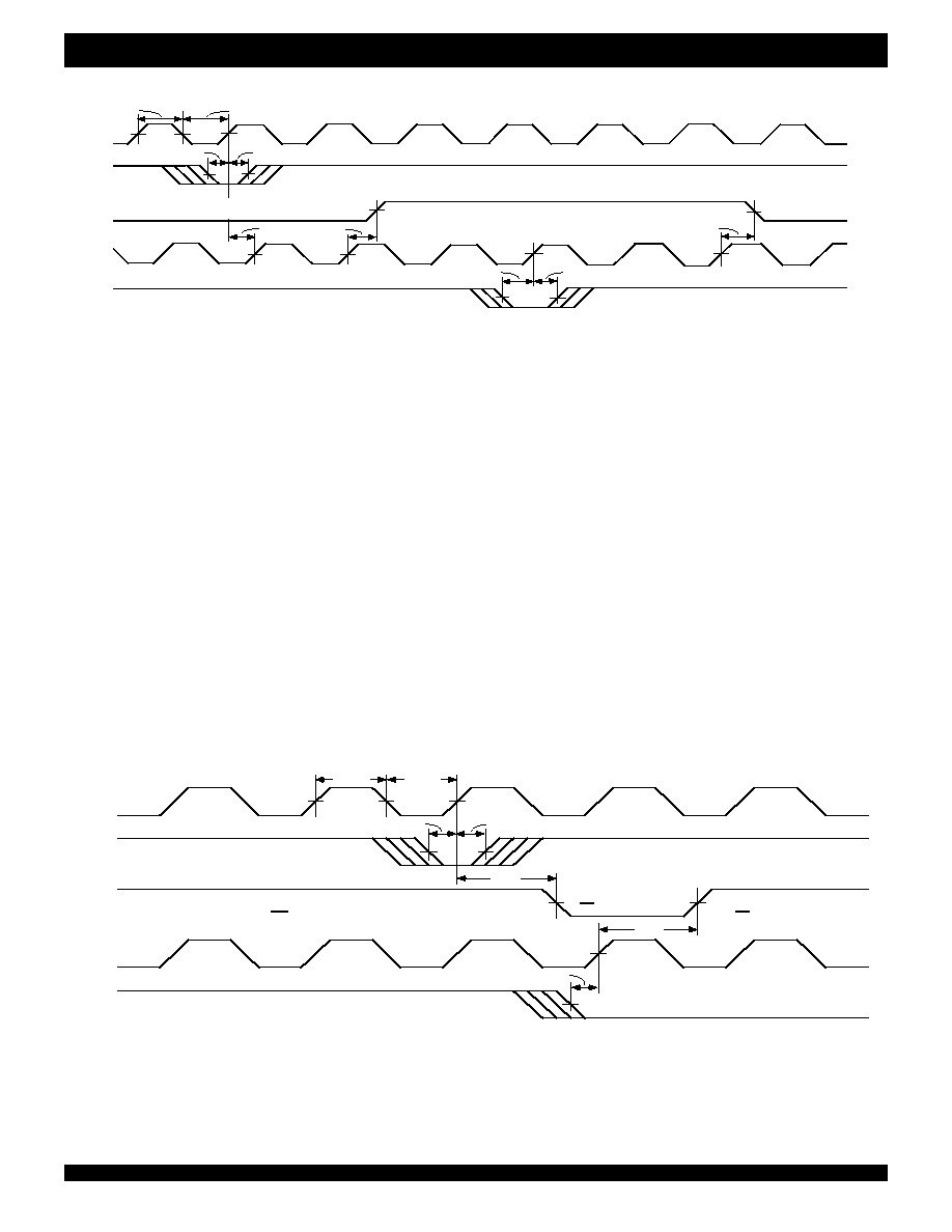
23
COMMERCIAL AND INDUSTRIAL TEMPERATURE RANGES
IDT72V295/72V2105 3.3V HIGH DENSITY CMOS
SUPERSYNC FIFO
TM
131,072 x 18, 262,144 x 18
NOTES:
1. For IDT Standard mode: D = maximum FIFO depth. D = 131,072 for the IDT72V295 and 262,144 for the IDT72V2105.
2. For FWFT mode: D = maximum FIFO depth. D = 131,073 for the IDT72V295 and 262,145 for the IDT72V2105.
NOTES:
1. n =
PAE offset.
2. For IDT Standard mode
3. For FWFT mode.
4. t
SKEW2
is the minimum time between a rising WCLK edge and a rising RCLK edge to guarantee that
PAE will go HIGH (after one RCLK cycle plus t
PAE
). If the time between the rising edge of
WCLK and the rising edge of RCLK is less than t
SKEW2
, then the
PAE deassertion may be delayed one extra RCLK cycle.
5.
PAE is asserted and updated on the rising edge of WCLK only.
Figure 18. Half-Full Flag Timing (IDT Standard and FWFT Modes)
Figure 17. Programmable Almost-Empty Flag Timing (IDT Standard and FWFT Modes)
WCLK
t
ENH
t
CLKH
t
CLKL
WEN
PAE
RCLK
t
ENS
n words in FIFO
(2)
,
n+1 words in FIFO
(3)
t
PAE
t
SKEW2
(4)
t
PAE
1
2
1
2
REN
4668 drw 20
t
ENS
t
ENH
n+1 words in FIFO
(2)
,
n+2 words in FIFO
(3)
n words in FIFO
(2)
,
n+1 words in FIFO
(3)
WCLK
t
ENS
t
ENH
WEN
HF
t
ENS
t
HF
RCLK
t
HF
REN
4668 drw 21
t
CLKL
t
CLKH
D/2 words in FIFO
(1)
,
[
+ 1
]
words in FIFO
(2)
D -1
2
D/2 + 1 words in FIFO
(1)
,
[
+ 2
]
words in FIFO
(2)
D-1
2
D/2 words in FIFO
(1)
,
[
+ 1
]
words in FIFO
(2)
D-1
2
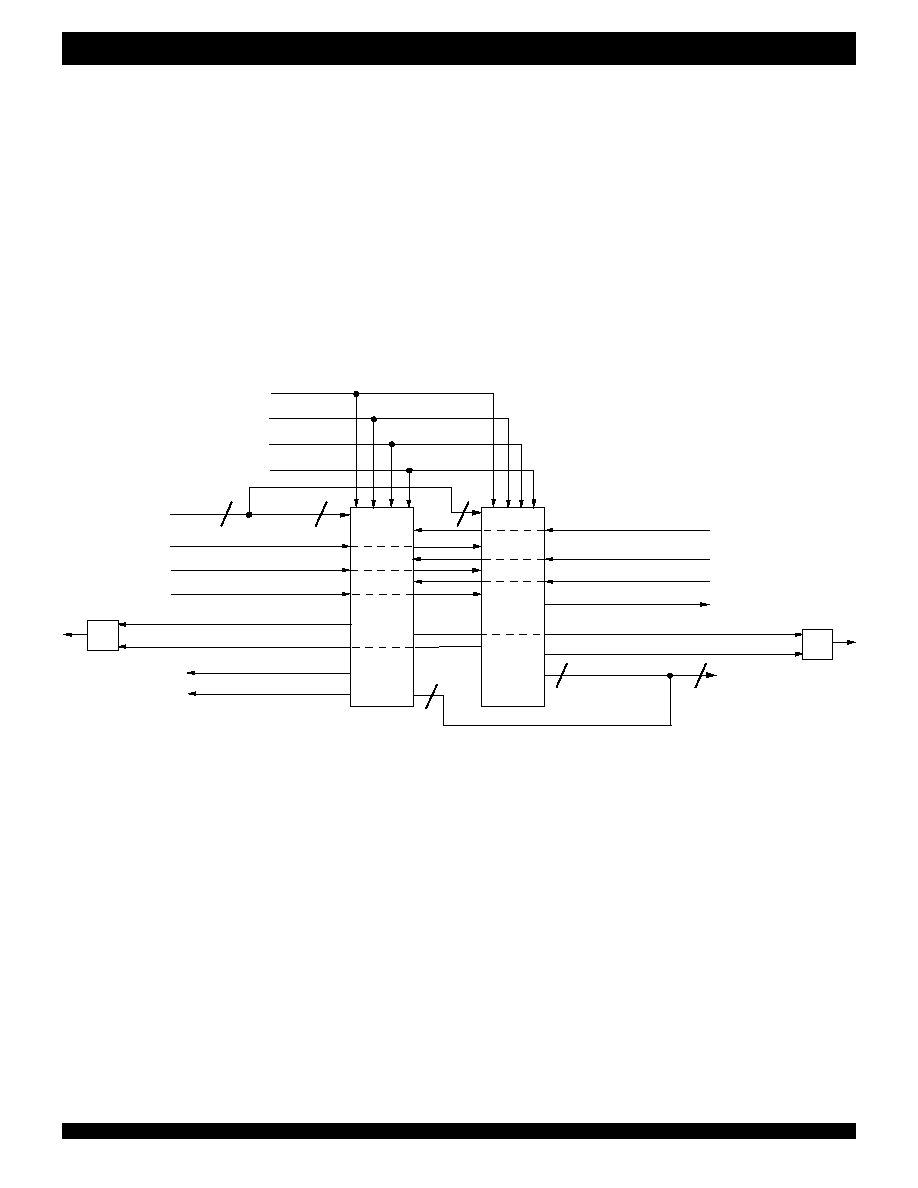
24
COMMERCIAL AND INDUSTRIAL TEMPERATURE RANGES
IDT72V295/72V2105 3.3V HIGH DENSITY CMOS
SUPERSYNC FIFO
TM
131,072 x 18, 262,144 x 18
NOTES:
1. Use an AND gate in IDT Standard mode, an OR gate in FWFT mode.
2. Do not connect any output control signals directly together.
3. FIFO #1 and FIFO #2 must be the same depth, but may be different word widths.
OPTIONAL CON.IGURATIONS
WIDTH EXPANSION CONFIGURATION
Word width may be increased simply by connecting together the control
signals of multiple devices. Status flags can be detected from any one
device. The exceptions are the
EF and FF functions in IDT Standard mode
and the
IR and OR functions in FWFT mode. Because of variations in skew
between RCLK and WCLK, it is possible for
EF/FF deassertion and IR/OR
assertion to vary by one cycle between FIFOs. In IDT Standard mode, such
Figure 19. Block Diagram of 131,072 x 36 and 262,144 x 36 Width Expansion
problems can be avoided by creating composite flags, that is, ANDing
EF
of every FIFO, and separately ANDing
FF of every FIFO. In FWFT mode,
composite flags can be created by ORing
OR of every FIFO, and separately
ORing
IR of every FIFO.
Figure 23 demonstrates a width expansion using two IDT72V295/
72V2105 devices. D
0
-D
17
from each device form a 36-bit wide input bus
and Q
0
-Q
17
from each device form a 36-bit wide output bus. Any word width
can be attained by adding additional IDT72V295/72V2105 devices.
WRITE CLOCK (WCLK)
m + n
m
n
MASTER RESET (
MRS
)
READ CLOCK (RCLK)
DATA OUT
n
m + n
WRITE ENABLE (
WEN
)
FULL FLAG/INPUT READY (
FF
/
IR
) #1
PROGRAMMABLE (
PAF
)
PROGRAMMABLE (
PAE
)
E
MPTY FLAG/OUTPUT READY (
EF
/
OR
)
#2
OUTPUT ENABLE (
OE
)
READ ENABLE (
REN
)
m
LOAD (
LD
)
IDT
72V295
72V2105
EMPTY FLAG/OUTPUT READY (
EF
/
OR
)
#1
PARTIAL RESET (
PRS
)
IDT
72V295
72V2105
4668 drw 22
FULL FLAG/INPUT READY (
FF
/
IR
) #2
HALF-FULL FLAG (
HF
)
FIRST WORD FALL THROUGH/
SERIAL INPUT (FWFT/SI)
RETRANSMIT (
RT
)
FIFO
#2
GATE
(1)
GATE
(1)
D
0
-
Dm
DATA IN
Dm
+1
- Dn
Q
0
-
Qm
Qm
+1
- Qn
FIFO
#1
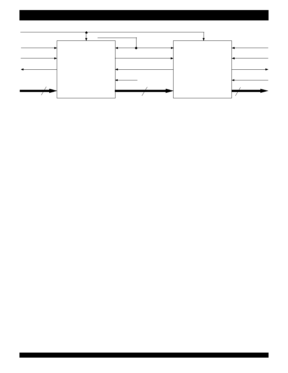
25
COMMERCIAL AND INDUSTRIAL TEMPERATURE RANGES
IDT72V295/72V2105 3.3V HIGH DENSITY CMOS
SUPERSYNC FIFO
TM
131,072 x 18, 262,144 x 18
Figure 20. Block Diagram of 262,144 x 18 and 524,288 x 18 Depth Expansion
Dn
INPUT READY
WRITE ENABLE
WRITE CLOCK
WEN
WCLK
IR
DATA IN
RCLK
READ CLOCK
RCLK
REN
OE
OUTPUT ENABLE
OUTPUT READY
Qn
Dn
IR
GND
WEN
WCLK
OR
REN
OE
Qn
READ ENABLE
OR
DATA OUT
IDT
72V295
72V2105
TRANSFER CLOCK
4668 drw 23
n
n
n
FWFT/SI
FWFT/SI
FWFT/SI
IDT
72V295
72V2105
DEPTH EXPANSION CONFIGURATION (FWFT MODE ONLY)
The IDT72V295 can easily be adapted to applications requiring depths
greater than 131,072 and 262,144 for the IDT72V2105 with an 18-bit bus
width. In FWFT mode, the FIFOs can be connected in series (the data
outputs of one FIFO connected to the data inputs of the next) with no
external logic necessary. The resulting configuration provides a total depth
equivalent to the sum of the depths associated with each single FIFO.
Figure 24 shows a depth expansion using two IDT72V295/72V2105 de-
vices.
Care should be taken to select FWFT mode during Master Reset for all
FIFOs in the depth expansion configuration. The first word written to an
empty configuration will pass from one FIFO to the next ("ripple down") until
it finally appears at the outputs of the last FIFO in the chain≠no read
operation is necessary but the RCLK of each FIFO must be free-running.
Each time the data word appears at the outputs of one FIFO, that device's
OR line goes LOW, enabling a write to the next FIFO in line.
For an empty expansion configuration, the amount of time it takes for
OR
of the last FIFO in the chain to go LOW (i.e. valid data to appear on the last
FIFO's outputs) after a word has been written to the first FIFO is the sum of
the delays for each individual FIFO:
(N ≠ 1)*(4*transfer clock) + 3*T
RCLK
where N is the number of FIFOs in the expansion and T
RCLK
is the RCLK
period. Note that extra cycles should be added for the possibility that the
t
SKEW1
specification is not met between WCLK and transfer clock, or RCLK
and transfer clock, for the
OR flag.
The "ripple down" delay is only noticeable for the first word written to an
empty depth expansion configuration. There will be no delay evident for
subsequent words written to the configuration.
The first free location created by reading from a full depth expansion
configuration will "bubble up" from the last FIFO to the previous one until it
finally moves into the first FIFO of the chain. Each time a free location is
created in one FIFO of the chain, that FIFO's
IR line goes LOW, enabling the
preceding FIFO to write a word to fill it.
For a full expansion configuration, the amount of time it takes for
IR of the
first FIFO in the chain to go LOW after a word has been read from the last
FIFO is the sum of the delays for each individual FIFO:
(N ≠ 1)*(3*transfer clock) + 2 T
WCLK
where N is the number of FIFOs in the expansion and T
WCLK
is the WCLK
period. Note that extra cycles should be added for the possibility that the
t
SKEW1
specification is not met between RCLK and transfer clock, or WCLK
and transfer clock, for the
IR flag.
The Transfer Clock line should be tied to either WCLK or RCLK,
whichever is faster. Both these actions result in data moving, as quickly as
possible, to the end of the chain and free locations to the beginning of the
chain.
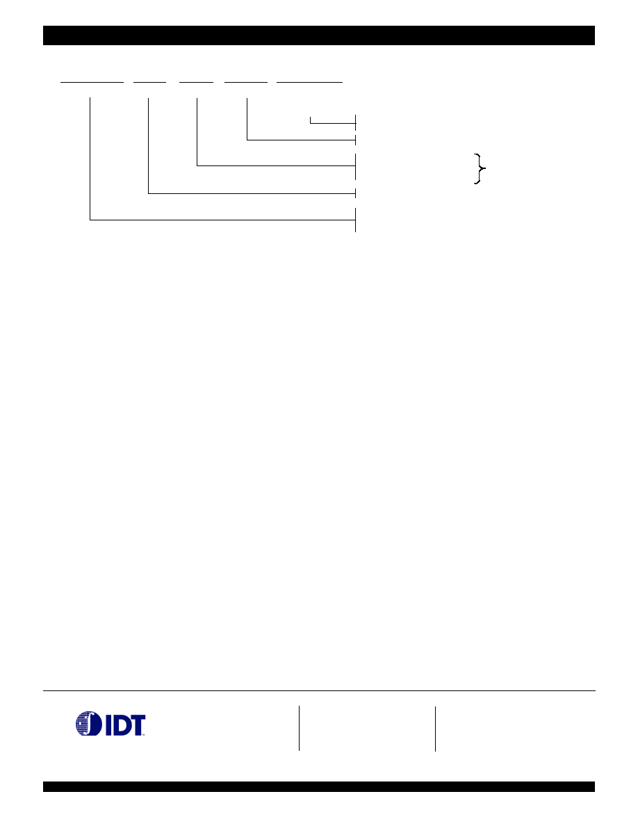
26
*To search for sales office near you, please click the sales button found on our home page or dial the 800# above and press 2.
The SuperSync FIFO is a trademark and the IDT logo is a registered trademark of Integrated Device Technology, Inc.
CORPORATE HEADQUARTERS
for SALES:
for Tech Support:
2975 Stender Way
800-345-7015 or 408-727-6116
408-330-1753
Santa Clara, CA 95054
fax: 408-492-8674
email:FIFOhelp@idt.com
www.idt.com*
PF Pkg: www.idt.com/docs/PSC4036.pdf
ORDERING IN.ORMATION
Thin Plastic Quad Flatpack (TQFP, PN64-1)
Commercial (0
∞
C to +70
∞
C)
Low Power
131,072 x 18
3.3V SuperSyncFIFO
4668 drw24
Clock Cycle Time (t
CLK
)
Commercial Only
IDT
XXXXX
Device Type
X
Power
XX
Speed
X
Package
X
Process /
Temperature
Range
BLANK
72V295
I
(1)
Industrial (-40
∞
C to +85
∞
C)
PF
10
15
20
Com'l & Ind'l
Commercial Only
Speed in Nanoseconds
L
72V2105
262,144 x 18
3.3V SuperSyncFIFO
NOTE:
1. Industrial temperature range is available as a standard device for 15ns.
DATASHEET DOCUMENT HISTORY
9/12/2000
pg. 5.
12/18/2000
pgs. 5, 6 and 26.
03/27/2001
pgs 6 and 26.