 | –≠–ª–µ–∫—Ç—Ä–æ–Ω–Ω—ã–π –∫–æ–º–ø–æ–Ω–µ–Ω—Ç: 72V3611 | –°–∫–∞—á–∞—Ç—å:  PDF PDF  ZIP ZIP |
1
MAY 2003
3.3 VOLT CMOS SyncFIFO
TM
64 x 36
IDT72V3611
2003 Integrated Device Technology, Inc. All rights reserved. Product specifications subject to change without notice.
DSC-4657/1
IDT and the IDT logo are registered trademarks of Integrated Device Technology, Inc. SyncFIFO is a trademark of Integrated Device Technology, Inc.
COMMERCIAL TEMPERATURE RANGE
FEATURES:
∑
∑
∑
∑
∑
64 x 36 storage capacity
∑
∑
∑
∑
∑
Supports clock frequencies up to 67MHz
∑
∑
∑
∑
∑
Fast access times of 10ns
∑
∑
∑
∑
∑
Free-running CLKA and CLKB may be asynchronous or
coincident (permits simultaneous reading and writing of
data on a single clock edge)
∑
∑
∑
∑
∑
Synchronous data buffering from Port A to Port B
∑
∑
∑
∑
∑
Mailbox bypass register in each direction
∑
∑
∑
∑
∑
Programmable Almost-Full (
AF) and Almost-Empty (AE) flags
∑
∑
∑
∑
∑
Microprocessor Interface Control Logic
∑
∑
∑
∑
∑
Full Flag (
FF) and Almost-Full (AF) flags synchronized by CLKA
∑
∑
∑
∑
∑
Empty Flag (
EF) and Almost-Empty (AE) flags synchronized by
CLKB
∑
∑
∑
∑
∑
Passive parity checking on each Port
∑
∑
∑
∑
∑
Parity Generation can be selected for each Port
∑
∑
∑
∑
∑
Available in 132-pin Plastic Quad Flatpack (PQF) or space-saving
120-pin Thin Quad Flatpack (PF)
∑
∑
∑
∑
∑
Industrial temperature range (≠40
∞∞
∞∞
∞C to +85∞∞∞∞∞C) is available
∑
∑
∑
∑
∑
Pin and functionally compatible version of the 5V operating
IDT723611
DESCRIPTION:
The IDT72V3611 is a pin and functionally compatible version of the
IDT723611, designed to run off a 3.3V supply for exceptionally low power
consumption. This device is a monolithic, high-speed, low-power, CMOS
Synchronous (clocked) FIFO memory which supports clock frequencies up to
67MHz and has read access times as fast as 10ns. The 64 x 36 dual-port FIFO
buffers data from Port A to Port B. The FIFO operates in IDT Standard mode
and has flags to indicate empty and full conditions, and two programmable flags,
Almost-Full (
AF) and Almost-Empty (AE), to indicate when a selected number
of words is stored in memory. Communication between each port can take place
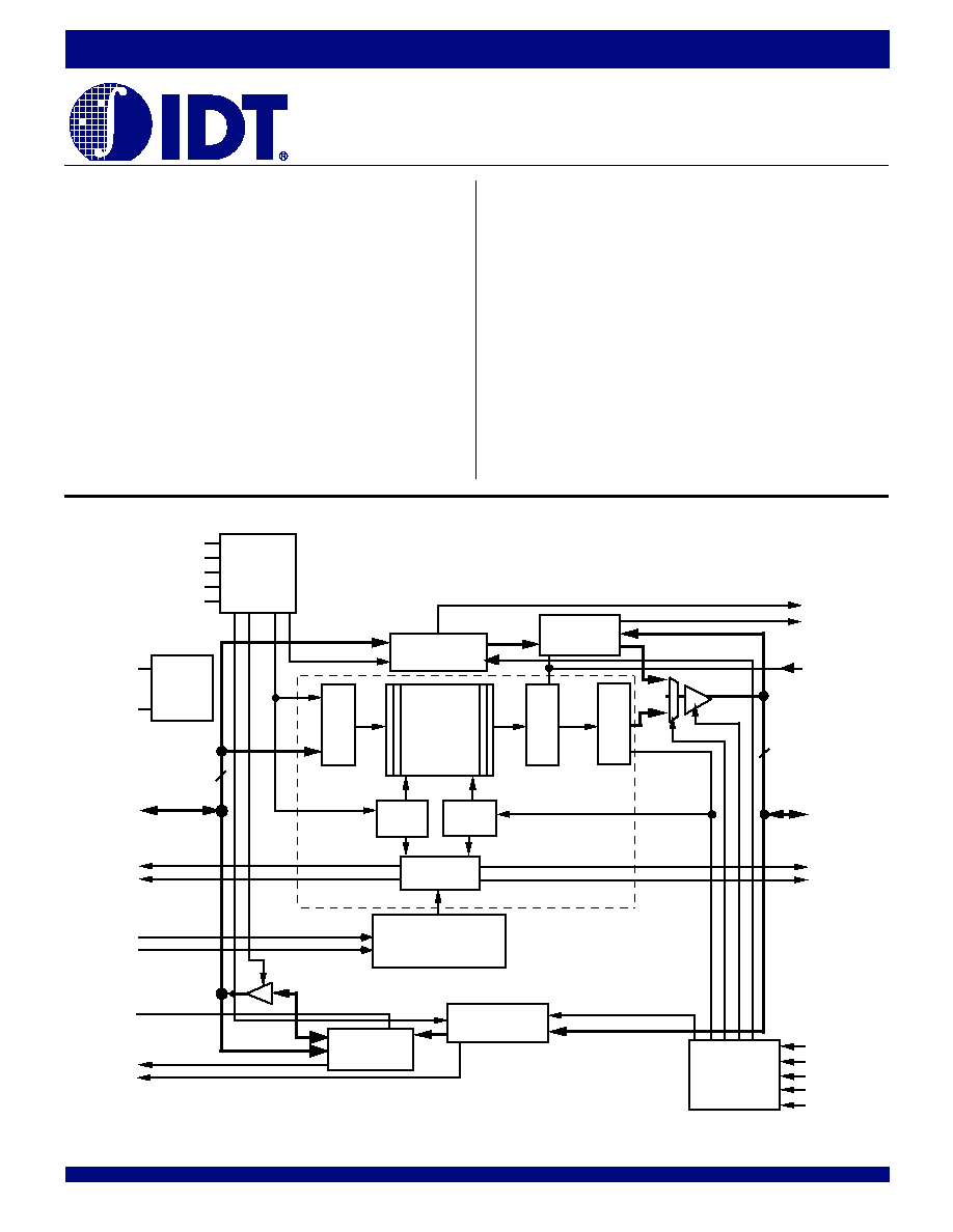
FUNCTIONAL BLOCK DIAGRAM
Mail 2
Register
Mail 1
Register
Input
Register
Output
Register
Write
Pointer
Read
Pointer
Status Flag
Logic
CLKA
CSA
W/
RA
ENA
MBA
Port-A
Control
Logic
Reset
Logic
RST
PEFA
MBF2
CLKB
CSB
W/
RB
ENB
MBB
Port-B
Control
Logic
MBF1
EF
AE
36
B
0
- B
35
FF
AF
FS
0
FS
1
4657 drw01
Programmable
Flag Offset
Registers
A
0
- A
35
Parity
Gen/Check
Parity
Generation
FIFO
ODD/
EVEN
PGA
Parity
Gen/Check
PGB
PEFB
36
RAM
ARRAY
64 x 36

2
IDT72V3611 3.3V, CMOS SyncFIFO
TM
64 x 36
COMMERCIAL TEMPERATURE RANGE
DESCRIPTION (CONTINUED)
NOTE:
1. NC = No internal connection
TQFP (PN120-1, order code: PF)
TOP VIEW
PIN CONFIGURATION
4657 drw 02
A
23
A
22
A
21
GND
A
20
A
19
A
18
A
17
A
16
A
15
A
14
A
13
A
12
A
11
A
10
GND
A
9
A
8
A
7
V
CC
A
6
A
5
A
4
A
3
GND
A
2
A
1
A
0
NC
NC
1
2
3
4
5
6
7
8
9
10
11
12
13
14
15
16
17
18
19
20
21
22
23
24
25
26
27
28
29
30
B
22
B
21
GND
B
20
B
19
B
18
B
17
B
16
B
15
B
14
B
13
B
12
B
11
B
10
GND
B
9
B
8
B
7
V
CC
B
6
B
5
B
4
B
3
GND
B
2
B
1
B
0
EF
AE
NC
90
89
88
87
86
85
84
83
82
81
80
79
78
77
76
75
74
73
72
71
70
69
68
67
66
65
64
63
62
61
AF FF
CSA ENA
CLKA
W/
R
A
V
CC
PGA
PEFA MBF2 MBA
FS
1
FS
0
ODD/
EVEN
RST GND
NC
NC
NC
NC
MBB
MBF1 PEFB PGB
V
CC
W/
R
B
CLKB
ENB
CSB NC
31
32
33 34
35
36
37
38
39
40
41
42 43
44
45
46
47
48 49
50
51
52
53
54
55
56
57
58
59
60
91
120
119
118
117
116
115
114
113
112
111
110
109
108
107
106
105
104
103
102
101
100
99
98
97
96
95
94
93
92
B
23
A
24
A
25
A
26
V
CC
A
27
A
28
A
29
GND
A
30
A
31
A
34
A
35
B
35
GND
B
34
B
33
B
32
B
30
B
31
GND
B
29
B
28
B
27
V
CC
B
26
B
25
B
24
A
32
A
33
through two 36-bit mailbox registers. Each mailbox register has a flag to signal
when new mail has been stored. Parity is checked passively on each port and
may be ignored if not desired. Parity generation can be selected for data read
from each port. Two or more devices may be used in parallel to create wider
data paths.
The IDT72V3611 is a synchronous (clocked) FIFO, meaning each port
employs a synchronous interface. All data transfers through a port are gated
to the LOW-to-HIGH transition of a port clock by enable signals. The clocks for
each port are independent of one another and can be asynchronous or
coincident. The enables for each port are arranged to provide a simple
bidirectional interface between microprocessors and/or buses with synchro-
nous control.
The Full Flag (
FF) and Almost-Full (AF) flag of the FIFO are two-stage
synchronized to the port clock that writes data into its array (CLKA). The Empty
Flag (
EF) and Almost-Empty (AE) flag of the FIFO are two-stage synchronized
to the port clock that reads data from its array.
The IDT72V3611 is characterized for operation from 0
∞C to 70∞C. Industrial
temperature range (≠40
∞C to +85∞C) is available by special order. This device
is fabricated using IDT's high speed, submicron CMOS technology.

3
IDT72V3611 3.3V, CMOS SyncFIFO
TM
64 x 36
COMMERCIAL TEMPERATURE RANGE
PQFP (PQ132-1, order code: PQF)
TOP VIEW
GND
AE
EF
B
0
B
1
B
2
GND
B
3
B
4
B
5
B
6
V
CC
B
7
B
8
B
9
GND
B
10
B
11
V
CC
B
12
B
13
B
14
GND
B
15
B
16
B
17
B
18
B
19
B
20
GND
B
21
B
22
B
23
GND
NC
NC
A
0
A
1
A
2
GND
A
3
A
4
A
5
A
6
V
CC
A
7
A
8
A
9
GND
A
10
A
11
V
CC
A
12
A
13
A
14
GND
A
15
A
16
A
17
A
18
A
19
A
20
GND
A
21
A
22
A
23
18
19
20
21
22
23
24
25
26
27
28
29
30
31
32
33
34
35
36
37
38
39
40
41
42
43
44
45
46
47
48
49
50
116
115
114
113
112
111
110
109
108
107
106
105
104
103
102
101
100
99
98
97
96
95
94
93
92
91
90
89
88
87
86
85
84
4657 drw 03
117
17
16
15
14
13
12
11
10
9
7
6
5
4
3
2
1
132
131
130
129
128
127
126
125
124
123
122
121
120
119
118
8
V
CC
V
CC
A
24
A
25
A
26
A
27
GND
A
28
A
29
V
CC
A
30
A
31
A
32
GND
A
33
A
34
A
35
GND
B
35
B
34
B
33
GND
B
32
B
31
B
30
V
CC
B
29
B
28
B
27
GND
B
26
B
25
B
24
51
52
53
54
55
56
57
58
59
60
61
62
63
64
65
66
67
68
69
70
71
72
73
74
75
76
77
78
79
80
81
82
83
NC
AF FF CSA ENA CLKA W/
R
A
V
CC
PGA
FS
0
ODD/
EVEN
FS
1
PEFA
MBF2
RST
NC
GND
NC
NC
NC
MBF1 GND PEFB
V
CC
W/
R
B
CLKB
ENB
CSB NC
GND
MBA
MBB
PGB
*
*
Electrical pin 1 in center of beveled edge. Pin 1 identifier in corner.
PIN CONFIGURATION (CONTINUED)
NOTE:
1. NC = No internal connection

4
IDT72V3611 3.3V, CMOS SyncFIFO
TM
64 x 36
COMMERCIAL TEMPERATURE RANGE
Symbol
Name
I/O
Description
A0-A35
Port-A Data
I/O
36-bit bidirectional data port for side A.
AE
Almost-Empty Flag
O
Programmable Almost-Empty flag synchronized to CLKB. It is LOW when the number of words
in the FIFO is less than or equal to the value in the offset register, X.
AF
Almost-Full Flag
O
Programmable Almost-Full flag synchronized to CLKA. It is LOW when the number of empty
locations in the FIFO is less than or equal to the value in the Offset register, X.
B0-B35
Port-B Data.
I/O
36-bit bidirectional data port for side B.
CLKA
Port-A Clock
I
CLKA is a continuous clock that synchronizes all data transfers through port-A and can be
asynchronous or coincident to CLKB.
FF and AF are synchronized to the LOW-to-HIGH
transition of CLKA.
CLKB
Port-B Clock
I
CLKB is a continuous clock that synchronizes all data transfers through port-B and can be
asynchronous or coincident to CLKA.
EF and AE are synchronized to the LOW-to-HIGH
transition of CLKB.
CSA
Port-A Chip Select
I
CSA must be LOW to enable a LOW-to-HIGH transition of CLKA to read or write data on port-A.
The A0-A35 outputs are in the high-impedance state when
CSA is HIGH.
CSB
Port-B Chip Select
I
CSB must be LOW to enable a LOW-to-HIGH transition of CLKB to read or write data on port-B.
The B0-B35 outputs are in the high-impedance state when
CSB is HIGH.
EF
Empty Flag
O
EF is synchronized to the LOW-to-HIGH transition of CLKB. When EF is LOW, the FIFO is empty,
and reads from its memory are disabled. Data can be read from the FIFO to its output register
when
EF is HIGH. EF is forced LOW when the device is reset and is set HIGH by the second
LOW-to-HIGH transition of CLKB after data is loaded into empty FIFO memory.
ENA
Port-A Enable
I
ENA must be HIGH to enable a LOW-to-HIGH transition of CLKA to read or write data on port-A.
ENB
Port-B Enable
I
ENB must be HIGH to enable a LOW-to-HIGH transition of CLKB to read or write data on port-B.
FF
Full Flag
O
FF is synchronized to the LOW-to-HIGH transition of CLKA. When FF is LOW, the FIFO is full, and
writes to its memory are disabled.
FF is forced LOW when the device is reset and is set HIGH by
the second LOW-to-HIGH transition of CLKA after reset.
FS1, FS0
Flag-Offset Selects
I
The LOW-to-HIGH transition of
RST latches the values of FS0 and FS1, which loads one of four
preset values into the Almost-Full and Almost-Empty Offset register (X).
MBA
Port-A Mailbox Select
I
A HIGH level on MBA chooses a mailbox register for a port-A read or write operation.
MBB
Port-B Mailbox Select
I
A HIGH level on MBB chooses a mailbox register for a port-B read or write operation. When the
B0-B35 outputs are active, a HIGH level on MBB selects data from the mail1 register for output,
and a LOW level selects the FIFO output register data for output.
MBF1
Mail1 Register Flag
O
MBF1 is set LOW by a LOW-to-HIGH transition of CLKA that writes data to the mail1 register. Writes
to the mail1 register are inhibited while
MBF1 is set LOW. MBF1 is set HIGH by a LOW-to-HIGH
transition of CLKB when a port-B read is selected and MBB is HIGH.
MBF1 is set HIGH when the
device is reset.
MBF2
Mail2 Register Flag
O
MBF2 is set LOW by a LOW-to-HIGH transition of CLKB that writes data to the mail2 register. Writes
to the mail2 register are inhibited while
MBF2 is LOW. MBF2 is set HIGH by a LOW-to-HIGH
transition of CLKA when a port-A read is selected and MBA is HIGH.
MBF2 is set HIGH when the
device is reset.
ODD/
Odd/Even Parity
I
Odd parity is checked on each port when ODD/
EVEN is HIGH, and even parity is checked when
EVEN
Select
ODD/
EVEN is LOW. ODD/EVEN also selects the type of parity generated for each port if parity
generation is enabled for a read operation.
PEFA
Port-A Parity Error
O
When any byte applied to terminals A0-A35 fails parity,
PEFA is LOW. Bytes are organized as
Flag
[Port A)
A0-A8, A9-A17, A18-A26, and A27-A35, with the most significant bit of each byte serving as the
parity bit. The type of parity checked is determined by the state of the ODD/
EVEN input. The
parity trees used to check the A0-A35 inputs are shared by the mail2 register to generate parity if
parity generation is selected by PGA. Therefore, if a mail2 read with parity generation is setup by
having
CSA LOW, ENA HIGH, W/RA LOW, MBA HIGH, and PGA HIGH, the PEFA flag is forced
HIGH regardless of the state of A0-A35 inputs.
PIN DESCRIPTION
5
IDT72V3611 3.3V, CMOS SyncFIFO
TM
64 x 36
COMMERCIAL TEMPERATURE RANGE
PIN DESCRIPTION (CONTINUED)
Symbol
Name
I/O
Description
PEFB
Port-B Parity Error
O
When any byte applied to terminals B0-B35 fails parity,
PEFB is LOW. Bytes are organized as
Flag
(Port B)
B0-B8, B9-B17, B18-B26, B27-B35, with the most significant bit of each byte serving as the parity
bit. The type of parity checked is determined by the state of the ODD/
EVEN input. The parity
trees used to check the B0-B35 inputs are shared by the mail1 register to generate parity if parity
generation is selected by PGB. Therefore, if a mail1 read with parity generation is setup by
having
CSB LOW, ENB HIGH, W/RB LOW, MBB HIGH, and PGB HIGH, the PEFB flag is forced
HIGH regardless of the state of the B0-B35 inputs
PGA
Port-A Parity
I
Parity is generated for mail2 register reads from port A when PGA is HIGH. The type of parity
Generation
generated is selected by the state of the ODD/
EVEN input. Bytes are organized as A0-A8,
A9-A17, A18-A26, and A27-A35. The generated parity bits are output in the most significant bit
of each byte.
PGB
Port-B Parity
I
Parity is generated for data reads from port B when PGB is HIGH. The type of parity generated
Generation
is selected by the state of the ODD/
EVEN input. Bytes are organized as B0-B8, B9-B17,
B18-B26, and B27-B35. The generated parity bits are output in the most significant bit of
each byte.
RST
Reset
I
To reset the device, four LOW-to-HIGH transitions of CLKA and four LOW-to-HIGH transitions of
CLKB must occur while
RST is LOW. This sets the AF, MBF1, and MBF2 flags HIGH and the
EF, AE, and FF flags LOW. The LOW-to-HIGH transition of RST latches the status of the FS1
and FS0 inputs to select Almost-Full and Almost-Empty flag offset.
W/
RA
Port-A Write/Read
I
A HIGH selects a write operation and a LOW selects a read operation on port A for a
Select
LOW-to-HIGH transition of CLKA. The A0-A35 outputs are in the high-impedance state
when W/
RA is HIGH.
W/
RB
Port-B Write/Read
I
A HIGH selects a write operation and a LOW selects a read operation on port B for a
Select
LOW-to-HIGH transition of CLKB. The B0-B35 outputs are in the high-impedance state
when W/
RB is HIGH.

6
IDT72V3611 3.3V, CMOS SyncFIFO
TM
64 x 36
COMMERCIAL TEMPERATURE RANGE
ABSOLUTE MAXIMUM RATINGS OVER OPERATING FREE-AIR
TEMPERATURE RANGE (Unless otherwise noted)
(1)
Symbol
Rating
Commercial
Unit
V
CC
Supply Voltage Range
≠0.5 to +4.6
V
V
I
(2)
Input Voltage Range
≠0.5 to V
CC
+0.5
V
V
O
(2)
Output Voltage Range
≠0.5 to V
CC
+0.5
V
I
IK
Input Clamp Current, (V
I
< 0 or V
I
> V
CC
)
±20
mA
I
OK
Output Clamp Current, (V
O
= < 0 or V
O
> V
CC
)
±50
mA
I
OUT
Continuous Output Current, (V
O
= 0 to V
CC
)
±50
mA
I
CC
Continuous Current Through V
CC
or GND
±500
mA
T
STG
Storage Temperature Range
≠65 to 150
∞C
NOTES:
1. Stresses beyond those listed under "Absolute Maximum Ratings" may cause permanent damage to the device. These are stress ratings only and functional operation of the device at
these or any other conditions beyond those indicated under "Recommended Operating Conditions" is not implied. Exposure to absolute-maximum-rated conditions for extended
periods may affect device reliability.
2. The input and output voltage ratings may be exceeded provided the input and output current ratings are observed.
NOTES:
1. All typical values are at V
CC
= 3.3V, T
A
= 25
∞C.
2. For additional I
CC
information, see Figure 1, Typical Characteristics: Supply Current (I
CC
) vs. Clock Frequency (f
S
).
IDT72V3611
Commercial
t
CLK
= 15, 20 ns
Symbol
Parameter
Test Conditions
Min.
Typ.
(1)
Max.
Unit
V
OH
Output Logic "1" Voltage
V
CC
= 3.0V,
I
OH
= ≠4 mA
2.4
--
--
V
V
OL
Output Logic "0" Voltage
V
CC
= 3.0V,
I
OL
= 8 mA
--
--
0.5
V
I
LI
Input Leakage Current (Any Input)
V
CC
= 3.6V,
V
I
= V
CC
or 0
--
--
±5
µA
I
LO
Output Leakage Current
V
CC
= 3.6V,
V
O
= V
CC
or 0
--
--
±5
µA
I
CC
(2)
Standby Current
V
CC
= 3.6V,
V
I
= V
CC
- 0.2V or 0
--
--
500
µA
C
IN
Input Capacitance
V
I
= 0,
f = 1 MHz
--
4
--
pF
C
OUT
Output Capacitance
V
O
= 0,
f = 1 MHZ
--
8
--
pF
ELECTRICAL CHARACTERISTICS OVER RECOMMENDED OPERATING
FREE-AIR TEMPERATURE RANGE (Unless otherwise noted)
RECOMMENDED OPERATING
CONDITIONS
Symbol
Parameter
Min.
Typ.
Max.
Unit
V
CC
Supply Voltage
3.0
3.3
3.6
V
V
IH
High-Level Input Voltage
2
--
V
CC
+0.5
V
V
IL
Low-Level Input Voltage
--
--
0.8
V
I
OH
High-Level Output Current
--
--
≠4
mA
I
OL
Low-Level Output Current
--
--
8
mA
T
A
Operating Free-Air
0
--
70
∞
C
Temperature

7
IDT72V3611 3.3V, CMOS SyncFIFO
TM
64 x 36
COMMERCIAL TEMPERATURE RANGE
DETERMINING ACTIVE CURRENT CONSUMPTION AND POWER DISSIPATION
The I
CC(f)
data for the graph was taken while simultaneously reading and writing the FIFO on the IDT72V3611 with CLKA and CLKB operating at frequency
f
S
. All data inputs and data outputs change state during each clock cycle to consume the highest supply current. Data outputs were disconnected to normalize
the graph to a zero-capacitance load. Once the capacitance load per data-output channel is known, the power dissipation can be calculated with the equation
below.
CALCULATING POWER DISSIPATION
With I
CC(f
) taken from Figure 1, the maximum power dissipation (PT) of the IDT72V3611 may be calculated by:
P
T
= V
CC
x I
CC(f)
+
(C
L
x (V
OH
- V
OL
)
2
x f
O
)
N
where:
N
=
number of outputs = 36
C
L
=
output capacitance load
f
O
=
switching frequency of an output
V
OH
=
output high-level voltage
V
OL
=
output low-level voltage
When no read or writes are occurring on this device, the power dissipated by a single clock (CLKA or CLKB) input running at frequency f
S
is
calculated by:
P
T
= V
CC
x f
S
x 0.025 mA/MHz
Figure 1. Typical Characteristics: Supply Current (I
CC
) vs. Clock Frequency (f
S
)
0
10
20
30
40
50
60
70
0
25
50
75
100
125
150
V
CC
= 3.3V
f
S
Clock Frequency MHz
I
CC(f)
Supply Current
mA
f
data
= 1/2 f
S
T
A
= 25 C
C
L
= 0 pF
V
CC
= 3.0V
4657 drw 04
V
CC
= 3.6V

8
IDT72V3611 3.3V, CMOS SyncFIFO
TM
64 x 36
COMMERCIAL TEMPERATURE RANGE
TIMING REQUIREMENTS OVER RECOMMENDED RANGES OF SUPPLY
VOLTAGE AND OPERATING FREE-AIR TEMPERATURES
IDT72V3611L15
IDT72V3611L20
Symbol
Parameter
Min.
Max.
Min.
Max.
Unit
f
S
Clock Frequency, CLKA or CLKB
≠
66.7
≠
50
Mhz
t
CLK
Clock Cycle Time, CLKA or CLKB
15
≠
20
≠
Mhz
t
CLKH
Pulse Duration, CLKA or CLKB HIGH
6
≠
8
≠
ns
t
CLKL
Pulse Duration, CLKA or CLKB LOW
6
≠
8
≠
ns
t
DS
Setup Time, A0-A35 before CLKA
and B0-B35
4
≠
5
≠
ns
before CLKB
t
ENS1
CSA, W/RA, before CLKA
; CSB, W/RB before CLKB
6
≠
6
≠
ns
t
ENS2
ENA before CLKA
; ENB before CLKB
4
≠
5
≠
ns
t
ENS3
MBA before CLKA
; ENB before CLKB
4
≠
5
≠
ns
t
PGS
Setup Time, ODD/
EVEN and PGB before CLKB
(1)
4
≠
5
≠
ns
t
RSTS
Setup Time,
RST LOW before CLKA
or CLKB
(2)
5
≠
6
≠
ns
t
FSS
Setup Time, FS0 and FS1 before
RST HIGH
5
≠
6
≠
ns
t
DH
Hold Time, A0-A35 after CLKA
and B0-B35 after CLKB
1
≠
1
≠
ns
t
ENH1
CSA, W/RA after CLKA
; CSB, W/RB after CLKB
1
≠
1
≠
ns
t
ENH2
ENA after CLKA
; ENB after CLKB
1
1
ns
t
ENH3
MBA after CLKA
; MBB after CLKB
1
1
ns
t
PGH
Hold Time, ODD/
EVEN and PGB after CLKB
(1)
0
≠
0
≠
ns
t
RSTH
Hold Time,
RST LOW after CLKA
or CLKB
(2)
6
≠
6
≠
ns
t
FSH
Hold Time, FS0 and FS1 after
RST HIGH
4
≠
4
≠
ns
t
SKEW1
(3)
Skew Time, between CLKA
and CLKB
8
≠
8
≠
ns
for
EF, FF
t
SKEW2
(3,4)
Skew Time, between CLKA
and CLKB
14
≠
16
≠
ns
for
AE, AF
NOTES:
1. Only applies for a rising edge of CLKB that does a FIFO read.
2. Requirement to count the clock edge as one of at least four needed to reset a FIFO.
3. Skew time is not a timing constraint for proper device operation and is only included to illustrate the timing relationship between CLKA cycle and CLKB cycle.
4. Design simulated, not tested.

9
IDT72V3611 3.3V, CMOS SyncFIFO
TM
64 x 36
COMMERCIAL TEMPERATURE RANGE
SWITCHING CHARACTERISTICS OVER RECOMMENDED RANGES OF SUPPLY
VOLTAGE AND OPERATING FREE-AIR TEMPERATURE, C
L
= 30 pF
IDT72V3611L15
IDT72V3611L20
Symbol
Parameter
Min.
Max.
Min.
Max.
Unit
f
S
Clock Frequency, CLKA or CLKB
≠
66.7
≠
50
MHz
t
A
Access Time, CLKB
to B0-B35
2
10
2
12
ns
t
WFF
Propagation Delay Time, CLKA
to FF
2
10
2
12
ns
t
REF
Propagation Delay Time, CLKB
to EF
2
10
2
12
ns
t
PAE
Propagation Delay Time, CLKB
to AE
2
10
2
12
ns
t
PAF
Propagation Delay Time, CLKA
to AF
2
10
2
12
ns
t
PMF
Propagation Delay Time, CLKA
to MBF1 LOW or
1
9
1
12
ns
MBF2 HIGH and CLKB
to MBF2 LOW or MBF1 HIGH
t
PMR
Propagation Delay Time, CLKA
to B0-B35
(1)
2
10
3
12
ns
and CLKB
to A0-A35
(2)
t
MDV
Propagation Delay Time, MBB to B0-B35 Valid
1
10
1
11.5
ns
t
PDPE
Propagation Delay Time, A0-A35 Valid to
PEFA
2
10
2
11
ns
Valid; B0-B35 Valid to
PEFB Valid
t
POPE
Propagation Delay Time, ODD/
EVEN to PEFA
2
10
2
12
ns
and
PEFB
t
POPB
(3)
Propagation Delay Time, ODD/
EVEN to Parity
2
10
2
12
ns
Bits (A8, A17, A26, A35) and (B8, B17, B26, B35)
t
PEPE
Propagation Delay Time,
CSA, ENA, W/RA,
1
10
1
12
ns
MBA, or PGA to
PEFA; CSB, ENB, W/RB,
MBB, or PGB to
PEFB
t
PEPB
(3)
Propagation Delay Time,
CSA, ENA W/RA,
2
10
2
12
ns
MBA, or PGA to Parity Bits (A8, A17, A26,
A35);
CSB, ENB, W/RB, MBB, or PGB to Parity
Bits (B8, B17, B26, B35)
t
RSF
Propagation Delay Time,
RST to AE LOW and
1
15
1
20
ns
(
AF, MBF1, MBF2) HIGH
t
EN
Enable Time,
CSA and W/RA LOW to A0-A35 Active
2
10
2
12
ns
and
CSB LOW and W/RB HIGH to B0-B35 Active
t
DIS
Disable Time,
CSA or W/RA HIGH to A0-A35
1
9
1
10
ns
at high impedance and
CSB HIGH or W/RB
LOW to B0-B35 at high impedance
NOTES:
1. Writing data to the mail1 register when the B0-B35 outputs are active and MBB is HIGH.
2. Writing data to the mail2 register when the A0-A35 outputs are active and MBA is HIGH.
3. Only applies when reading data from a mail register.

10
IDT72V3611 3.3V, CMOS SyncFIFO
TM
64 x 36
COMMERCIAL TEMPERATURE RANGE
CSB
W/
RB
ENB
MBB
CLKB
Data B (B0-B35) I/O
Port Functions
H
X
X
X
X
Input
None
L
H
L
X
X
Input
None
L
H
H
L
Input
None
L
H
H
H
Input
Mail2 Write
L
L
L
L
X
Output
None
L
L
H
L
Output
FIFO Read
L
L
L
H
X
Output
None
L
L
H
H
Output
Mail1 Read (set
MBF1 HIGH)
CSA
W/
RA
ENA
MBA
CLKA
Data A (A0-A35) I/O
Port Functions
H
X
X
X
X
Input
None
L
H
L
X
X
Input
None
L
H
H
L
Input
FIFO Write
L
H
H
H
Input
Mail1 Write
L
L
L
L
X
Output
None
L
L
H
L
Output
None
L
L
L
H
X
Output
None
L
L
H
H
Output
Mail2 Read (set
MBF2 HIGH)
Almost-Full and
Almost-Empty Flag
FS1
FS0
RST
Offset Register (X)
16
H
H
12
H
L
8
L
H
4
L
L
SIGNAL DESCRIPTION
RESET (
RST )
The IDT72V3611 is reset by taking the Reset (
RST) input LOW for at
least four port-A clock (CLKA) and four port B clock (CLKB) LOW-to-HIGH
transitions. The reset input can switch asynchronously to the clocks. A device
reset initializes the internal read and write pointers of the FIFO and forces the
Full Flag (
FF) LOW, the Empty Flag (EF) LOW, the Almost-Empty flag (AE) LOW,
and the Almost-Full flag (
AF) HIGH. A reset also forces the Mailbox Flags
(
MBF1, MBF2) HIGH. After a reset, FF is set HIGH after two LOW-to-HIGH
transitions of CLKA. The device must be reset after power up before data is
written to its memory.
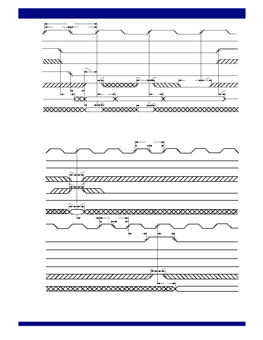
A LOW-to-HIGH transition on the
RST input loads the Almost-Full and
Almost-Empty Offset register (X) with the value selected by the Flag Select
(FS0, FS1) inputs. The values that can be loaded into the register are shown
in Table 1. For the relevant Reset timing and preset value loading timing
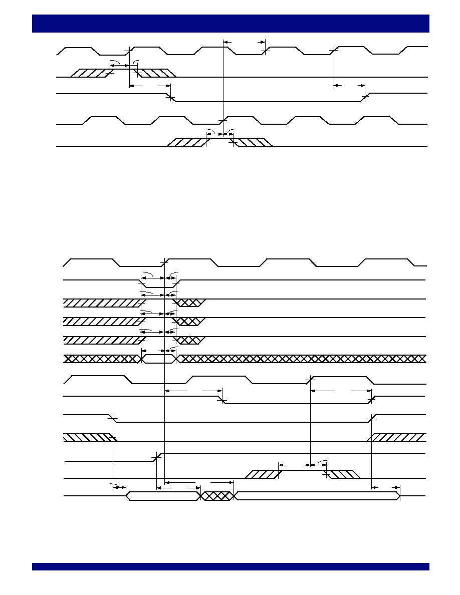
diagram, see Figure 2. The relevant Write timing diagram for Port A can be found
in Figure 3.
FIFO WRITE/READ OPERATION
The state of the port-A data (A0-A35) outputs is controlled by the port-
A Chip Select (
CSA) and the port-A Write/Read select (W/RA). The A0-A35
outputs are in the high-impedance state when either
CSA or W/RA is HIGH.
The A0-A35 outputs are active when both
CSA and W/RA are LOW. Data
is loaded into the FIFO from the A0-A35 inputs on a LOW-to-HIGH transition
of CLKA when
CSA is LOW, W/RA is HIGH, ENA is HIGH, MBA is LOW, and
FF is HIGH (see Table 2).
The port-B control signals are identical to those of port A. The state of
the port-B data (B0-B35) outputs is controlled by the port-B Chip Select
(
CSB) and the port-B Write/Read select (W/RB). The B0-B35 outputs are in
the high-impedance state when either
CSB or W/RB is HIGH. The B0-B35
outputs are active when both
CSB and W/RB are LOW. Data is read from the
FIFO to the B0-B35 outputs by a LOW-to-HIGH transition of CLKB when
CSB
is LOW, W/
RB is LOW, ENB is HIGH, MBB is LOW, and EF is HIGH (see Table
3). The relevant Read timing diagram for Port B can be found in Figure 4.
The setup and hold-time constraints to the port clocks for the port Chip
Selects (
CSA, CSB) and Write/Read selects (W/RA, W/RB) are only for enabling
write and read operations and are not related to HIGH-impedance control of
the data outputs. If a port enable is LOW during a clock cycle, the port's Chip
Select and Write/Read select can change states during the setup and hold-time
window of the cycle.
TABLE 1 ≠ FLAG PROGRAMMING
TABLE 2 ≠ PORT-A ENABLE FUNCTION TABLE
TABLE 3 ≠ PORT-B ENABLE FUNCTION TABLE

11
IDT72V3611 3.3V, CMOS SyncFIFO
TM
64 x 36
COMMERCIAL TEMPERATURE RANGE
NOTE:
1. X is the value in the Almost-Empty flag and Almost-Full flag register.
Synchronized
Synchronized
Number of Words
to CLKB
to CLKA
in the FIFO
EF
AE
AF
FF
0
L
L
H
H
1 to X
H
L
H
H
(X+1) to [64-(X+1)]
H
H
H
H
(64-X) to 63
H
H
L
H
64
H
H
L
L
A LOW-to-HIGH transition on CLKA begins the first synchronization cycle
of a read if the clock transition occurs at time t
SKEW1
or greater after the read.
Otherwise, the subsequent clock cycle can be the first synchronization cycle (see
Figure 6).
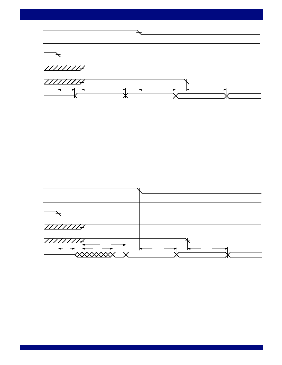
ALMOST-EMPTY FLAG (
AE )
The FIFO Almost-Empty flag is synchronized to the port clock that reads
data from its array (CLKB). The state machine that controls the
AE flag monitors
a write pointer and read pointer comparator that indicates when the FIFO
memory status is almost-empty, almost-empty+1, or almost-empty+2. The
almost-empty state is defined by the value of the Almost-Full and Almost-Empty
Offset register (X). This register is loaded with one of four preset values during
a device reset (see the Reset section). The
AE flag is LOW when the FIFO
contains X or less words in memory and is HIGH when the FIFO contains (X+1)
or more words.
Two LOW-to-HIGH transitions on the port-B clock (CLKB) are required
after a FIFO write for the
AE flag to reflect the new level of fill. Therefore, the
AE flag of a FIFO containing (X+1) or more words remains LOW if two CLKB
cycles have not elapsed since the write that filled the memory to the (X+1) level.
The
AE flag is set HIGH by the second CLKB LOW-to-HIGH transition after the
FIFO write that fills memory to the (X+1) level. A LOW-to-HIGH transition on
CLKB begins the first synchronization cycle if it occurs at time t
SKEW2
or greater
after the write that fills the FIFO to (X+1) words. Otherwise, the subsequent CLKB
cycle can be the first synchronization cycle (see Figure 7).
ALMOST-FULL FLAG (
AF )
The FIFO Almost-Full flag is synchronized to the port clock that writes
data to its array (CLKA). The state machine that controls an
AF flag monitors
a write pointer and read pointer comparator that indicates when the FIFO
memory status is almost-full, almost- full-1, or almost-full-2. The almost-full state
is defined by the value of the Almost-Full and Almost-Empty Offset register (X).
This register is loaded with one of four preset values during a device reset (see
the Reset section). The
AF flag is LOW when the FIFO contains (64-X) or more
words in memory and is HIGH when the FIFO contains [64-(X+1)] or less words.
Two LOW-to-HIGH transitions on the port-A clock (CLKA) are required
after a FIFO read for the
AF flag to reflect the new level of fill. Therefore, the
AF flag of a FIFO containing [64-(X+1)] or less words remains LOW if two CLKA
cycles have not elapsed since the read that reduced the number of words in
memory to [64-(X+1)]. The
AF flag is set HIGH by the second CLKA LOW-to-
HIGH transition after the FIFO read that reduces the number of words in memory
to [64-(X+1)]. A LOW-to-HIGH transition on CLKA begins the first synchroni-
zation cycle if it occurs at time t
SKEW2
or greater after the read that reduces the
number of words in memory to [64-(X+1)]. Otherwise, the subsequent CLKA
cycle can be the first synchronization cycle (see Figure 8).
MAILBOX REGISTERS
Two 36-bit bypass registers are on the IDT72V3611 to pass command and
control information between port A and port B. The Mailbox select (MBA, MBB)
inputs choose between a mail register and a FIFO for a port data transfer
operation. A LOW-to-HIGH transition on CLKA writes A0-A35 data to the mail1
register when port-A write is selected by
CSA, W/RA, and ENA with MBA HIGH.
A LOW-to-HIGH transition on CLKB writes B0-B35 data to the mail2 register
when port-B write is selected by
CSB, W/RB, and ENB with MBB HIGH. Writing
data to a mail register sets its corresponding flag (
MBF1 or MBF2) LOW.
Attempted writes to a mail register are ignored while its mail flag is LOW.
When the port-B data (B0-B35) outputs are active, the data on the bus
comes from the FIFO output register when the port-B Mailbox select (MBB) input
is LOW and from the mail1 register when MBB is HIGH. Mail2 data is always
SYNCHRONIZED FIFO FLAGS
Each FIFO flag is synchronized to its port clock through two flip-flop stages.
This is done to improve the flags' reliability by reducing the probability of
metastable events on their outputs when CLKA and CLKB operate asynchro-
nously to one another.
FF and AF are synchronized to CLKA. EF and AE are
synchronized to CLKB. Table 4 shows the relationship to the flags to the FIFO.
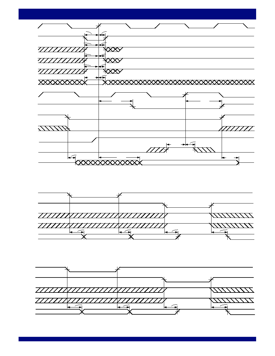
EMPTY FLAG (
EF )
The FIFO Empty Flag is synchronized to the port clock that reads data from
its array (CLKB). When the
EF is HIGH, new data can be read to the FIFO output
register. When the
EF is LOW, the FIFO is empty and attempted FIFO reads
are ignored.
The FIFO read pointer is incremented each time a new word is clocked
to its output register. The state machine that controls an
EF monitors a write
pointer and read pointer comparator that indicates when the FIFO memory
status is empty, empty+1, or empty+2. A word written to the FIFO can be read
to the FIFO output register in a minimum of three port-B clock (CLKB) cycles.
Therefore, an
EF is LOW if a word in memory is the next data to be sent to the
FIFO output register and two CLKB cycles have not elapsed since the time the
word was written. The
EF of the FIFO is set HIGH by the second LOW-to-HIGH
transition of CLKB, and the new data word can be read to the FIFO output
register in the following cycle.
A LOW-to-HIGH transition on CLKB begins the first synchronized cycle of
a write if the clock transition occurs at time t
SKEW1
or greater after the write.
Otherwise, the subsequent CLKB cycle can be the first synchronization cycle
(see Figure 5).
FULL FLAG (
FF )
The FIFO Full Flag is synchronized to the port clock that writes data to its
array (CLKA). When the
FF is HIGH, a FIFO memory location is free to receive
new data. No memory locations are free when the
FF is LOW and attempted
writes to the FIFO are ignored.
Each time a word is written to the FIFO, its write pointer is incremented. The
state machine that controls the
FF monitors a write pointer and read pointer
comparator that indicates when the FIFO memory status is full, full-1, or full-2.
From the time a word is read from the FIFO, its previous memory location is
ready to be written in a minimum of three port-A clock cycles. Therefore, a
FF
is LOW if less than two CLKA cycles have elapsed since the next memory write
location has been read. The second LOW-to-HIGH transition on CLKA after
the read sets the
FF HIGH and data can be written in the following clock cycle.
TABLE 4 ≠ FIFO FLAG OPERATION

12
IDT72V3611 3.3V, CMOS SyncFIFO
TM
64 x 36
COMMERCIAL TEMPERATURE RANGE
present on the port-A data (A0-A35) outputs when they are active. The Mail1
Register Flag (
MBF1) is set HIGH by a LOW-to-HIGH transition on CLKB when
a port-B read is selected by
CSB, W/RB, and ENB with MBB HIGH. The Mail2
Register Flag (
MBF2) is set HIGH by a LOW-to-HIGH transition on CLKA when
a port-A read is selected by
CSA, W/RA, and ENA with MBA HIGH. The data
in a mail register remains intact after it is read and changes only when new data
is written to the register. For relevant mail register and mail register flag timing
diagrams, see Figure 9 and Figure 10.
PARITY CHECKING
The port-A (A0-A35) inputs and port-B (B0-B35) inputs each have four
parity trees to check the parity of incoming (or outgoing) data. A parity failure
on one or more bytes of the input bus is reported by a LOW level on the port
Parity Error Flag (
PEFA, PEFB). Odd or even parity checking can be selected,
and the Parity Error Flags can be ignored if this feature is not desired.
Parity status is checked on each input bus according to the level of the Odd/
Even parity (ODD/
EVEN) select input. A parity error on one or more bytes
of a port is reported by a LOW level on the corresponding port Parity Error Flag
(
PEFA, PEFB) output. Port-A bytes are arranged as A0-A8, A9-A17, A18-
A26, and A27-A35, and port-B bytes are arranged as B0-B8, B9-B17, B18-
B26, and B27-B35. When Odd/Even parity is selected, a port Parity Error Flag
(
PEFA, PEFB) is LOW if any byte on the port has an odd/even number of LOW
levels applied to its bits.
The four parity trees used to check the A0-A35 inputs are shared by the
mail2 register when parity generation is selected for port-A reads
(PGA=HIGH). When port-A read from the mail2 register with parity generation
is selected with
CSA LOW, ENA HIGH, W/RA LOW, MBA HIGH, and PGA
HIGH, the port-A Parity Error Flag (
PEFA) is held HIGH regardless of the levels
applied to the A0-A35 inputs. Likewise, the parity trees used to check the B0-
B35 inputs are shared by the mail1 register when parity generation is selected
for port-B reads (PGB=HIGH). When a port-B read from the mail1 register with
parity generation is selected with
CSB LOW, ENB HIGH, W/RB LOW, MBB
HIGH, and PGB HIGH, the port-B Parity Error Flag (
PEFB) is held HIGH
regardless of the levels applied to the B0-B35 inputs.
PARITY GENERATION
A HIGH level on the port-A Parity Generate select (PGA) or port-B Parity
Generate select (PGB) enables the IDT72V3611 to generate parity bits for
port reads from a FIFO or mailbox register. Port-A bytes are arranged as A0-
A8, A9-A17, A18-A26, and A27-A35, with the most significant bit of each byte
used as the parity bit. Port-B bytes are arranged as B0-B8, B9-B17, B18-B26,
and B27-B35, with the most significant bit of each byte used as the parity bit. A
write to a FIFO or mail register stores the levels applied to all thirty-six inputs
regardless of the state of the Parity Generate select (PGA, PGB) inputs. When
data is read from a port with parity generation selected, the lower eight bits of
each byte are used to generate a parity bit according to the level on the ODD/
EVEN select. The generated parity bits are substituted for the levels originally
written to the most significant bits of each byte as the word is read to the data
outputs.
Parity bits for FIFO data are generated after the data is read from the FIFO
RAM and before the data is written to the output register. Therefore, the port-
B Parity Generate select (PGB) and ODD/
EVEN have setup and hold time
constraints to the port-B clock (CLKB) for a rising edge of CLKB used to read
a new word to the FIFO output register.
The circuit used to generate parity for the mail1 data is shared by the port-
B bus (B0-B35) to check parity and the circuit used to generate parity for the
mail2 data is shared by the port-A bus (A0-A35) to check parity. The shared
parity trees of a port are used to generate parity bits for the data in a mail register
when the port Write/Read select (W/
RA, W/RB) input is LOW, the port Mail select
(MBA, MBB) input is HIGH, Chip Select (
CSA, CSB) is LOW, Enable (ENA,
ENB) is HIGH, and the port Parity Generate select (PGA, PGB) is HIGH.
Generating parity for mail register data does not change the contents of the
register (see Figure 13 and Figure 14).

13
IDT72V3611 3.3V, CMOS SyncFIFO
TM
64 x 36
COMMERCIAL TEMPERATURE RANGE
Figure 3. FIFO Write Cycle Timing
Figure 2. Device Reset and Loading the X Register with the Value of Eight
CLKA
RST
FF
AE
AF
MBF1,
MBF2
CLKB
EF
FS1,FS0
4657 drw 05
t
RSTS
t
RSTH
t
FSH
t
FSS
t
WFF
t
WFF
t
PAE
0,1
t
PAF
t
RSF
t
REF
CLKA
FF
ENA
MBA
CSA
W/
RA
t
CLKH
t
CLKL
t
CLK
t
ENS1
t
ENS1
t
ENS3
t
ENS2
t
ENH1
t
ENH1
t
ENH3
t
ENH2
t
ENS2
t
ENH2
t
ENH2
t
ENS2
4657 drw 06
PEFA
A0 - A35
t
DS
t
DH
W1
W2
No Operation
ODD/
EVEN
Valid
Valid
t
PDPE
t
PDPE
HIGH
14
IDT72V3611 3.3V, CMOS SyncFIFO
TM
64 x 36
COMMERCIAL TEMPERATURE RANGE
Figure 5.
EF
Flag Timing and First Data Read when the FIFO is Empty
NOTE:
1. t
SKEW1
is the minimum time between a rising CLKA edge and a rising CLKB edge for
EF to transition HIGH in the next CLKB cycle. If the time between the rising CLKA edge and rising
CLKB edge is less than t
SKEW1
, then the transition of
EF HIGH may occur one CLKB cycle later than shown.
Figure 4. FIFO Read Cycle Timing
4657 drw 07
CLKB
EF
ENB
B0 - B35
MBB
CSB
W/
RB
t
CLK
t
CLKH
t
CLKL
t
ENS2
t
MDV
t
EN
t
A
t
A
t
ENH2
t
ENS2
t
ENH2
t
ENS2
t
ENH2
t
DIS
No Operation
HIGH
PGB,
ODD/
EVEN
Previous Data
Word 1
Word 2
t
PGS
t
PGH
t
PGS
t
PGH
CSA
W
RA
MBA
FFA
A0 - A35
CLKB
EF
CSB
W/
RB
MBB
ENA
CLKA
1
2
4657 drw 08
t
CLKH
t
CLKL
t
CLK
t
ENS3
t
ENS2
t
ENH3
t
ENH2
t
DS
t
DH
t
SKEW1
t
CLK
t
CLKL
t
REF
t
REF
t
ENS2
t
ENH2
t
A
W1
Empty FIFO
LOW
HIGH
LOW
LOW
LOW
t
CLKH
W1
HIGH
(1)
ENB
B0 - B35
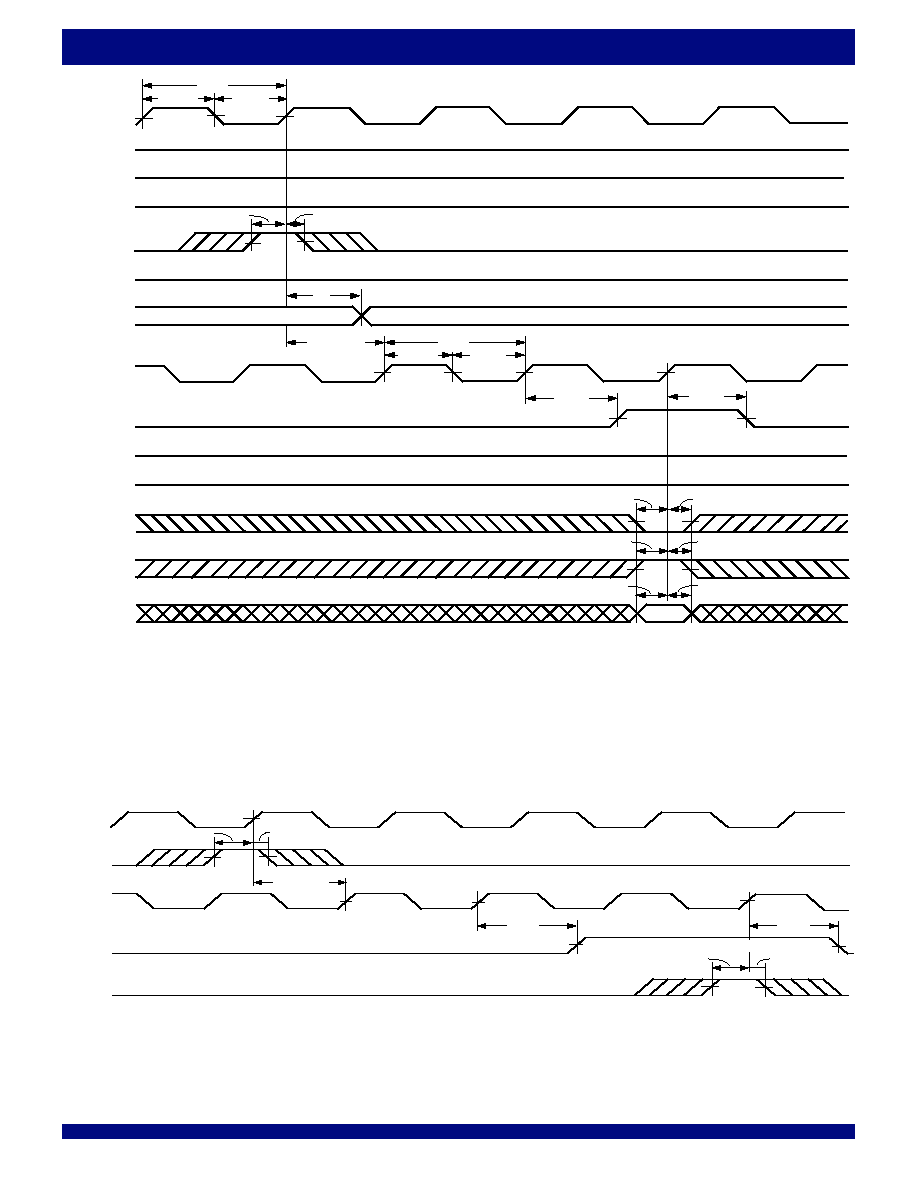
15
IDT72V3611 3.3V, CMOS SyncFIFO
TM
64 x 36
COMMERCIAL TEMPERATURE RANGE
Figure 7. Timing for
AE
when the FIFO is Almost-Empty
NOTES:
1. t
SKEW2
is the minimum time between a rising CLKA edge and a rising CLKB edge for
AE to transition HIGH in the next CLKB cycle. If the time between the rising CLKA edge and
rising CLKB edge is less than t
SKEW2
, then
AE may transition HIGH one CLKB cycle later than shown.
2. FIFO write (
CSA = L, W/RA = H, MBA = L), FIFO read (CSB = L, W/RB = L, MBB = L).
NOTE:
1. t
SKEW1
is the minimum time between a rising CLKB edge and a rising CLKA edge for
FF to transition HIGH in the next CLKA cycle. If the time between the rising CLKB edge and rising
CLKA edge is less than t
SKEW1
, then the transition of
FF HIGH may occur one CLKA cycle later than shown.
Figure 6.
FF
Flag Timing and First Available Write when the FIFO is Full
CSB
EFB
W/
RB
MBB
ENB
B0 -B35
CLKB
FF
CLKA
CSA
4657 drw 09
W
RA
1
2
A0 - A35
MBA
ENA
t
CLK
t
CLKH
t
CLKL
t
ENS2
t
ENH2
t
A
t
SKEW1
(1)
t
CLK
t
CLKH
t
CLKL
t
WFF
t
ENS3
t
ENS2
t
DS
t
ENH2
t
DH
To FIFO
Previous Word in FIFO Output Register
Next Word From FIFO
LOW
LOW
LOW
HIGH
LOW
HIGH
FIFO Full
t
WFF
t
ENH3
AE
CLKA
ENB
4657 drw 10
ENA
CLKB
2
1
t
ENS2
t
ENH2
t
SKEW2
(1)
t
PAE
t
PAE
t
ENS2
t
ENH2
X Word in FIFO
(X+1) Words in FIFO
16
IDT72V3611 3.3V, CMOS SyncFIFO
TM
64 x 36
COMMERCIAL TEMPERATURE RANGE
Figure 8. Timing for
AF
when the FIFO is Almost-Full
Figure 9. Timing for Mail1 Register and
MBF1
Flag
NOTES:
1. t
SKEW2
is the minimum time between a rising CLKA edge and a rising CLKB edge for
AF to transition HIGH in the next CLKA cycle. If the time between the rising CLKA edge and
rising CLKB edge is less than t
SKEW2
, then
AF may transition HIGH one CLKA cycle later than shown.
2. FIFO write (
CSA = L, W/RA = H, MBA = L), FIFO read (CSB = L, W/RB = L, MBB = L).
NOTE:
1. Port-B parity generation off (PGB = L)
AF
CLKA
ENB
4657 drw 11
ENA
CLKB
1
2
t
SKEW2
(1)
t
ENS2
t
ENH2
t
PAF
t
ENS2
t
ENH2
t
PAF
[64-(X+1)] Words in FIFO
(64-X) Words in FIFO
4657 drw 12
CLKA
ENA
A0 - A35
MBA
CSA
W/
RA
CLKB
MBF1
CSB
MBB
ENB
B0 - B35
W/
RB
W1
t
ENS1
t
ENH1
t
DS
t
DH
t
PMF
t
PMF
t
EN
t
MDV
t
PMR
t
ENS2
t
ENH2
t
DIS
W1 (Remains valid in Mail1 Register after read)
FIFO Output Register
t
ENS1
t
ENH1
t
ENS1
t
ENH1
t
ENS1
t
ENH1
17
IDT72V3611 3.3V, CMOS SyncFIFO
TM
64 x 36
COMMERCIAL TEMPERATURE RANGE
Figure 11. ODD/
EVEN
, W/RA, MBA, and PGA to
PEFA
Timing
NOTE:
1.
CSA = L and ENA = H.
Figure 12. ODD/
EVEN
, W/RB, MBB, and PGB to
PEFB
Timing
4657 drw 13
CLKB
ENB
B0 - B35
MBB
CSB
W/
RB
CLKA
MBF2
CSA
MBA
ENA
A0 - A35
W/
RA
W1
t
ENS1
t
ENH1
t
DS
t
DH
t
PMF
t
PMF
t
EN
t
PMR
t
ENS2
t
ENH2
t
DIS
W1 (Remains valid in Mail2 Register after read)
t
ENS1
t
ENH1
t
ENS1
t
ENH1
t
ENS1
t
ENH1
4657 drw 14
ODD/
EVEN
PEFA
PGA
MBA
W/
RA
Valid
Valid
Valid
Valid
t
POPE
t
PEPE
t
POPE
t
PEPE
4657 drw 15
ODD/
EVEN
PEFB
PGB
MBB
W/
RB
Valid
Valid
Valid
Valid
t
POPE
t
PEPE
t
POPE
t
PEPE
Figure 10. Timing for Mail2 Register and
MBF2
Flag
NOTE:
1. Port-A parity generation off (PGA = L)
NOTE:
1.
CSB = L and ENB = H.
18
IDT72V3611 3.3V, CMOS SyncFIFO
TM
64 x 36
COMMERCIAL TEMPERATURE RANGE
Figure 14. Parity Generation Timing when reading from the Mail1 Register
Figure 13. Parity Generation Timing when reading from the Mail2 Register
NOTE:
1. ENA = H.
NOTE:
1. ENB = H.
4657 drw 16
ODD/
EVEN
A8, A17,
A26, A35
PGA
MBA
W/
RA
Mail2 Data
Generated Parity
Generated Parity
Mail2 Data
CSA
LOW
t
EN
t
PEPB
t
POPB
t
PEPB
4657 drw 17
ODD/
EVEN
B8, B17,
B26, B35
PGB
MBB
W/
RB
Mail1
Data
Generated Parity
Generated Parity
Mail1 Data
CSB
LOW
t
EN
t
PEPB
t
POPB
t
PEPB
t
MDV

19
IDT72V3611 3.3V, CMOS SyncFIFO
TM
64 x 36
COMMERCIAL TEMPERATURE RANGE
NOTE:
1. Includes probe and jig capacitance.
Figure 15. Load Circuit and Voltage Waveforms
4657 drw 18
PARAMETER MEASUREMENT INFORMATION
From Output
Under Test
30 pF
330
3.3V
510
PROPAGATION DELAY
LOAD CIRCUIT
3 V
GND
Timing
Input
Data,
Enable
Input
GND
3 V
1.5 V
1.5 V
VOLTAGE WAVEFORMS
SETUP AND HOLD TIMES
VOLTAGE WAVEFORMS
PULSE DURATIONS
VOLTAGE WAVEFORMS
ENABLE AND DISABLE TIMES
VOLTAGE WAVEFORMS
PROPAGATION DELAY TIMES
3 V
GND
GND
3 V
1.5 V
1.5 V
1.5 V
1.5 V
t
W
Output
Enable
Low-Level
Output
High-Level
Output
3 V
OL
GND
3 V
1.5 V
1.5 V
1.5 V
1.5 V
Ø
OH
OV
Ø
GND
OH
OL
1.5 V
1.5 V
1.5 V
1.5 V
Input
In-Phase
Output
High-Level
Input
Low-Level
Input
V
V
V
V
1.5 V
3 V
t
S
t
h
t
PLZ
t
PHZ
t
PZL
t
PZH
t
PD
t
PD
(1)

CORPORATE HEADQUARTERS
for SALES:
for Tech Support:
2975 Stender Way
800-345-7015 or 408-727-6116
408-330-1753
Santa Clara, CA 95054
fax: 408-492-8674
email: FIFOhelp@idt.com
www.idt.com
20
ORDERING INFORMATION
BLANK
PF
PQF
15
20
L
72V3611
4657 drw 19
Commercial (0
∞C to +70∞C)
Thin Quad Flat Pack (TQFP, PN120-1)
Plastic Quad Flat Pack (PQFP, PQ132-1)
Low Power
64 x 36
3.3V SyncFIFO
XXXXXX
IDT
Device Type
X
XX
X
X
Power
Speed
Package
Process/
Temperature
Range
Clock Cycle Time (t
CLK
)
Speed in Nanoseconds
Commercial Only
NOTE:
1. Industrial temperature range is available by special order.
DATASHEET DOCUMENT HISTORY
07/10/2000
pg. 1
05/27/2003
pg. 6.