 | –≠–ª–µ–∫—Ç—Ä–æ–Ω–Ω—ã–π –∫–æ–º–ø–æ–Ω–µ–Ω—Ç: 72V3626 | –°–∫–∞—á–∞—Ç—å:  PDF PDF  ZIP ZIP |
2001 Integrated Device Technology, Inc. All right reserved. Product specifications subject to change without notice.
DSC-4665/4
AUGUST 2001
3.3 VOLT CMOS TRIPLE BUS
SyncFIFO
TM
WITH BUS-MATCHING
256 x 36 x 2, 512 x 36 x 2,
1,024 x 36 x 2
IDT72V3626
IDT72V3636
IDT72V3646
1
IDT, the IDT logo are registered trademarks of Integrated Device Technology, Inc. SyncFIFO is a trademark of Integrated Device Technology, Inc.
COMMERCIAL TEMPERATURE RANGE
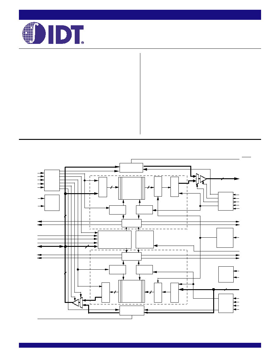
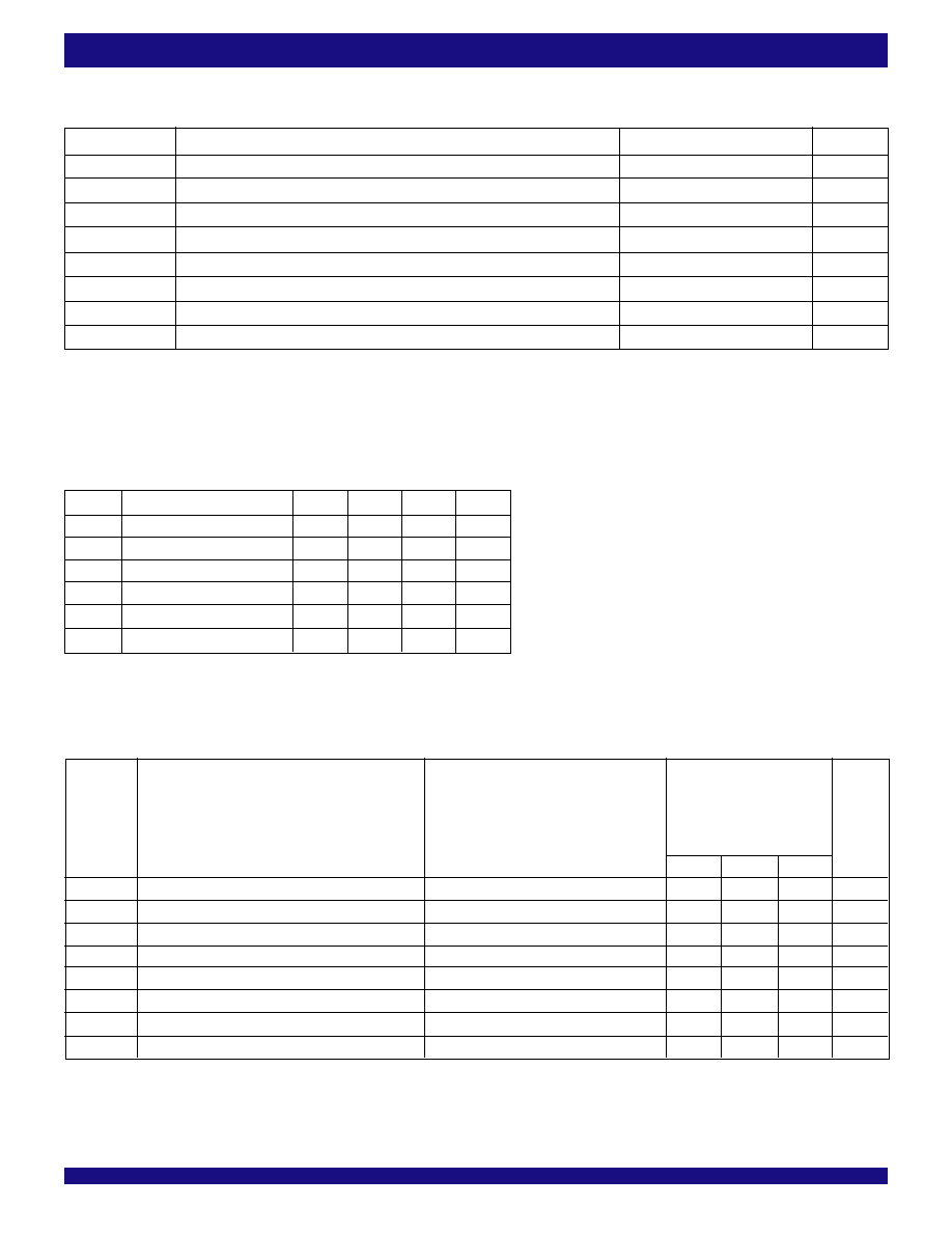
.UNCTIONAL BLOCK DIAGRAM
.EATURES:
∑
∑
∑
∑
∑
Memory storage capacity:
IDT72V3626≠256 x 36 x 2
IDT72V3636≠512 x 36 x 2
IDT72V3646≠1,024 x 36 x 2
∑
∑
∑
∑
∑
Clock frequencies up to 100 MHz (6.5ns access time)
∑
∑
∑
∑
∑
Two independent FIFOs buffer data between one bidirectional
36-bit port and two unidirectional 18-bit ports (Port C receives
and Port B transmits)
∑
∑
∑
∑
∑
18-bit (word) and 9-bit (byte) bus sizing of 18 bits (word) on
Ports B and C
∑
∑
∑
∑
∑
Select IDT Standard timing (using
EFA, EFB, FFA, and FFC flag
functions) or First Word Fall Through Timing (using ORA, ORB,
IRA, and IRC flag functions)
∑
∑
∑
∑
∑
Programmable Almost-Empty and Almost-Full flags; each has
three default offsets (8, 16 and 64)
∑
∑
∑
∑
∑
Serial or parallel programming of partial flags
∑
∑
∑
∑
∑
Big- or Little-Endian format for word and byte bus sizes
∑
∑
∑
∑
∑
Master Reset clears data and configures FIFO, Partial Reset
clears data but retains configuration settings
∑
∑
∑
∑
∑
Mailbox bypass registers for each FIFO
∑
∑
∑
∑
∑
Free-running CLKA, CLKB and CLKC may be asynchronous or
coincident (simultaneous reading and writing of data on a single
clock edge is permitted)
∑
∑
∑
∑
∑
Auto power down minimizes power dissipation
∑
∑
∑
∑
∑
Available in a space-saving 128-pin Thin Quad Flatpack (TQFP)
∑
∑
∑
∑
∑
Pin and functionally compatible versions of 5V operating
IDT723626/723636/723646
∑
∑
∑
∑
∑
Industrial temperature range (≠40
∞∞
∞∞
∞
C to +85
∞∞
∞∞
∞
C) is available
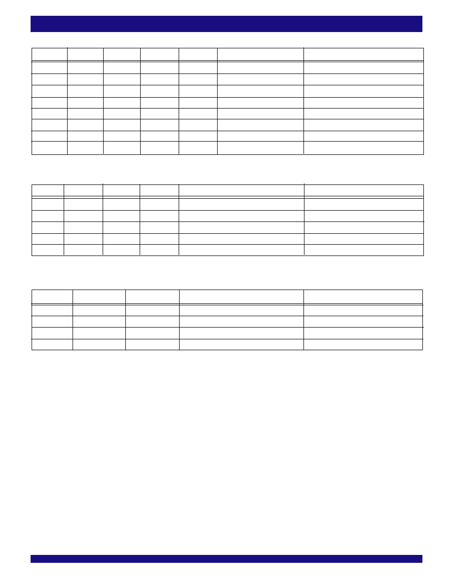
Mail 1
Register
Programmable Flag
Offset Registers
Input
Register
RAM ARRAY
256 x 36
512 x 36
1,024 x 36
Write
Pointer
Read
Pointer
Status Flag
Logic
Input
Register
Output
Register
RAM ARRAY
256 x 36
512 x 36
1,024 x 36
Write
Pointer
Read
Pointer
Status Flag
Logic
CLKA
CSA
W/
R
A
ENA
MBA
Port-A
Control
Logic
FIFO1,
Mail1
Reset
Logic
MRS1
Mail 2
Register
MBF2
WENC
Port-C
Control
Logic
FIFO2,
Mail2
Reset
Logic
MRS2
MBF1
FIFO1
FIFO2
10
EFB
/ORB
AEB
18
18
FFC
/IRC
AFC
B
0
-B
17
FFA
/IRA
AFA
SPM
FS0/SD
FS1/
SEN
A
0
-A
35
EFA
/ORA
AEA
4665 drw01
36
36
Output Bus-
Matching
Output
Register
PRS2
PRS1
Timing
Mode
FWFT
C
0
-C
17
CLKB
RENB
CSB
MBB
Port-B
Control
Logic
Common
Port
Control
Logic
(B and C)
BE
SIZEB
SIZEC
CLKC
MBC
36
36
36
36
Input Bus-
Matching
2
COMMERCIAL TEMPERATURE RANGE
IDT72V3626/72V3636/72V3646 CMOS 3.3V TRIPLE BUS SyncFIFO
TM
WITH BUS-MATCHING 256 x 36 x 2, 512 x 36 x 2, 1,024 x 36 x 2
FIFOs on board each chip buffer data between a bidirectional 36-bit bus (Port
A) and two unidirectional 18-bit buses (Port B transmits data, Port C receives
data.) FIFO data can be read out of Port B and written into Port C using either
18-bit or 9-bit formats with a choice of Big- or Little-Endian configurations.
These devices are a synchronous (clocked) FIFO, meaning each port
employs a synchronous interface. All data transfers through a port are gated
to the LOW-to-HIGH transition of a port clock by enable signals. The clocks for
DESCRIPTION:
The IDT72V3626/72V3636/72V3646 are pin and functionally compatible
versions of the IDT723626/723636/723646, designed to run off a 3.3V supply
for exceptionally low-power consumption. These devices are a monolithic,
high-speed, low-power, CMOS Triple Bus synchronous (clocked) FIFO
memory which supports clock frequencies up to 100 MHz and has read access
times as fast as 6.5ns. Two independent 256/512/1,024 x 36 dual-port SRAM
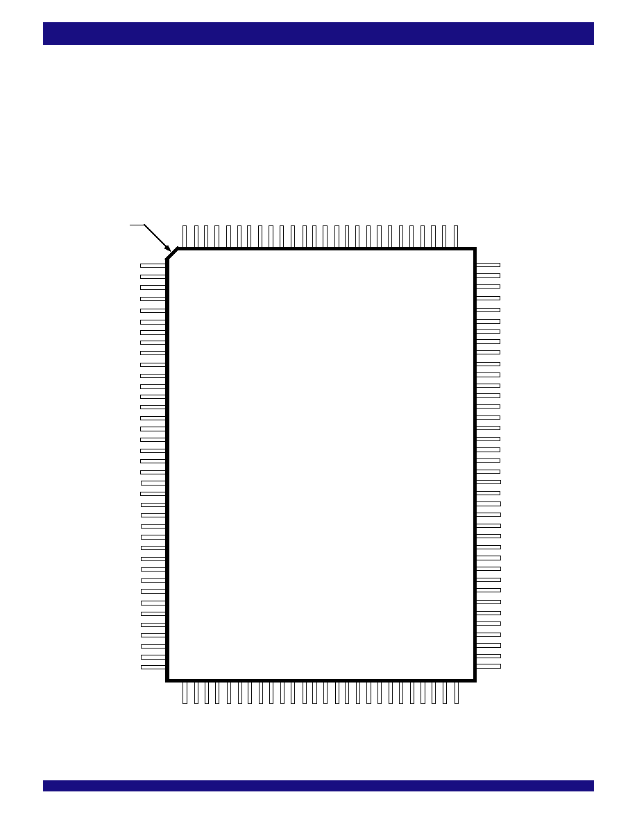
PIN CON.IGURATION
TQFP (PK128-1, order code: PF)
TOP VIEW
W/
RA
CLKB
4665 drw 02
1
2
3
4
5
6
7
8
9
10
11
12
13
14
15
16
17
18
19
20
21
22
23
24
25
26
27
28
29
30
31
32
33
34
35
36
37
38
ENA
CLKA
GND
A35
A34
A33
A32
Vcc
A31
A30
GND
A29
A28
A27
A26
A25
A24
A23
BE/
FWFT
GND
A22
Vcc
A21
A20
A19
A18
GND
A17
A16
A15
A14
A13
Vcc
A12
GND
A11
A10
39
40
41
42
43
44
45
46
47
48
49
50
51
52
53
54
55
56
57
58
59
60
61
62
63
64
65
66
67
68
69
70
71
72
73
74
75
76
77
78
79
80
81
82
83
84
85
86
87
88
89
90
91
92
93
94
95
96
97
98
99
100
102
101
128
127
126
125
124
123
122
121
120
119
118
117
116
115
114
113
112
111
110
109
108
107
106
105
PRS2
C17
C16
C15
C14
MBC
GND
C13
C12
C11
C10
C9
C8
C7
C6
SIZEB
GND
C5
C4
C3
C2
C1
C0
GND
B17
B16
B15
B14
B13
B12
GND
B11
B10
CSA
FFA
/IRA
EFA
/ORA
PRS1
AFA
AEA
MBF2
MBA
MRS1
FS0/SD
CLKC
GND
FS1/
SEN
MRS2
MBB
MBF1
AEB
AFC
EFB
/ORB
FFC
/IRC
GND
CSB
WENC
RENB
A9
A8
A7
A
6
GND
A
5
A4
A3
SPM
A2
A1
A0
GND
B0
B1
B2
B3
B
4
B
5
GND
B
6
B7
B
9
104
103
INDEX
SIZEC
B8
V
CC
V
CC
V
CC
V
CC
V
CC
V
CC
V
CC

3
IDT72V3626/72V3636/72V3646 CMOS 3.3V Triple Bus SyncFIFO
TM
with Bus-Matching 256x36x2, 512x36x2, 1,024x36x2
COMMERCIAL TEMPERATURE RANGE
IDT72V3626/72V3636/72V3646 CMOS 3.3V TRIPLE BUS SyncFIFO
TM
WITH BUS-MATCHING 256 x 36 x 2, 512 x 36 x 2, 1,024 x 36 x 2
each port are independent of one another and can be asynchronous or
coincident. The enables for each port are arranged to provide a simple
bidirectional interface between microprocessors and/or buses with synchro-
nous control.
Communication between each port may bypass the FIFOs via two mailbox
registers. The mailbox registers' width matches the selected bus width of ports
B and C. Each mailbox register has a flag (
MBF1 and MBF2) to signal when
new mail has been stored.
Two kinds of reset are available on these FIFOs: Master Reset and Partial
Reset. Master Reset initializes the read and write pointers to the first location
of the memory array and selects serial flag programming, parallel flag program-
ming, or one of three possible default flag offset settings, 8, 16 or 64. Each FIFO
has its own, independent Master Reset pin,
MRS1 and MRS2.
Partial Reset also sets the read and write pointers to the first location of the
memory. Unlike Master Reset, any settings existing prior to Partial Reset (i.e.,
programming method and partial flag default offsets) are retained. Partial Reset
is useful since it permits flushing of the FIFO memory without changing any
configuration settings. Each FIFO has its own, independent Partial Reset pin,
PRS1 and PRS2.
These devices have two modes of operation: In the IDT Standard mode,
the first word written to an empty FIFO is deposited into the memory array. A
read operation is required to access that word (along with all other words
residing in memory). In the First Word Fall Through mode (FWFT), the first
word written to an empty FIFO appears automatically on the outputs, no read
operation required (Nevertheless, accessing subsequent words does neces-
sitate a formal read request). The state of the BE/
FWFT pin during Master Reset
determines the mode in use.
Each FIFO has a combined Empty/Output Ready Flag (
EFA/ORA and
EFB/ORB) and a combined Full/Input Ready Flag (FFA/IRA and FFC/IRC).
The
EF and FF functions are selected in the IDT Standard mode. EF indicates
whether or not the FIFO memory is empty.
FF shows whether the memory is
full or not. The IR and OR functions are selected in the First Word Fall Through
mode. IR indicates whether or not the FIFO has available memory locations.
OR shows whether the FIFO has data available for reading or not. It marks the
presence of valid data on the outputs.
Each FIFO has a programmable Almost-Empty flag (
AEA and AEB) and
a programmable Almost-Full flag (
AFA and AFC). AEA and AEB indicate when
a selected number of words remain in the FIFO memory.
AFA and AFC indicate
when the FIFO contains more than a selected number of words.
FFA/IRA, FFC/IRC, AFA and AFC are two-stage synchronized to the
Port Clock that writes data into its array.
EFA/ORA, EFB/ORB, AEA, and AEB
are two-stage synchronized to the Port Clock that reads data from its array.
Programmable offsets for
AEA, AEB, AFA, AFC are loaded in parallel using
Port A or in serial via the SD input. The Serial Programming Mode pin (
SPM)
makes this selection. Three default offset settings are also provided. The
AEA
and
AEB threshold can be set at 8, 16 or 64 locations from the empty boundary
and the
AFA and AFC threshold can be set at 8, 16 or 64 locations from the full
boundary. All these choices are made using the FS0 and FS1 inputs during
Master Reset.
Two or more FIFOs may be used in parallel to create wider data paths.
Such a width expansion requires no additional, external components. Further-
more, two IDT72V3626/72V3636/72V3646 FIFOs can be combined with
unidirectional FIFOs capable of First Word Fall Through timing (i.e. the
SuperSync FIFO family) to form a depth expansion.
If, at any time, the FIFO is not actively performing a function, the chip will
automatically power down. During the power down state, supply current
consumption (I
CC
) is at a minimum. Initiating any operation (by activating control
inputs) will immediately take the device out of the power down state.
The IDT72V3626/72V3636/72V3646 are characterized for operation from
0
∞
C to 70
∞
C. Industrial temperature range (-40
∞
C to +85
∞
C) is available by
special order. They are fabricated using IDT's high speed, submicron CMOS
technology.
4
COMMERCIAL TEMPERATURE RANGE
IDT72V3626/72V3636/72V3646 CMOS 3.3V TRIPLE BUS SyncFIFO
TM
WITH BUS-MATCHING 256 x 36 x 2, 512 x 36 x 2, 1,024 x 36 x 2
PIN DESCRIPTIONS
Symbol
Name
I/O
Description
A0-A35
Port A Data
I/O
36-bit bidirectional data port for side A.
AEA
Port A Almost-
O
Programmable Almost-Empty flag synchronized to CLKA. It is LOW when the number of words in FIFO2
Empty Flag
is less than or equal to the value in the Almost-Empty A Offset register, X2.
AEB
Port B Almost-
O
Programmable Almost-Empty flag synchronized to CLKB. It is LOW when the number of words in FIFO1
Empty Flag
is less than or equal to the value in the Almost-Empty B Offset register, X1.
AFA
Port A Almost-
O
Programmable Almost-Full flag synchronized to CLKA. It is LOW when the number of empty locations
Full Flag
in FIFO1 is less than or equal to the value in the Almost-Full A Offset register, Y1.
AFC
Port C Almost-
O
Programmable Almost-Full flag synchronized to CLKC. It is LOW when the number of empty locations
Full Flag
in FIFO2 is less than or equal to the value in the Almost-Full C Offset register, Y2.
B0-B17
Port B Data
O
18-bit output data port for side B.
BE/
FWFT
Big-Endian/
I
This is a dual purpose pin. During Master Reset, a HIGH on BE will select Big-Endian operation.
First Word Fall
In this case, depending on the bus size, the most significant byte or word on Port A is read from
Through Select
Port B first (A-to-B data flow) or is written to Port C first (C-to-A data flow). A LOW on BE will select
Little-Endian operation. In this case, the least significant byte or word on Port A is read from Port B first
(A-to-B data flow) or is written to Port C first (C-to-A data flow).
After Master Reset, this pin selects the timing mode. A HIGH on
FWFT selects IDT Standard mode, a
LOW selects First Word Fall Through mode. Once the timing mode has been selected, the level on
FWFT must be static throughout device operation.
C0-C17
Port C Data
I
18-bit input data port for side C.
CLKA
Port A Clock
I
CLKA is a continuous clock that synchronizes all data transfers through Port A and can be
asynchronous or coincident to CLKB.
FFA/IRA, EFA/ORA, AFA, and AEA are all synchronized to
the LOW-to-HIGH transition of CLKA.
CLKB
Port B Clock
I
CLKB is a continuous clock that synchronizes all data transfers through Port B and can be asynchronous
or coincident to CLKA.
EFB/ORB and AEB are synchronized to the LOW-to-HIGH transition of CLKB.
CLKC
Port C Clock
I
CLKC is a continuous clock that synchronizes all data transfers through Port C and can be asynchronous
or coincident to CLKA.
FFC/IRC and AFC are synchronized to the LOW-to-HIGH transition of CLKC.
CSA
Port A Chip
I
CSA must be LOW to enable to LOW-to-HIGH transition of CLKA to read or write on Port A. The A0-A35
Select
outputs are in the high-impedance state when
CSA is HIGH.
CSB
Port B Chip
I
CSB must be LOW to enable a LOW-to-HIGH transition of CLKB to read data on Port B. The B0-B17
Select
outputs are in the high-impedance state when
CSB is HIGH.
EFA/ORA
Port A Empty/
O
This is a dual function pin. In the IDT Standard mode, the
EFA function is selected. EFA indicates
Output Ready
whether or not the FIFO2 memory is empty. In the FWFT mode, the ORA function is selected. ORA
Flag
indicates the presence of valid data on the A0-A35 outputs, available for reading.
EFA/ORA is
synchronized to the LOW-to-HIGH transition of CLKA.
EFB/ORB
Port B Empty/
O
This is a dual function pin. In the IDT Standard mode, the
EFB function is selected. EFB indicates
Output Ready Flag
whether or not the FIFO1 memory is empty. In the FWFT mode, the ORB function is selected. ORB
indicates the presence of valid data on the B0-B17 outputs, available for reading.
EFB/ORB is synchronized
to the LOW-to-HIGH transition of CLKB.
ENA
Port A Enable
I
ENA must be HIGH to enable a LOW-to-HIGH transition of CLKA to read or write data on Port A.
FFA/IRA
Port A Full/
O
This is a dual function pin. In the IDT Standard mode, the
FFA function is selected. FFA indicates
Input Ready Flag
whether or not the FIFO1 memory is full. In the FWFT mode, the IRA function is selected. IRA
indicates whether or not there is space available for writing to the FIFO1 memory.
FFA/IRA is
synchronized to the LOW-to-HIGH transition of CLKA.
FFC/IRC
Port C Full/
O
This is a dual function pin. In the IDT Standard mode, the
FFC function is selected. FFC indicates
Input Ready Flag
whether or not the FIFO2 memory is full. In the FWFT mode, the IRC function is selected. IRC
indicates whether or not there is space available for writing to the FIFO2 memory.
FFC/IRC is
synchronized to the LOW-to-HIGH transition of CLKC.
5
IDT72V3626/72V3636/72V3646 CMOS 3.3V Triple Bus SyncFIFO
TM
with Bus-Matching 256x36x2, 512x36x2, 1,024x36x2
COMMERCIAL TEMPERATURE RANGE
IDT72V3626/72V3636/72V3646 CMOS 3.3V TRIPLE BUS SyncFIFO
TM
WITH BUS-MATCHING 256 x 36 x 2, 512 x 36 x 2, 1,024 x 36 x 2
PIN DESCRIPTIONS (Continued)
Symbol
Name
I/O
Description
FS1/
SEN Flag Offset Select 1/
I
FS1/
SEN and FS0/SD are dual-purpose inputs used for flag Offset register programming. During Master Reset,
Serial Enable,
FS1/
SEN and FS0/SD, together with SPM, select the flag offset programming method. Three Offset register
programming methods are available: automatically load one of three preset values (8, 16, or 64), parallel
FS0/SD
Flag Offset Select 0/
load from Port A, and serial load.
Serial Data
When serial load is selected for flag Offset register programming, FS1/
SEN is used as an enable synchronous to
the LOW-to-HIGH transition of CLKA. When FS1/
SEN is LOW, a rising edge on CLKA load the bit present on
FS0/SD into the X and Y registers. The number of bit writes required to program the Offset registers is 32 for the
72V3626, 36 for the 72V3636, and 40 for the 72V3646. The first bit write stores the Y-register (Y1) MSB and the
last bit write stores the X-register (X2) LSB.
MBA
Port A Mailbox
I
A HIGH level on MBA chooses a mailbox register for a Port A read or write operation. When the A0-A35
Select
outputs are active, a HIGH level on MBA selects data from the mail2 register for output and a LOW level selects
FIFO2 output-register data for output.
MBB
Port B Mailbox
I
A HIGH level on MBB chooses a mailbox register for a Port B read operation. When the B0-B17 outputs are
Select
active, a HIGH level on MBB selects data from the mail1 register for output and a LOW level selects FIFO1 output
register data for output.
MBC
Port C Mailbox
I
A HIGH level on MBC chooses the mail2 register for a Port C write operation. This pin must be HIGH during
Select
Master Reset.
MBF1
Mail1 Register
O
MBF1 is set LOW by a LOW-to-HIGH transition of CLKA that writes data to the mail1 register. Writes to the mail1
Flag
register are inhibited while
MBF1 is LOW. MBF1 is set HIGH by a LOW-to-HIGH transition of CLKB when a
Port B read is selected and MBB is HIGH.
MBF1 is set HIGH following either a Master or Partial Reset of FIFO1.
MBF2
Mail2 Register
O
MBF2 is set LOW by a LOW-to-HIGH transition of CLKC that writes data to the mail2 register. Writes to the mail2
Flag
register are inhibited while
MBF2 is LOW. MBF2 is set HIGH by a LOW-to-HIGH transition of CLKA when a
Port A read is selected and MBA is HIGH.
MBF2 is set HIGH following either a Master or Partial Reset of FIFO2.
MRS1
Master Reset
I
A LOW on this pin initializes the FIFO1 read and write pointers to the first location of memory and sets the Port B
output register to all zeroes. A LOW-to-HIGH transition on
MRS1 selects the programming method (serial or
parallel) and one of three programmable flag default offsets for FIFO1 and FIFO2. It also configures ports B and
C for bus size and endian arrangement. Four LOW-to-HIGH transitions of CLKA and four LOW-to-HIGH
transitions of CLKB must occur while
MRS1 is LOW.
MRS2
Master Reset
I
A LOW on this pin initializes the FIFO2 read and write pointers to the first location of memory and sets the Port A
output register to all zeroes. A LOW-to-HIGH transition on
MRS2, toggled simultaneously with MRS1, selects
the programming method (serial or parallel) and one of the three flag default offsets for FIFO2. Four LOW-to-HIGH
transitions of CLKA and four LOW-to-HIGH transitions of CLKC must occur while
MRS2 is LOW.
PRS1
Partial Reset
I
A LOW on this pin initializes the FIFO1 read and write pointers to the first location of memory and sets thePort B
output register to all zeroes. During Partial Reset, the currently selected bus size, endian arrangement,
programming method (serial or parallel), and programmable flag settings are all retained.
PRS2
Partial Reset
I
A LOW on this pin initializes the FIFO2 read and write pointers to the first location of memory and sets thePort A
output register to all zeroes. During Partial Reset, the currently selected bus size, endian arrangement,
programming method (serial or parallel), and programmable flag settings are all retained.
RENB
Port B Read Enable
I
RENB must be HIGH to enable a LOW-to-HIGH transition of CLKB to read data on Port B.
SIZEB
Port B
I
SIZEB determines the bus width of Port B. A HIGH on this pin selects byte (9-bit) bus size. A LOW on this pin
Bus Size Select
selects word (18-bit) bus size. SIZEB works with SIZEC and BE to select the bus size and endian arrangement
for ports B and C. The level of SIZEB must be static throughout device operation.
SIZEC
Port C
I
SIZEC determines the bus width of Port C. A HIGH on this pin selects byte (9-bit) bus size. A LOW on this pin
Bus Size Select
selects word (18-bit) bus size. SIZEC works with SIZEB and BE to select the bus size and endian arrangement
for ports B and C. The level of SIZEC must be static throughout device operation.
SPM
Serial Programming
I
A LOW on this pin selects serial programming of partial flag offsets. A HIGH on this pin selects parallel
Mode
programming or default offsets (8, 16, or 64).
WENC
Port C Write Enable
I
WENC must be HIGH to enable a LOW-to-HIGH transition of CLKC to write data on Port C.
W/
RA
Port A Write/
I
A HIGH selects a write operation and a LOW selects a read operation on Port A for a LOW-to-HIGH transition of
Read Select
CLKA. The A0-A35 outputs are in the HIGH impedance state when W/
RA is HIGH.
6
COMMERCIAL TEMPERATURE RANGE
IDT72V3626/72V3636/72V3646 CMOS 3.3V TRIPLE BUS SyncFIFO
TM
WITH BUS-MATCHING 256 x 36 x 2, 512 x 36 x 2, 1,024 x 36 x 2
Symbol
Rating
Commercial
Unit
V
CC
Supply Voltage Range
≠0.5 to +4.6
V
V
I
(2)
Input Voltage Range
≠0.5 to V
CC
+0.5
V
V
O
(2)
Output Voltage Range
≠0.5 to V
CC
+0.5
V
I
IK
Input Clamp Current (V
I
< 0 or V
I
> V
CC
)
±20
mA
I
OK
Output Clamp Current (V
O
= < 0 or V
O
> V
CC
)
±50
mA
I
OUT
Continuous Output Current (V
O
= 0 to V
CC
)
±50
mA
I
CC
Continuous Current Through V
CC
or GND
±400
mA
T
STG
Storage Temperature Range
≠65 to 150
∞
C
NOTES:
1. Stresses beyond those listed under "Absolute Maximum Ratings" may cause permanent damage to the device. These are stress ratings only and functional operation of the device at these
or any other conditions beyond those indicated under "recommended operating conditions" is not implied. Exposure to absolute-maximum-rated conditions for extended periods may affect
device reliability.
2. The input and output voltage ratings may be exceeded provided the input and output current ratings are observed.
ABSOLUTE MAXIMUM RATINGS OVER OPERATING .REE-AIR
TEMPERATURE RANGE (Unless otherwise noted)
(1)
NOTES:
1. For 10ns speed grade only: V
CC
= 3.3V ± 0.15V; T
A
= 0
∞
C to +70
∞
C; JEDEC JESD8-A compliant.
2. All typical values are at V
CC
= 3.3V, T
A
= 25
∞
C.
3. For additional I
CC
information, see Figure 1, Typical Characteristics: Supply Current (I
CC
) vs. Clock Frequency (f
S
).
4. Characterized values, not currently tested.
5. Industrial temperature range is available by special order.
ELECTRICAL CHARACTERISTICS OVER RECOMMENDED OPERATING
.REE-AIR TEMPERATURE RANGE (Unless otherwise noted)
RECOMMENDED OPERATING CONDITIONS
NOTE:
1. For 10ns (100 MHz operation), V
CC
= 3.3V ± 0.15V; T
A
= 0
∞
C to +70
∞
C; JEDEC JESD8-A compliant.
Symbol
Parameter
Min.
Typ.
Max.
Unit
V
CC
(1)
Supply Voltage
3.0
3.3
3.6
V
V
IH
High-Level Input Voltage
2
--
V
CC
+0.5
V
V
IL
Low-Level Input Voltage
--
--
0.8
V
I
OH
High-Level Output Current
--
--
≠4
mA
I
OL
Low-Level Output Current
--
--
8
mA
T
A
Operating Temperature
0
--
70
∞
C
IDT72V3626
IDT72V3636
IDT72V3646
Commercial
t
CLK
= 10
(1)
, 15ns
Symbol
Parameter
Test Conditions
Min.
Typ.
(2)
Max.
Unit
V
OH
Output Logic "1" Voltage
V
CC
= 3.0V,
I
OH
= ≠4 mA
2.4
--
--
V
V
OL
Output Logic "0" Voltage
V
CC
= 3.0V,
I
OL
= 8 mA
--
--
0.5
V
I
LI
Input Leakage Current (Any Input)
V
CC
= 3.6V,
V
I
= V
CC
or 0
--
--
±10
µ A
I
LO
Output Leakage Current
V
CC
= 3.6V,
V
O
= V
CC
or 0
--
--
±10
µ A
I
CC2
(3)
Standby Current (with CLKA, CLKB and CLKC running)
V
CC
= 3.6V,
V
I
= V
CC
- 0.2V or 0
--
--
5
mA
I
CC3
(3)
Standby Current (no clocks running)
V
CC
= 3.6V,
V
I
= V
CC
- 0.2V or 0
--
--
1
mA
C
IN
(4)
Input Capacitance
V
I
= 0,
f = 1 MHz
--
4
--
pF
C
OUT
(4)
Output Capacitance
V
O
= 0,
f = 1 MHZ
--
8
--
pF
7
IDT72V3626/72V3636/72V3646 CMOS 3.3V Triple Bus SyncFIFO
TM
with Bus-Matching 256x36x2, 512x36x2, 1,024x36x2
COMMERCIAL TEMPERATURE RANGE
IDT72V3626/72V3636/72V3646 CMOS 3.3V TRIPLE BUS SyncFIFO
TM
WITH BUS-MATCHING 256 x 36 x 2, 512 x 36 x 2, 1,024 x 36 x 2
DETERMINING ACTIVE CURRENT CONSUMPTION AND POWER DISSIPATION
The I
CC(f)
current for the graph in Figure 1 was taken while simultaneously reading and writing a FIFO on the IDT72V3626/72V3636/72V3646 with CLKA,
CLKB and CLKC set to f
S
. All data inputs and data outputs change state during each clock cycle to consume the highest supply current. Data outputs were
disconnected to normalize the graph to a zero capacitance load. Once the capacitance load per data-output channel and the number of these device's inputs
driven by TTL HIGH levels are known, the power dissipation can be calculated with the equation below.
CALCULATING POWER DISSIPATION
With I
CC(f)
taken from Figure 1, the maximum power dissipation (P
T
) of these FIFOs may be calculated by:
P
T
= V
CC
x I
CC
(f) +
(C
L
x V
CC
2
x f
o
)
N
where:
N
=
number of used outputs (36-bit (long word), 18-bit (word) or 9-bit (byte) bus size)
C
L
=
output capacitance load
f
o
=
switching frequency of an output
Figure 1. Typical Characteristics: Supply Current (I
CC
) vs. Clock Frequency (f
S
)
0
10
20
30
40
50
60
70
0
25
50
75
100
125
150
V
CC
= 3.3V
f
S
Clock Frequency MHz
I
CC(f)
Supply Current mA
f
data
= 1/2 f
S
T
A
= 25
C
C
L
= 0 pF
V
CC
= 3.0V
V
CC
= 3.6V
4665 drw 03
175
200
80
90
100

8
COMMERCIAL TEMPERATURE RANGE
IDT72V3626/72V3636/72V3646 CMOS 3.3V TRIPLE BUS SyncFIFO
TM
WITH BUS-MATCHING 256 x 36 x 2, 512 x 36 x 2, 1,024 x 36 x 2
TIMING REQUIREMENTS OVER RECOMMENDED RANGES O. SUPPLY
VOLTAGE AND OPERATING .REE-AIR TEMPERATURE
IDT72V3626L10
(1)
IDT72V3626L15
IDT72V3636L10
(1)
IDT72V3636L15
IDT72V3646L10
(1)
IDT72V3646L15
Symbol
Parameter
Min.
Max.
Min.
Max.
Unit
f
S
Clock Frequency, CLKA, CLKB, or CLKC
--
100
--
66.7
MHz
t
CLK
Clock Cycle Time, CLKA, CLKB, or CLKC
10
--
15
--
ns
t
CLKH
Pulse Duration, CLKA, CLKB, or CLKC HIGH
4.5
--
6
--
ns
t
CLKL
Pulse Duration, CLKA, CLKB, OR CLKC LOW
4.5
--
6
--
ns
t
DS
Setup Time, A0-A35 before CLKA
and C0-C17 before CLKC
3
--
4
--
ns
t
ENS1
Setup Time,
CSA before CLKA
4
--
4.5
--
ns
t
ENS2
Setup Time, W/
RA, ENA, and MBA before CLKA
; RENB and MBB before CLKB ;
3
--
4.5
--
ns
WENC and MBC before CLKC
t
RSTS
Setup Time,
MRS1, MRS2, PRS1, or PRS2 LOW before CLKA
or CLKB
(2)
5
--
5
--
ns
t
FSS
Setup Time, FS0 and FS1 before
MRS1 and MRS2 HIGH
7.5
--
8.5
--
ns
t
BES
Setup Time, BE/
FWFT before MRS1 and MRS2 HIGH
7.5
--
7.5
--
ns
t
SPMS
Setup Time,
SPM before MRS1 and MRS2 HIGH
7.5
--
7.5
--
ns
t
SDS
Setup Time, FS0/SD before CLKA
3
--
4
--
ns
t
SENS
Setup Time, FS1/
SEN before CLKA
3
--
4
--
ns
t
FWS
Setup Time, BE/
FWFT before CLKA
0
--
0
--
ns
t
DH
Hold Time, A0-A35 after CLKA
and C0-C17 after CLKC
0.5
--
1
--
ns
t
ENH
Hold Time,
CSA, W/RA, ENA, and MBA after CLKA
;
CSB, RENB, and MBB after
0.5
--
1
--
ns
CLKB
; WENC and MBC after CLKC
t
RSTH
Hold Time,
MRS1, MRS2, PRS1 or PRS2 LOW after CLKA
or CLKB
(2)
4
--
4
--
ns
t
FSH
Hold Time, FS0 and FS1 after
MRS1 and MRS2 HIGH
2
--
2
--
ns
t
BEH
Hold Time, BE/
FWFT after MRS1 and MRS2 HIGH
2
--
2
--
ns
t
SPMH
Hold Time,
SPM after MRS1 and MRS2 HIGH
2
--
2
--
ns
t
SDH
Hold Time, FS0/SD after CLKA
0.5
--
1
--
ns
t
SENH
Hold Time, FS1/
SEN HIGH after CLKA
0.5
--
1
--
ns
t
SPH
Hold Time, FS1/
SEN HIGH after MRS1 and MRS2 HIGH
2
--
2
--
ns
t
SKEW1
(3)
Skew Time, between CLKA
and CLKB
for
EFB/ORB and FFA/IRA; between CLKA
5
--
7.5
--
ns
and CLKC
for
EFA/ORA and FFC/IRC
t
SKEW2
(3,4)
Skew Time, between CLKA
and CLKB
for
AEB and AFA; between CLKA
and CLKC
12
--
12
--
ns
for
AEA and AFC
NOTES:
1. For 10ns speed grade only: V
CC
= 3.3V ± 0.15V; T
A
= 0
∞
C to +70
∞
C; JEDEC JESD8-A compliant.
2. Requirement to count the clock edge as one of at least four needed to reset a FIFO.
3. Skew time is not a timing constraint for proper device operation and is only included to illustrate the timing relationship among CLKA cycle, CLKB cycle, and CLKC cycle.
4. Design simulated, not tested.
5. Industrial temperature range is available by special order.
Commercial: V
CC
=3.3V± 0.30V; for 10ns (100 MHz) operation, V
CC
=3.3V ±0.15V; T
A
= 0
∞
C to +70
∞
C; JEDEC JESD8-A compliant
9
IDT72V3626/72V3636/72V3646 CMOS 3.3V Triple Bus SyncFIFO
TM
with Bus-Matching 256x36x2, 512x36x2, 1,024x36x2
COMMERCIAL TEMPERATURE RANGE
IDT72V3626/72V3636/72V3646 CMOS 3.3V TRIPLE BUS SyncFIFO
TM
WITH BUS-MATCHING 256 x 36 x 2, 512 x 36 x 2, 1,024 x 36 x 2
SWITCHING CHARACTERISTICS OVER RECOMMENDED RANGES O. SUPPLY
VOLTAGE AND OPERATING .REE-AIR TEMPERATURE, CL = 30P.
IDT72V3626L10
(1)
IDT72V3626L15
IDT72V3636L10
(1)
IDT72V3636L15
IDT72V3646L10
(1)
IDT72V3646L15
Symbol
Parameter
Min.
Max.
Min.
Max.
Unit
t
A
Access Time, CLKA
to A0-A35 and CLKB
to B0-B17
2
6.5
2
10
ns
t
WFF
Propagation Delay Time, CLKA
to
FFA/IRA and CLKC
to
FFC/IRC
2
6.5
2
8
ns
t
REF
Propagation Delay Time, CLKA
to
EFA/ORA and CLKB
to
EFB/ORB
1
6.5
1
8
ns
t
PAE
Propagation Delay Time, CLKA
to
AEA and CLKB
to
AEB
1
6.5
1
8
ns
t
PAF
Propagation Delay Time, CLKA
to
AFA and CLKC
to
AFC
1
6.5
1
8
ns
t
PMF
Propagation Delay Time, CLKA
to
MBF1 LOW or MBF2 HIGH, CLKB
to
MBF1
0
6.5
0
8
ns
HIGH, and CLKC
to
MBF2 LOW
t
PMR
Propagation Delay Time, CLKA
to B0-B17
(2)
and CLKC
to A0-A35
(3)
2
8
2
10
ns
t
MDV
Propagation Delay Time, MBA to A0-A35 valid and MBB to B0-B17 valid
2
6.5
2
10
ns
t
RSF
Propagation Delay Time,
MRS1 or PRS1 LOW to AEB LOW, AFA HIGH, and MBF1
1
10
1
15
ns
HIGH and
MRS2 or PRS2 LOW to AEA LOW, AFC HIGH, and MBF2 HIGH
t
EN
Enable Time,
CSA or W/RA LOW to A0-A35 Active and CSB LOW to B0-B17 Active
2
6
2
10
ns
t
DIS
Disable Time,
CSA or W/RA HIGH to A0-A35 at high-impedance and CSB HIGH to
1
6
1
8
ns
B0-B17 at HIGH impedance
NOTES:
1. For 10ns speed grade only: V
CC
= 3.3V ± 0.15V; T
A
= 0
∞
C to +70
∞
C; JEDEC JESD8-A compliant.
2. Writing data to the mail1 register when the B0-B17 outputs are active and MBB is HIGH.
3. Writing data to the mail2 register when the A0-A35 outputs are active and MBA is HIGH.
4. Industrial temperature range is available by special order.
Commercial: V
CC
=3.3V± 0.30V; for 10ns (100 MHz) operation, V
CC
=3.3V ±0.15V; T
A
= 0
∞
C to +70
∞
C; JEDEC JESD8-A compliant

10
COMMERCIAL TEMPERATURE RANGE
IDT72V3626/72V3636/72V3646 CMOS 3.3V TRIPLE BUS SyncFIFO
TM
WITH BUS-MATCHING 256 x 36 x 2, 512 x 36 x 2, 1,024 x 36 x 2
SIGNAL DESCRIPTION
MASTER RESET (
MRS1, MRS2)
After power up, a Master Reset operation must be performed by providing
a LOW pulse to
MRS1 and MRS2 simultaneously. Afterwards, the FIFO1
memory of the IDT72V3626/72V3636/72V3646 undergoes a complete reset
by taking its associated Master Reset (
MRS1) input LOW for at least four Port
A Clock (CLKA) and four Port B Clock (CLKB) LOW-to-HIGH transitions. The
FIFO2 memory undergoes a complete reset by taking its associated Master
Reset (
MRS2) input LOW for at least four Port A Clock (CLKA) and four Port
C Clock (CLKC) LOW-to-HIGH transitions. The Master Reset inputs can switch
asynchronously to the clocks. A Master Reset initializes the associated read and
write pointers to the first location of the memory and forces the Full/Input Ready
flag (
FFA/IRA, FFC/IRC) LOW, the Empty/Output Ready flag (EFA/ORA, EFB/
ORB) LOW, the Almost-Empty flag (
AEA, AEB) LOW and the Almost-Full flag
(
AFA, AFC) HIGH. A Master Reset also forces the associated Mailbox Flag
(
MBF1, MBF2) of the parallel mailbox register HIGH. After a Master Reset, the
FIFO's Full/Input Ready flag is set HIGH after two Write Clock cycles. Then the
FIFO is ready to be written to.
A LOW-to-HIGH transition on the FIFO1 Master Reset (
MRS1) input latches
the value of the Big-Endian (BE) input for determining the order by which bytes
are transferred through Ports B and C. It also latches the values of the Flag Select
(FS0, FS1) and Serial Programming Mode (
SPM) inputs for choosing the
Almost-Full and Almost-Empty offset programming method.
A LOW-to-HIGH transition on the FIFO2 Master Reset (
MRS2) clears the
flag offset registers of FIFO2 (X2, Y2). A LOW-to-HIGH transition on the FIFO2
Master Reset (
MRS2) together with the FIFO1 Master Reset input (MRS1)
latches the value of the Big-Endian (BE) input for Ports B and C and also latches
the values of the Flag Select (FS0, FS1) and Serial Programming Mode (
SPM)
inputs for choosing the Almost-Full and Almost-Empty offset programming
method (for details see Table 1, Flag Programming, and Almost-Empty and
Almost-Full flag offset programming section). The relevant Master Reset timing
diagrams can be found in Figure 4 and 5.
Note that MBC must be HIGH during Master Reset (until
FFA/IRA and FFC/
IRC go HIGH). MBA and MBB are "don't care" inputs
1
during Master Reset.
PARTIAL RESET (
PRS1, PRS2)
The FIFO1 memory of these devices undergoes a limited reset by taking
its associated Partial Reset (
PRS1) input LOW for at least four Port A Clock
(CLKA) and four Port B Clock (CLKB) LOW-to-HIGH transitions. The FIFO2
memory undergoes a limited reset by taking its associated Partial Reset (
PRS2)
input LOW for at least four Port A Clock (CLKA) and four Port C Clock (CLKC)
LOW-to-HIGH transitions. The Partial Reset inputs can switch asynchronously
to the clocks. A Partial Reset initializes the internal read and write pointers and
forces the Full/Input Ready flag (
FFA/IRA, FFC/IRC) LOW, the Empty/Output
Ready flag (
EFA/ORA, EFB/ORB) LOW, the Almost-Empty flag (AEA, AEB)
LOW, and the Almost-Full flag (
AFA, AFC) HIGH. A Partial Reset also forces
the Mailbox Flag (
MBF1, MBF2) of the parallel mailbox register HIGH. After a
Partial Reset, the FIFO's Full/Input Ready flag is set HIGH after two Write Clock
cycles.
Whatever flag offsets, programming method (parallel or serial), and timing
mode (FWFT or IDT Standard mode) are currently selected at the time a Partial
Reset is initiated, those settings will remain unchanged upon completion of the
reset operation. A Partial Reset may be useful in the case where reprogramming
a FIFO following a Master Reset would be inconvenient. See Figure 6 and 7
for Partial Reset timing diagrams.
BIG-ENDIAN/FIRST WORD FALL THROUGH (BE/
FWFT)
-- ENDIAN SELECTION
This is a dual purpose pin. At the time of Master Reset, the BE select function
is active, permitting a choice of Big- or Little-Endian byte arrangement for data
written to Port C or read from Port B. This selection determines the order by which
bytes (or words) of data are transferred through those ports. For the following
illustrations, note that both ports B and C are configured to have a byte (or a
word) bus size.
A HIGH on the BE/
FWFT input when the Master Reset (MRS1, MRS2)
inputs go from LOW to HIGH will select a Big-Endian arrangement. When data
is moving in the direction from Port A to Port B, the most significant byte (word)
of the long word written to Port A will be read from Port B first; the least significant
byte (word) of the long word written to Port A will be read from Port B last. When
data is moving in the direction from Port C to Port A, the byte (word) written to
Port C first will be read from Port A as the most significant byte (word) of the long
word; the byte (word) written to Port C last will be read from Port A as the least
significant byte (word) of the long word.
A LOW on the BE/
FWFT input when the Master Reset (MRS1, MRS2) inputs
go from LOW to HIGH will select a Little-Endian arrangement. When data is
moving in the direction from Port A to Port B, the least significant byte (word) of
the long word written to Port A will be read from Port B first; the most significant
byte (word) of the long word written to Port A will be read from Port B last. When
data is moving in the direction from Port C to Port A, the byte (word) written to
Port C first will be read from Port A as the least significant byte (word) of the long
word; the byte (word) written to Port C last will be read from Port A as the most
significant byte (word) of the long word. Refer to Figure 2 and 3 for illustrations
of the BE function. See Figure 4 (FIFO1 Master Reset) and 5 (FIFO2 Master
Reset) for Endian Select timing diagrams.
-- TIMING MODE SELECTION
After Master Reset, the FWFT select function is available, permitting a choice
between two possible timing modes: IDT Standard mode or First Word Fall
Through (FWFT) mode. Once the Master Reset (
MRS1, MRS2) input is HIGH,
a HIGH on the BE/
FWFT input during the next LOW-to-HIGH transition of CLKA
(for FIFO1) and CLKC (for FIFO2) will select IDT Standard mode. This mode
uses the Empty Flag function (
EFA, EFB) to indicate whether or not there are
any words present in the FIFO memory. It uses the Full Flag function (
FFA,
FFC) to indicate whether or not the FIFO memory has any free space for writing.
In IDT Standard mode, every word read from the FIFO, including the first, must
be requested using a formal read operation.
Once the Master Reset (
MRS1, MRS2) input is HIGH, a LOW on the BE/
FWFT input during the next LOW-to-HIGH transition of CLKA (for FIFO1) and
CLKC (for FIFO2) will select FWFT mode. This mode uses the Output Ready
function (ORA, ORB) to indicate whether or not there is valid data at the data
outputs (A0-A35 or B0-B17). It also uses the Input Ready function (IRA, IRC)
to indicate whether or not the FIFO memory has any free space for writing. In
the FWFT mode, the first word written to an empty FIFO goes directly to the data
outputs, no read request necessary. Subsequent words must be accessed by
performing a formal read operation.
NOTE:
1. Either a HIGH or LOW can be applied to a "don't care" input with no change to the logical operation of the FIFO. Nevertheless, inputs that are temporarily "don't care" (along with unused
inputs) must not be left open, rather they must be either HIGH or LOW.
11
IDT72V3626/72V3636/72V3646 CMOS 3.3V Triple Bus SyncFIFO
TM
with Bus-Matching 256x36x2, 512x36x2, 1,024x36x2
COMMERCIAL TEMPERATURE RANGE
IDT72V3626/72V3636/72V3646 CMOS 3.3V TRIPLE BUS SyncFIFO
TM
WITH BUS-MATCHING 256 x 36 x 2, 512 x 36 x 2, 1,024 x 36 x 2
SPM
FS1/
SEN
FS0/SD
MRS1
MRS2
X1 AND Y1 REGlSTERS
(1)
X2 AND Y2 REGlSTERS
(2)
H
H
H
X
64
X
H
H
H
64
64
H
H
L
X
16
X
H
H
L
16
16
H
L
H
X
8
X
H
L
H
8
8
H
L
L
Parallel programming via Port A
Parallel programming via Port A
L
H
L
Serial programming via SD
Serial programming via SD
L
H
H
Reserved
Reserved
L
L
H
Reserved
Reserved
L
L
L
Reserved
Reserved
Following Master Reset, the level applied to the BE/
FWFT input to choose
the desired timing mode must remain static throughout FIFO operation. Refer
to Figure 4 (FIFO1 Master Reset) and Figure 5 (FIFO2 Master Reset) for First
Word Fall Through select timing diagrams.
PROGRAMMING THE ALMOST-EMPTY AND ALMOST-FULL FLAGS
Four registers in these FIFOs are used to hold the offset values for the Almost-
Empty and Almost-Full flags. The Port B Almost-Empty flag (
AEB) Offset register
is labeled X1 and the Port A Almost-Empty flag (
AEA) Offset register is labeled
X2. The Port A Almost-Full flag (
AFA) Offset register is labeled Y1 and the Port
C Almost-Full flag (
AFC) Offset register is labeled Y2. The index of each register
name corresponds to its FIFO number. The Offset registers can be loaded with
preset values during the reset of a FIFO, programmed in parallel using the
FIFO's Port A data inputs, or programmed in serial using the Serial Data (SD)
input (see Table 1).
SPM, FS0/SD, and FS1/SEN function the same way in both IDT Standard
and FWFT modes.
-- PRESET VALUES
To load a FIFO's Almost-Empty flag and Almost-Full flag Offset registers with
one of the three preset values listed in Table 1, the Serial Program Mode (
SPM)
and at least one of the flag select inputs must be HIGH during the LOW-to-HIGH
transition of its Master Reset (
MRS1 and MRS2) input. For example, to load the
preset value of 64 into X1 and Y1,
SPM, FS0 and FS1 must be HIGH when FlFO1
reset (
MRS1) returns HIGH. Flag Offset registers associated with FIFO2 are
loaded with one of the preset values in the same way with FIFO2 Master Reset
(
MRS2) toggled simultaneously with FIFO1 Master Reset (MRS1). For relevant
Preset value loading timing diagrams, see Figure 4 and 5.
-- PARALLEL LOAD FROM PORT A
To program the X1, X2, Y1, and Y2 registers from Port A, perform a Master
Reset on both FlFOs simultaneously with
SPM HIGH and FS0 and FS1 LOW
during the LOW-to-HIGH transition of
MRS1 and MRS2. After this reset is
complete, the first four writes to FIFO1 do not store data in RAM but load the Offset
registers in the order Y1, X1, Y2, X2. The Port A data inputs used by the Offset
registers are (A7-A0), (A8-A0), or (A9-A0) for the IDT72V3626, IDT72V3636,
or IDT72V3646, respectively. The highest numbered input is used as the most
significant bit of the binary number in each case. Valid programming values for
the registers range from 1 to 252 for the IDT72V3626; 1 to 508 for the
IDT72V3636; and 1 to 1,020 for the IDT72V3646. After all the Offset registers
are programmed from Port A, the Port C Full/Input Ready flag (
FFC/IRC) is
set HIGH, and both FIFOs begin normal operation. Refer to Figure 8 for a timing
diagram illustration for parallel programming of the flag offset values.
-- SERIAL LOAD
To program the X1, X2, Y1, and Y2 registers serially, initiate a Master Reset
with
SPM LOW, FS0/SD LOW and FS1/SEN HIGH during the LOW-to-HIGH
transition of
MRS1 and MRS2. After this reset is complete, the X and Y register
values are loaded bit-wise through the FS0/SD input on each LOW-to-HIGH
transition of CLKA that the FS1/
SEN input is LOW. There are 32-, 36-, or 40-
bit writes needed to complete the programming for the IDT72V3626, IDT72V3636,
or IDT72V3646, respectively. The four registers are written in the order Y1,
X1, Y2 and finally, X2. The first-bit write stores the most significant bit of the Y1
register and the last-bit write stores the least significant bit of the X2 register. Each
register value can be programmed from 1 to 252 (IDT72V3626), 1 to 508
(IDT72V3636), or 1 to 1,020 (IDT72V3646).
When the option to program the Offset registers serially is chosen, the Port
A Full/Input Ready (
FFA/IRA) flag remains LOW until all register bits are written.
FFA/IRA is set HIGH by the LOW-to-HIGH transition of CLKA after the last bit
is loaded to allow normal FIFO1 operation. The Port B Full/Input Ready (
FFC/
IRC) flag also remains LOW throughout the serial programming process, until
all register bits are written.
FFC/IRC is set HIGH by the LOW-to-HIGH transition
of CLKC after the last bit is loaded to allow normal FIFO2 operation.
See Figure 9 timing diagram, Serial Programming of the Almost-Full Flag
and Almost-Empty Flag Offset Values after Reset (IDT Standard and FWFT
Modes).
FIFO WRITE/READ OPERATION
The state of the Port A data (A0-A35) outputs is controlled by Port A Chip
Select (
CSA) and Port A Write/Read Select (W/RA). The A0-A35 outputs are
in the high-impedance state when either
CSA or W/RA is HIGH. The A0-A35
outputs are active when both
CSA and W/RA are LOW.
Data is loaded into FIFO1 from the A0-A35 inputs on a LOW-to-HIGH
transition of CLKA when
CSA is LOW, W/RA is HIGH, ENA is HIGH, MBA is
NOTES:
1. X1 register holds the offset for
AEB; Y1 register holds the offset for AFA.
2. X2 register holds the offset for
AEA; Y2 register holds the offset for AFC.
TABLE 1 .LAG PROGRAMMING
12
COMMERCIAL TEMPERATURE RANGE
IDT72V3626/72V3636/72V3646 CMOS 3.3V TRIPLE BUS SyncFIFO
TM
WITH BUS-MATCHING 256 x 36 x 2, 512 x 36 x 2, 1,024 x 36 x 2
CSA
W/
RA
ENA
MBA
CLKA
Data A(A0-A35) I/O
PORT FUNCTION
H
X
X
X
X
High-Impedance
None
L
H
L
X
X
Input
None
L
H
H
L
Input
FIFO1 write
L
H
H
H
Input
Mail1 write
L
L
L
L
X
Output
None
L
L
H
L
Output
FIFO2 read
L
L
L
H
X
Output
None
L
L
H
H
Output
Mail2 read (set
MBF2 HIGH)
CSB
RENB
MBB
CLKB
Data B (B0-B17) Outputs
PORT FUNCTION
H
X
X
X
High-Impedance
None
L
L
L
X
Output
None
L
H
L
Output
FIFO1 read
L
L
H
X
Output
None
L
H
H
Output
Mail1 read (set
MBF1 HIGH)
TABLE 4 PORT C ENABLE .UNCTION TABLE
TABLE 3 PORT B ENABLE .UNCTION TABLE
WENC
MBC
CLKC
Data C (C0-C17) Inputs
PORT FUNCTION
H
L
Input
FIFO2 write
H
H
Input
Mail2 write
L
L
X
Input
None
L
H
X
Input
None
LOW, and
FFA/IRA is HIGH. Data is read from FIFO2 to the A0-A35 outputs
by a LOW-to-HIGH transition of CLKA when
CSA is LOW, W/RA is LOW, ENA
is HIGH, MBA is LOW, and
EFA/ORA is HIGH (see Table 2). FIFO reads and
writes on Port A are independent of any concurrent Port B and Port C operation.
The state of the Port B data (B0-B17) outputs is controlled by the Port B Chip
Select (
CSB). The B0-B17 outputs are in the high-impedance state when CSB
is HIGH. The B0-B17 outputs are active when
CSB is LOW.
Data is read from FIFO1 to the B0-B17 outputs by a LOW-to-HIGH transition
of CLKB when
CSB is LOW, RENB is HIGH, MBB is LOW and EFB/ORB is
HIGH (see Table 3). FIFO reads on Port B are independent of any concurrent
Port A and Port C operations.
Data is loaded into FIFO2 from the C0-C17 inputs on a LOW-to-HIGH
transition of CLKC when WENB is HIGH, MBC is LOW, and
FFC/IRC is HIGH
(see Table 4). FIFO writes on Port C are independent of any concurrent Port
A and Port B operation.
The setup and hold time constraints for
CSA and W/RA with regard to CLKA
as well as
CSB with regard to CLKB are only for enabling write and read
operations and are not related to high-impedance control of the data outputs.
If ENA is LOW during a clock cycle, either
CSA or W/RA may change states
during the setup and hold time window of the cycle. This is also true for
CSB
when RENB is LOW.
When operating the FIFO in FWFT mode and the Output Ready flag is LOW,
the next word written is automatically sent to the FIFO's output register by the
LOW-to-HIGH transition of the port clock that sets the Output Ready flag HIGH.
When the Output Ready flag is HIGH, subsequent data is clocked to the output
registers only when a read is selected using
CSA, W/RA, ENA and MBA at Port
A or using
CSB, RENB and MBB at Port B.
When operating the FIFO in IDT Standard mode, the first word will cause
the Empty Flag to change state on the second LOW-to-HIGH transition of the
Read Clock. The data word will not be automatically sent to the output register.
Instead, data residing in the FIFO's memory array is clocked to the output
register only when a read is selected using
CSA, W/RA, ENA and MBA at Port
A or using
CSB, RENB and MBB at Port B. Relevant write and read timing
diagrams for Port A can be found in Figure 10 and 15. Relevant read and write
timing diagrams for Port B and Port C, together with Bus-Matching and Endian
select operation, can be found in Figure 11 to 14.
TABLE 2 PORT A ENABLE .UNCTION TABLE
13
IDT72V3626/72V3636/72V3646 CMOS 3.3V Triple Bus SyncFIFO
TM
with Bus-Matching 256x36x2, 512x36x2, 1,024x36x2
COMMERCIAL TEMPERATURE RANGE
IDT72V3626/72V3636/72V3646 CMOS 3.3V TRIPLE BUS SyncFIFO
TM
WITH BUS-MATCHING 256 x 36 x 2, 512 x 36 x 2, 1,024 x 36 x 2
TABLE 5 .I.O1 .LAG OPERATION (IDT Standard and .W.T modes)
TABLE 6 .I.O2 .LAG OPERATION (IDT Standard and .W.T modes)
Synchronized
Synchronized
Number of Words in FIFO Memory
(1,2)
to CLKB
to CLKA
IDT72V3626
(3)
IDT72V3636
(3)
IDT72V3646
(3)
EFB/ORB
AEB
AFA
FFA/IRA
0
0
0
L
L
H
H
1 to X1
1 to X1
1 to X1
H
L
H
H
(X1+1) to [256-(Y1+1)]
(X1+1) to [512-(Y1+1)]
(X1+1) to [1,024-(Y1+1)]
H
H
H
H
(256-Y1) to 255
(512-Y1) to 511
(1,024-Y1) to 1,023
H
H
L
H
256
512
1,024
H
H
L
L
NOTES:
1. When a word loaded to an empty FIFO is shifted to the output register, its previous FIFO memory location is free.
2. Data in the output register does not count as a "word in FIFO memory". Since in FWFT mode, the first word written to an empty FIFO goes unrequested to the output register (no read operation
necessary), it is not included in the FIFO memory count.
3. X1 is the almost-empty offset for FIFO1 used by
AEB. Y1 is the almost-full offset for FIFO1 used by AFA. Both X1 and Y1 are selected during a FIFO1 reset or port A programming.
4. The ORB and IRA functions are active during FWFT mode; the
EFB and FFA functions are active in IDT Standard mode.
NOTES:
1. When a word loaded to an empty FIFO is shifted to the output register, its previous FIFO memory location is free.
2. Data in the output register does not count as a "word in FIFO memory". Since in FWFT mode, the first word written to an empty FIFO goes unrequested to the output register (no read operation
necessary), it is not included in the FIFO memory count.
3. X2 is the almost-empty offset for FIFO2 used by
AEA. Y2 is the almost-full offset for FIFO2 used by AFC. Both X2 and Y2 are selected during a FIFO2 reset or port A programming.
4. The ORA and IRC functions are active during FWFT mode; the
EFA and FFC functions are active in IDT Standard mode.
Synchronized
Synchronized
Number of Words in FIFO Memory
(1,2)
to CLKA
to CLKC
IDT72V3626
(3)
IDT72V3636
(3)
IDT72V3646
(3)
EFA/ORA
AEA
AFC
FFC/IRC
0
0
0
L
L
H
H
1 to X2
1 to X2
1 to X2
H
L
H
H
(X2+1) to [256-(Y2+1)]
(X2+1) to [512-(Y2+1)]
(X2+1) to [1,024-(Y2+1)]
H
H
H
H
(256-Y2) to 255
(512-Y2) to 511
(1,024-Y2) to 1,023
H
H
L
H
256
512
1,024
H
H
L
L
SYNCHRONIZED FIFO FLAGS
Each FIFO is synchronized to its port clock through at least two flip-flop
stages. This is done to improve flag signal reliability by reducing the probability
of metastable events when CLKA operates asynchronously with respect to
either CLKB or CLKC.
EFA/ORA, AEA, FFA/IRA, and AFA are synchronized
to CLKA.
EFB/ORB and AEB are synchronized to CLKB. FFC/IRC and AFC
are synchronized to CLKC. Tables 5 and 6 show the relationship of each port
flag to FIFO1 and FIFO2.
EMPTY/OUTPUT READY FLAGS (
EFA/ORA, EFB/ORB)
These are dual purpose flags. In the FWFT mode, the Output Ready
(ORA, ORB) function is selected. When the Output Ready flag is HIGH, new
data is present in the FIFO output register. When the Output Ready flag is
LOW, the previous data word is present in the FIFO output register and
attempted FIFO reads are ignored.
In the IDT Standard mode, the Empty Flag (
EFA, EFB) function is selected.
When the Empty Flag is HIGH, data is available in the FIFO's RAM memory
for reading to the output register. When the Empty Flag is LOW, the previous
data word is present in the FIFO output register and attempted FIFO reads are
ignored.
The Empty/Output Ready flag of a FIFO is synchronized to the port clock
that reads data from its array. For both the FWFT and IDT Standard modes, the
FIFO read pointer is incremented each time a new word is clocked to its output
register. The state machine that controls an Output Ready flag monitors a write
pointer and read pointer comparator that indicates when the FIFO memory
status is empty, empty+1, or empty+2.
In FWFT mode, from the time a word is written to a FIFO, it can be shifted
to the FIFO output register in a minimum of three cycles of the Output Ready
flag synchronizing clock. Therefore, an Output Ready flag is LOW if a word in
memory is the next data to be sent to the FlFO output register and three cycles
of the port clock that reads data from the FIFO have not elapsed since the time
the word was written. The Output Ready flag of the FIFO remains LOW until the
third LOW-to-HIGH transition of the synchronizing clock occurs, simultaneously
forcing the Output Ready flag HIGH and shifting the word to the FIFO output
register.
In IDT Standard mode, from the time a word is written to a FIFO, the Empty
Flag will indicate the presence of data available for reading in a minimum of two
cycles of the Empty Flag synchronizing clock. Therefore, an Empty Flag is LOW
if a word in memory is the next data to be sent to the FlFO output register and
two cycles of the port Clock that reads data from the FIFO have not elapsed since
the time the word was written. The Empty Flag of the FIFO remains LOW until
the second LOW-to-HIGH transition of the synchronizing clock occurs, forcing
the Empty Flag HIGH; only then can data be read.
A LOW-to-HIGH transition on an Empty/Output Ready flag synchronizing
clock begins the first synchronization cycle of a write if the clock transition occurs
at time t
SKEW1
or greater after the write. Otherwise, the subsequent clock cycle
can be the first synchronization cycle (see Figure 16, 17, 18 and 19).

14
COMMERCIAL TEMPERATURE RANGE
IDT72V3626/72V3636/72V3646 CMOS 3.3V TRIPLE BUS SyncFIFO
TM
WITH BUS-MATCHING 256 x 36 x 2, 512 x 36 x 2, 1,024 x 36 x 2
FULL/INPUT READY FLAGS (
FFA/IRA, FFC/IRC)
These are dual purpose flags. In FWFT mode, the Input Ready (IRA and
IRC) function is selected. In IDT Standard mode, the Full Flag (
FFA and FFC)
function is selected. For both timing modes, when the Full/Input Ready flag is
HIGH, a memory location is free in the FIFO to receive new data. No memory
locations are free when the Full/Input Ready flag is LOW and attempted writes
to the FIFO are ignored.
The Full/Input Ready flag of a FlFO is synchronized to the port clock that
writes data to its array. For both FWFT and IDT Standard modes, each time
a word is written to a FIFO, its write pointer is incremented. The state machine
that controls a Full/Input Ready flag monitors a write pointer and read pointer
comparator that indicates when the FlFO memory status is full, full-1, or full-2.
From the time a word is read from a FIFO, its previous memory location is ready
to be written to in a minimum of two cycles of the Full/Input Ready flag
synchronizing clock. Therefore, an Full/Input Ready flag is LOW if less than two
cycles of the Full/Input Ready flag synchronizing clock have elapsed since the
next memory write location has been read. The second LOW-to-HIGH transition
on the Full/Input Ready flag synchronizing clock after the read sets the Full/Input
Ready flag HIGH.
A LOW-to-HIGH transition on a Full/Input Ready flag synchronizing clock
begins the first synchronization cycle of a read if the clock transition occurs at
time t
SKEW1
or greater after the read. Otherwise, the subsequent clock cycle can
be the first synchronization cycle (see Figure 20, 21, 22, and 23).
ALMOST-EMPTY FLAGS (
AEA, AEB)
The Almost-Empty flag of a FIFO is synchronized to the port clock that reads
data from its array. The state machine that controls an Almost-Empty flag monitors
a write pointer and read pointer comparator that indicates when the FIFO
memory status is almost-empty, almost-empty+1, or almost-empty+2. The
almost-empty state is defined by the contents of register X1 for
AEB and register
X2 for
AEA. These registers are loaded with preset values during a FIFO reset,
programmed from Port A, or programmed serially (see the Almost-Empty flag
and Almost-Full flag offset programming section). An Almost-Empty flag is LOW
when its FIFO contains X or less words and is HIGH when its FIFO contains
(X+1) or more words. A data word present in the FIFO output register has been
read from memory.
Two LOW-to-HIGH transitions of the Almost-Empty flag synchronizing clock
are required after a FIFO write for its Almost-Empty flag to reflect the new level
of fill. Therefore, the Almost-Full flag of a FIFO containing (X+1) or more words
remains LOW if two cycles of its synchronizing clock have not elapsed since the
write that filled the memory to the (X+1) level. An Almost-Empty flag is set HIGH
by the second LOW-to-HIGH transition of its synchronizing clock after the FIFO
write that fills memory to the (X+1) level. A LOW-to-HIGH transition of an Almost-
Empty flag synchronizing clock begins the first synchronization cycle if it occurs
at time t
SKEW2
or greater after the write that fills the FIFO to (X+1) words.
Otherwise, the subsequent synchronizing clock cycle may be the first synchro-
nization cycle. (See Figure 24 and 25).
ALMOST-FULL FLAGS (
AFA, AFC)
The Almost-Full flag of a FIFO is synchronized to the port clock that writes
data to its array. The state machine that controls an Almost-Full flag monitors a
write pointer and read pointer comparator that indicates when the FIFO memory
status is almost-full, almost-full-1, or almost-full-2. The almost-full state is defined
by the contents of register Y1 for
AFA and register Y2 for AFC. These registers
are loaded with preset values during a FlFO reset, programmed from Port A,
or programmed serially (see Almost-Empty flag and Almost-Full flag offset
programming section). An Almost-Full flag is LOW when the number of words
in its FIFO is greater than or equal to (256-Y), (512-Y), or (1,024-Y) for the
IDT72V3626, IDT72V3636, or IDT72V3646 respectively. An Almost-Full flag
is HIGH when the number of words in its FIFO is less than or equal to [256-
(Y+1)], [512-(Y+1)], or [1,024-(Y+1)] for the IDT72V3626, IDT72V3636, or
IDT72V3646 respectively. Note that a data word present in the FIFO output
register has been read from memory.
Two LOW-to-HIGH transitions of the Almost-Full flag synchronizing clock are
required after a FIFO read for its Almost-Full flag to reflect the new level of fill.
Therefore, the Almost-Full flag of a FIFO containing [256/512/1,024-(Y+1)] or
less words remains LOW if two cycles of its synchronizing clock have not elapsed
since the read that reduced the number of words in memory to [256/512/1,024-
(Y+1)]. An Almost-Full flag is set HIGH by the second LOW-to-HIGH transition
of its synchronizing clock after the FIFO read that reduces the number of words
in memory to [256/512/1,024-(Y+1)]. A LOW-to-HIGH transition of an Almost-
Full flag synchronizing clock begins the first synchronization cycle if it occurs at
time t
SKEW2
or greater after the read that reduces the number of words in
memory to [256/512/1,024-(Y+1)]. Otherwise, the subsequent synchronizing
clock cycle may be the first synchronization cycle (see Figure 26 and 27).
MAILBOX REGISTERS
Each FIFO has an 18-bit bypass register allowing the passage of command
and control information from Port A to Port B or from Port C to Port A without putting
it in queue. The Mailbox Select (MBA, MBB and MBC) inputs choose between
a mail register and a FIFO for a port data transfer operation. The usable width
of both the Mail1 and Mail2 registers matches the selected bus size for ports B
and C.
When sending data from Port A to Port B via the Mail1 Register, the following
is the case: A LOW-to-HIGH transition on CLKA writes data to the Mail1 Register
when a Port A write is selected by
CSA, W/RA, and ENA with MBA HIGH. If
the selected Port B bus size is 18 bits, then the usable width of the Mail1 Register
employs data lines A0-A17. (In this case, A18-A35 are don't care inputs.) If the
selected Port B bus size is 9 bits, then the usable width of the Mail1 Register
employs data lines A0-A8. (In this case, A9-A35 are don't care inputs.)
When sending data from Port C to Port A via the Mail2 Register, the following
is the case: A LOW-to-HIGH transition on CLKC writes data to the Mail2 Register
when a Port C write is selected by WENC with MBC HIGH. If the selected Port
C bus size is 18 bits, then the usable width of the Mail2 Register employs data
lines C0-C17. If the selected Port C bus size is 9 bits, then the usable width of
the Mail2 Register employs data lines C0-C8. (In this case, C9-C17 are don't
care inputs.)
Writing data to a mail register sets its corresponding flag (
MBF1 or MBF2)
LOW. Attempted writes to a mail register are ignored while the mail flag is LOW.
When data outputs of a port are active, the data on the bus comes from the
FIFO output register when the port Mailbox select input is LOW and from the
mail register when the port mailbox select input is HIGH.
The Mail1 Register Flag (
MBF1) is set HIGH by a LOW-to-HIGH transition
on CLKB when a Port B read is selected by
CSB, and RENB with MBB HIGH.
For an 18-bit bus size, 18 bits of mailbox data are placed on B0-B17. For the
9-bit bus size, 9 bits of mailbox data are placed on B0-B8. (In this case, B9-B17
are indeterminate.)
The Mail2 Register Flag (
MBF2) is set HIGH by a LOW-to-HIGH transition
on CLKA when a Port A read is selected by
CSA, W/RA, and ENA with MBA
HIGH. The data in a mail register remains intact after it is read and changes only
when new data is written to the register. For an 18-bit bus size, 18 bits of mailbox
data appear on A18-A35. (In this case, A0-A17 are indeterminate.) For a 9-
bit bus size, 9 bits of mailbox data appear on A18-A26. (In this case, A0-A17
and A27-A35 are indeterminate.)

15
IDT72V3626/72V3636/72V3646 CMOS 3.3V Triple Bus SyncFIFO
TM
with Bus-Matching 256x36x2, 512x36x2, 1,024x36x2
COMMERCIAL TEMPERATURE RANGE
IDT72V3626/72V3636/72V3646 CMOS 3.3V TRIPLE BUS SyncFIFO
TM
WITH BUS-MATCHING 256 x 36 x 2, 512 x 36 x 2, 1,024 x 36 x 2
The data in a mail register remains intact after it is read and changes only
when new data is written to the register. The Endian Select feature has no effect
on mailbox data.
Note that MBC must be HIGH during Master Reset (until
FFA/IRA and FFC/
IRC go HIGH. MBA and MBB are don't care inputs during Master Reset. For
mail register and mail register flag timing diagrams, see Figure 28 and 29.
BUS SIZING
Port B may be configured in either an 18-bit word or a 9-bit byte format for
data read from FIFO1. Port C may be configured in either an 18-bit word or
a 9-bit byte format for data written to FIFO2. The bus size can be selected
independently for Ports B and C. The level applied to the Port B Size Select
(SIZEB) input determines the Port B bus size and the level applied to the Port
C Size Select (SIZEC) input determines the Port C bus size. These levels should
be static throughout FIFO operation. Both bus size selections are implemented
at the completion of Master Reset, by the time the Full/Input Ready flag is set
HIGH, as shown in Figure 2 and 3.
Two different methods for sequencing data transfer are available for Ports
B and C regardless of whether the bus size selection is byte- or word-size. They
are referred to as Big-Endian (most significant byte first) and Little-Endian (least
significant byte first). The level applied to the Big-Endian Select (BE) input during
the LOW-to-HIGH transition of
MRS1 and MRS2 selects the endian method that
will be active during FIFO operation. This selection applies to both ports B and
C. The endian method is implemented at the completion of Master Reset, by the
time the Full/Input Ready flag is set HIGH, as shown in Figure 2 and 3 (see
Endian Selection section).
Only 36-bit long word data is written to or read from the two FIFO memories
on these devices. Bus-Matching operations are done after data is read from
the FIFO1 RAM (Port B) and before data is written to the FIFO2 RAM (Port C).
The Endian select operations are not available when transferring data via
mailbox registers. Furthermore, both the word- and byte-size bus selections
limit the width of the data bus that can be used for mail register operations. In
this case, only those byte lanes belonging to the selected word- or byte-size
bus can carry mailbox data. The remaining data outputs will be indeterminate.
The remaining data inputs will be don't care inputs. For example, when a word-
size bus is selected on Port B, then mailbox data can be transmitted only from
A0-A17 to B0-B17. When a byte-size bus is selected on Port B, then mailbox
data can be transmitted only from A0-A8 to B0-B8. Similarly, when a word-size
bus is selected on Port C, then mailbox data can be transmitted only from C0-
C17 to A18-A35. When a byte-size bus is selected on Port C, then mailbox data
can be transmitted only from C0-C8 to A18-A26.
BUS-MATCHING FIFO1 READS
Data is read from the FIFO1 RAM in 36-bit long word increments. Since Port
B can have a byte or word size, only the first one or two bytes appear on the
selected portion of the FIFO1 output register, with the rest of the long word stored
in auxiliary registers. In this case, subsequent FIFO1 reads output the rest of
the long word to the FIFO1 output register in the order shown by Figure 2.
When reading data from FIFO1 in byte format, the unused B9-B17 outputs
are indeterminate.
BUS-MATCHING FIFO2 WRITES
Data is written to the FIFO2 RAM in 36-bit long word increments. Data written
to FIFO2 with a byte or word bus size stores the initial bytes or words in auxiliary
registers. The CLKC rising edge that writes the fourth byte or the second word
of long word to FIFO2 also stores the entire long word in the FIFO2 memory.
The bytes are arranged in the manner shown in Figure 3.
When writing data to FIFO2 in byte format, the unused C9-C17 inputs are
don't care inputs.
16
COMMERCIAL TEMPERATURE RANGE
IDT72V3626/72V3636/72V3646 CMOS 3.3V TRIPLE BUS SyncFIFO
TM
WITH BUS-MATCHING 256 x 36 x 2, 512 x 36 x 2, 1,024 x 36 x 2
Figure 2. Port B Bus Sizing
A
A
D
A
C
B
B
C
B
D
C
C
A
D
D
B
Write to FIFO1
1st: Read from FIFO1
L L
BYTE ORDER ON PORT A:
BE SIZEB
2nd: Read from FIFO1
3rd: Read from FIFO1
4th: Read from FIFO1
1st: Read from FIFO1
1st: Read from FIFO1
2nd: Read from FIFO1
2nd: Read from FIFO1
H H
BE SIZEB
H L
BE SIZEB
D
C
1st: Read from FIFO1
A
B
BE SIZEB
L H
2nd: Read from FIFO1
3rd: Read from FIFO1
4th: Read from FIFO1
4665 drw 03a
BYTE ORDER ON PORT B:
A35
≠
A27
A26
≠
A18
A17
≠
A9
A8
≠
A0
B17
≠
B9
B8
≠
B0
B17
≠
B9
B8
≠
B0
B17
≠
B9
B8
≠
B0
B17
≠
B9
B8
≠
B0
B17
≠
B9
B8
≠
B0
B17
≠
B9
B8
≠
B0
B17
≠
B9
B8
≠
B0
B17
≠
B9
B8
≠
B0
B17
≠
B9
B8
≠
B0
B17
≠
B9
B8
≠
B0
B17
≠
B9
B8
≠
B0
B17
≠
B9
B8
≠
B0
(b) WORD SIZE
≠
BIG ENDIAN
(c) WORD SIZE
≠
LITTLE ENDIAN
(d) BYTE SIZE
≠
BIG ENDIAN
(e) BYTE SIZE
≠
LITTLE ENDIAN
17
IDT72V3626/72V3636/72V3646 CMOS 3.3V Triple Bus SyncFIFO
TM
with Bus-Matching 256x36x2, 512x36x2, 1,024x36x2
COMMERCIAL TEMPERATURE RANGE
IDT72V3626/72V3636/72V3646 CMOS 3.3V TRIPLE BUS SyncFIFO
TM
WITH BUS-MATCHING 256 x 36 x 2, 512 x 36 x 2, 1,024 x 36 x 2
Figure 3. Port C Bus Sizing
A
A
D
A
C
B
B
C
B
D
C
C
A
D
D
B
Read from FIFO2
1st: Write to FIFO2
L L
BYTE ORDER ON PORT A:
BE SIZEC
2nd: Write to FIFO2
3rd: Write to FIFO2
4th: Write to FIFO2
1st: Write to FIFO2
1st: Write to FIFO2
2nd: Write to FIFO2
2nd: Write to FIFO2
H H
BE SIZEC
H L
BE SIZEC
D
C
1st: Write to FIFO2
A
B
BE SIZEC
L H
2nd: Write to FIFO2
3rd: Write to FIFO2
4th: Write to FIFO2
4665 drw 04
BYTE ORDER ON PORT C:
A35
A27
A26
A18
A17
A9
A8
A0
C17
C9
C8
C0
(b) WORD SIZE
BIG ENDIAN
(c) WORD SIZE
LITTLE ENDIAN
(d) BYTE SIZE
BIG ENDIAN
(e) BYTE SIZE
LITTLE ENDIAN
C17
C9
C8
C0
C17
C9
C8
C0
C17
C9
C8
C0
C17
C9
C8
C0
C17
C9
C8
C0
C17
C9
C8
C0
C17
C9
C8
C0
C17
C9
C8
C0
C8
C0
C17
C9
C8
C0
C17
C9
C8
C0
C17
C9
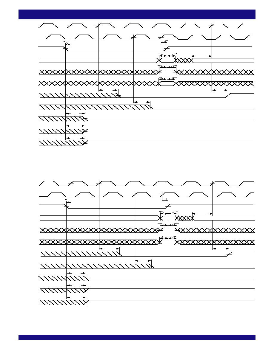
18
COMMERCIAL TEMPERATURE RANGE
IDT72V3626/72V3636/72V3646 CMOS 3.3V TRIPLE BUS SyncFIFO
TM
WITH BUS-MATCHING 256 x 36 x 2, 512 x 36 x 2, 1,024 x 36 x 2
NOTES:
1.
PRS2 and MBC must be HIGH during Master Reset until the rising edge of FFC/IRC goes HIGH.
2. If BE/
FWFT is HIGH, then EFA/ORA will go LOW one CLKA cycle earlier than in this case where BE/FWFT is LOW.
3.
MRS2 must toggle simultaneously with MRS1.
Figure 5. FIFO2 Master Reset and Loading X2 and Y2 with a Preset Value of Eight (IDT Standard and FWFT Modes)
Figure 4. FIFO1 Master Reset and Loading X1 and Y1 with a Preset Value of Eight (IDT Standard and FWFT Modes)
NOTES:
1.
PRS1 and MBC must be HIGH during Master Reset until the rising edge of FFA/IRA goes HIGH.
2. If BE/
FWFT is HIGH, then EFB/ORB will go LOW one CLKB cycle earlier than in this case where BE/FWFT is LOW.
CLKA
MRS1
FFA
/IRA
AEB
AFA
MBF1
CLKB
EFB
/ORB
FS1,FS0
4665 drw 05
t
RSTS
t
RSTH
t
FSH
t
FSS
t
WFF
t
WFF
t
REF
t
RSF
0,1
t
RSF
t
RSF
BE
BE/
FWFT
SPM
FWFT
t
BES
t
SPMS
t
BEH
t
SPMH
1
2
t
FWS
(2)
CLKC
MRS2
(3)
FFC
/IRC
AEA
AFC
MBF2
CLKA
EFA
/ORA
FS1,FS0
4665 drw 06
t
RSTS
t
RSTH
t
FSH
t
FSS
t
WFF
t
WFF
t
REF
t
RSF
0,1
t
RSF
t
RSF
BE
BE/
FWFT
SPM
FWFT
t
BES
t
SPMS
t
BEH
t
SPMH
1
2
t
FWS
(2)
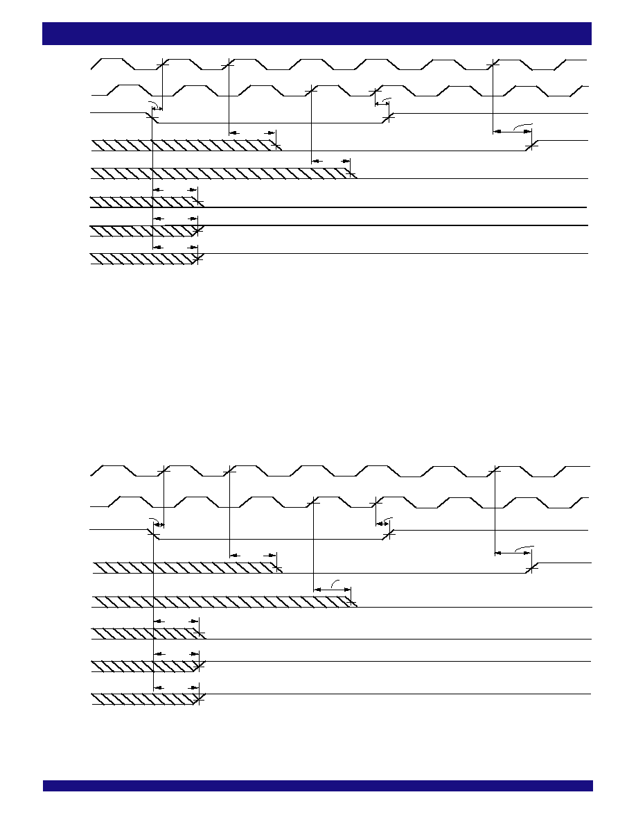
19
IDT72V3626/72V3636/72V3646 CMOS 3.3V Triple Bus SyncFIFO
TM
with Bus-Matching 256x36x2, 512x36x2, 1,024x36x2
COMMERCIAL TEMPERATURE RANGE
IDT72V3626/72V3636/72V3646 CMOS 3.3V TRIPLE BUS SyncFIFO
TM
WITH BUS-MATCHING 256 x 36 x 2, 512 x 36 x 2, 1,024 x 36 x 2
NOTES:
1.
MRS1 must be HIGH during Partial Reset.
2. If BE/
FWFT is HIGH, then EFB/ORB will go LOW one CLKB cycle earlier than in this case where BE/FWFT is LOW.
Figure 6. FIFO1 Partial Reset (IDT Standard and FWFT Modes)
Figure 7. FIFO2 Partial Reset (IDT Standard and FWFT Modes)
NOTES:
1.
MRS2 must be HIGH during Partial Reset.
2. If BE/
FWFT is HIGH, then EFA/ORA will go LOW one CLKA cycle earlier than in this case where BE/FWFT is LOW.
CLKA
PRS1
FFA
/IRA
AEB
AFA
MBF1
CLKB
EFB
/ORB
4665 drw 07
t
RSTS
t
RSTH
t
WFF
t
WFF
t
REF
t
RSF
t
RSF
t
RSF
1
2
(2)
CLKC
PRS2
FFC
/IRC
AEA
AFC
MBF1
CLKA
EFA
/ORA
4665 drw 08
t
RSTS
t
RSTH
t
WFF
t
WFF
t
REF
t
RSF
t
RSF
t
RSF
(2)
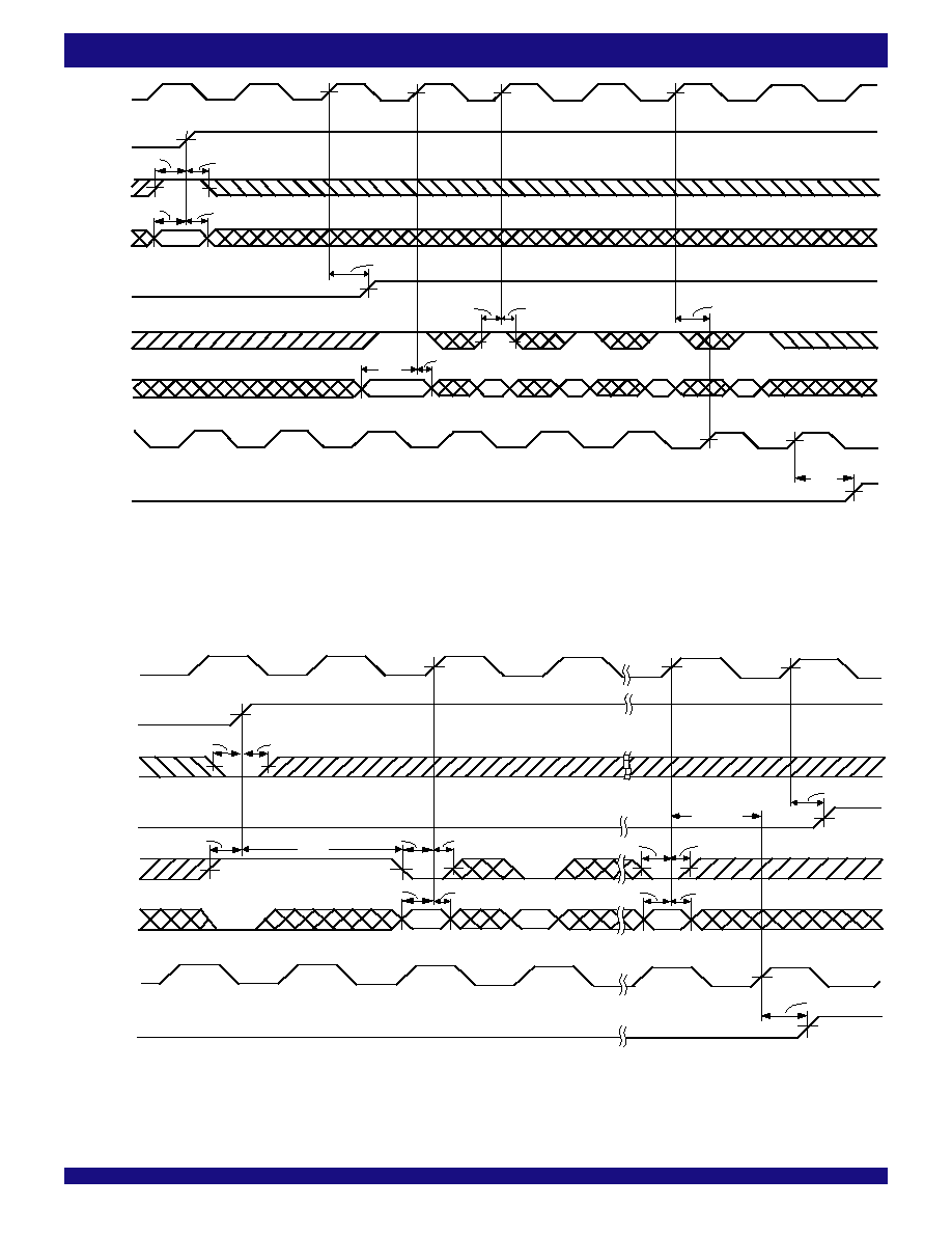
20
COMMERCIAL TEMPERATURE RANGE
IDT72V3626/72V3636/72V3646 CMOS 3.3V TRIPLE BUS SyncFIFO
TM
WITH BUS-MATCHING 256 x 36 x 2, 512 x 36 x 2, 1,024 x 36 x 2
Figure 9. Serial Programming of the Almost-Full Flag and Almost-Empty Flag Offset Values after Reset (IDT Standard and FWFT Modes)
NOTES:
1. t
SKEW1
is the minimum time between the rising CLKA edge and a rising CLKC edge for
FFC/IRC to transition HIGH in the next cycle. If the time between the rising edge of CLKA
and rising edge of CLKC is less than t
SKEW1
, then
FFC/IRC may transition HIGH one CLKC cycle later than shown.
2. It is not necessary to program Offset register bits on consecutive clock cycles. FIFO write attempts are ignored until
FFA/IRA, FFC/IRC is set HIGH.
3. Programmable offsets are written serially to the SD input in the order
AFA offset (Y1), AEB offset (X1), AFC offset (Y2), and AEA offset (X2).
NOTES:
1. t
SKEW1
is the minimum time between the rising CLKA edge and a rising CLKC edge for
FFC/IRC to transition HIGH in the next cycle. If the time between the rising edge of CLKA
and rising edge of CLKC is less than t
SKEW1
, then
FFC/IRC may transition HIGH one CLKC cycle later than shown.
2.
CSA = LOW, W/RA = HIGH, MBA = LOW. It is not necessary to program Offset register on consecutive clock cycles.
Figure 8. Parallel Programming of the Almost-Full Flag and Almost-Empty Flag Offset Values after Reset (IDT Standard and FWFT Modes)
4665 drw 09
CLKA
MRS1
,
MRS2
FFA
/IRA
CLKC
FFC
/IRC
A0-A35
FS1,FS0
ENA
t
FSH
t
WFF
t
ENH
t
ENS2
t
SKEW1
t
DS
t
DH
t
WFF
4
0,0
AFA
Offset
(Y1)
AEB
Offset
(X1)
AFC
Offset
(Y2)
AEA
Offset
(X2)
First Word to FIFO1
1
2
(1)
t
FSH
t
FSS
SPM
t
FSS
CLKA
FFA
/IRA
t
SENS
t
SENH
FS0/SD
(3)
t
SPH
t
SENS
t
SENH
t
FSS
t
WFF
FS1/
SEN
AEA
Offset
(X2) LSB
t
SDS
t
SDH
t
SDS
t
SDH
AFA
Offset
(Y1) MSB
MRS1
,
MRS2
4
4665 drw 10
t
FSS
t
FSH
CLKC
4
SPM
FFC
/IRC
t
WFF
t
SKEW(1)
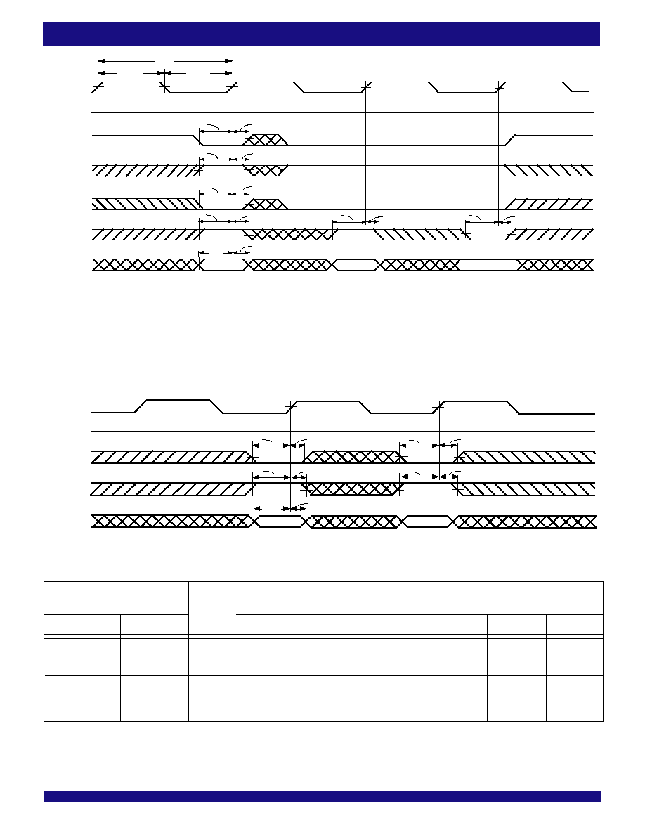
21
IDT72V3626/72V3636/72V3646 CMOS 3.3V Triple Bus SyncFIFO
TM
with Bus-Matching 256x36x2, 512x36x2, 1,024x36x2
COMMERCIAL TEMPERATURE RANGE
IDT72V3626/72V3636/72V3646 CMOS 3.3V TRIPLE BUS SyncFIFO
TM
WITH BUS-MATCHING 256 x 36 x 2, 512 x 36 x 2, 1,024 x 36 x 2
NOTE:
1. Written to FIFO1.
Figure 10. Port A Write Cycle Timing for FIFO1 (IDT Standard and FWFT Modes)
Figure 11. Port C Word Write Cycle Timing for FIFO2 (IDT Standard and FWFT Modes)
DATA SIZE TABLE .OR WORD WRITES TO .I.O2
NOTE:
1. BE is selected at Master Reset; SIZEB and SIZEC must be static throughout device operation.
SIZE MODE
(1)
WRITE
DATA WRITTEN
DATA READ FROM FIFO2
NO.
TO FIFO2
SIZEC
BE
C17-C9
C8-C0
A35-A27
A26-A18
A17-A9
A8-A0
L
H
1
A
B
A
B
C
D
2
C
D
L
L
1
C
D
A
B
C
D
2
A
B
4665 drw11
CLKA
FFA
/IRA
ENA
A0-A35
MBA
CSA
W/
R
A
t
CLK
t
CLKH
t
CLKL
t
ENH
t
ENH
t
ENH
t
ENH
t
DH
W1
(1)
W2
(1)
t
DS
t
ENS2
t
ENS1
t
ENH
t
ENH
No Operation
HIGH
t
ENS2
t
ENS2
t
ENS2
t
ENS2
CLKC
WENC
t
ENH
t
ENH
FFC
/IRC
HIGH
4665 drw12
C0-C17
t
ENH
t
ENH
MBC
t
DH
t
ENS2
t
DS
t
ENS2
t
ENS2
t
ENS2
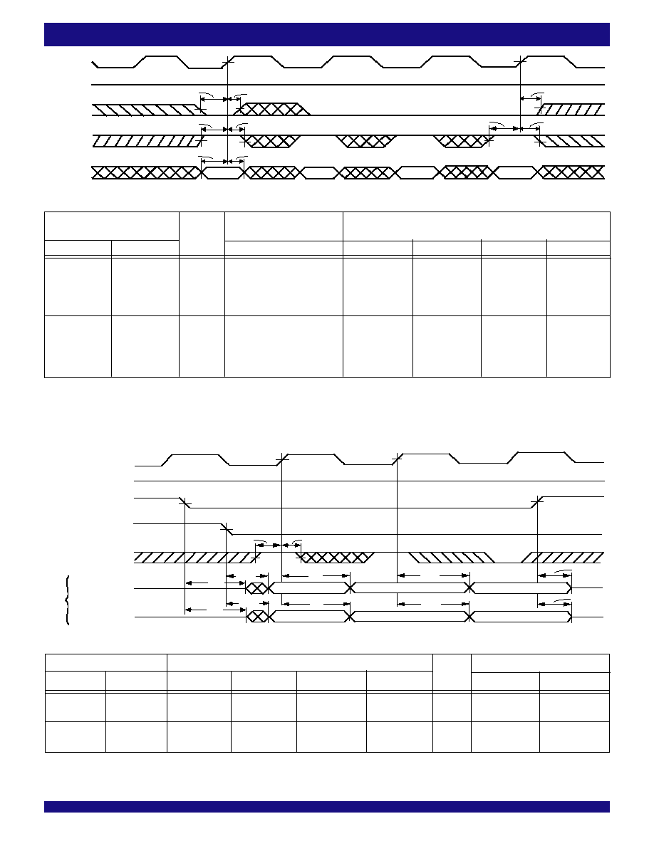
22
COMMERCIAL TEMPERATURE RANGE
IDT72V3626/72V3636/72V3646 CMOS 3.3V TRIPLE BUS SyncFIFO
TM
WITH BUS-MATCHING 256 x 36 x 2, 512 x 36 x 2, 1,024 x 36 x 2
DATA SIZE TABLE .OR WORD READS .ROM .I.O1
SIZE MODE
(1)
DATA WRITTEN TO FIFO1
READ
DATA READ FROM FIFO1
NO.
SIZEB
BE
A35-A27
A26-A18
A17-A9
A8-A0
B17-B9
B8-B0
H
H
A
B
C
D
1
A
B
2
C
D
H
L
A
B
C
D
1
C
D
2
A
B
Figure 13. Port B Word Read Cycle Timing for FIFO1 (IDT Standard and FWFT Modes)
Figure 12. Port C Byte Write Cycle Timing for FIFO2 (IDT Standard and FWFT Modes)
NOTE:
1. BE is selected at Master Reset; SIZEB and SIZEC must be static throughout device operation.
SIZE MODE
(1)
WRITE
DATA WRITTEN
DATA READ FROM FIFO2
NO.
TO FIFO2
SIZEC
BE
C8-C0
A35-A27
A26-A18
A17-A9
A8-A0
H
H
A
B
C
D
H
L
A
B
C
D
1
A
2
B
3
C
4
D
1
D
2
C
3
B
4
A
DATA SIZE TABLE .OR BYTE WRITES TO .I.O2
NOTE:
1. BE is selected at Master Reset; SIZEB and SIZEC must be static throughout device operation.
FFC
/IRC
CLKC
t
ENH
t
ENS2
WENC
4665 drw 13
HIGH
C0-C8
t
ENS2
t
ENH
t
ENS2
t
ENH
t
DS
t
DH
t
ENH
MBC
CLKB
RENB
EFB
/ORB
CSB
HIGH
4665 drw 14
B0-B17
Previous Data
t
DIS
t
A
t
A
t
ENS2
t
ENH
No Operation
Read 1
B0-B17
t
A
t
A
Read 1
Read 2
Read 2
Read 3
t
DIS
MBB
(Standard Mode)
(FWFT Mode)
OR
t
EN
t
MDV
t
MDV
t
EN
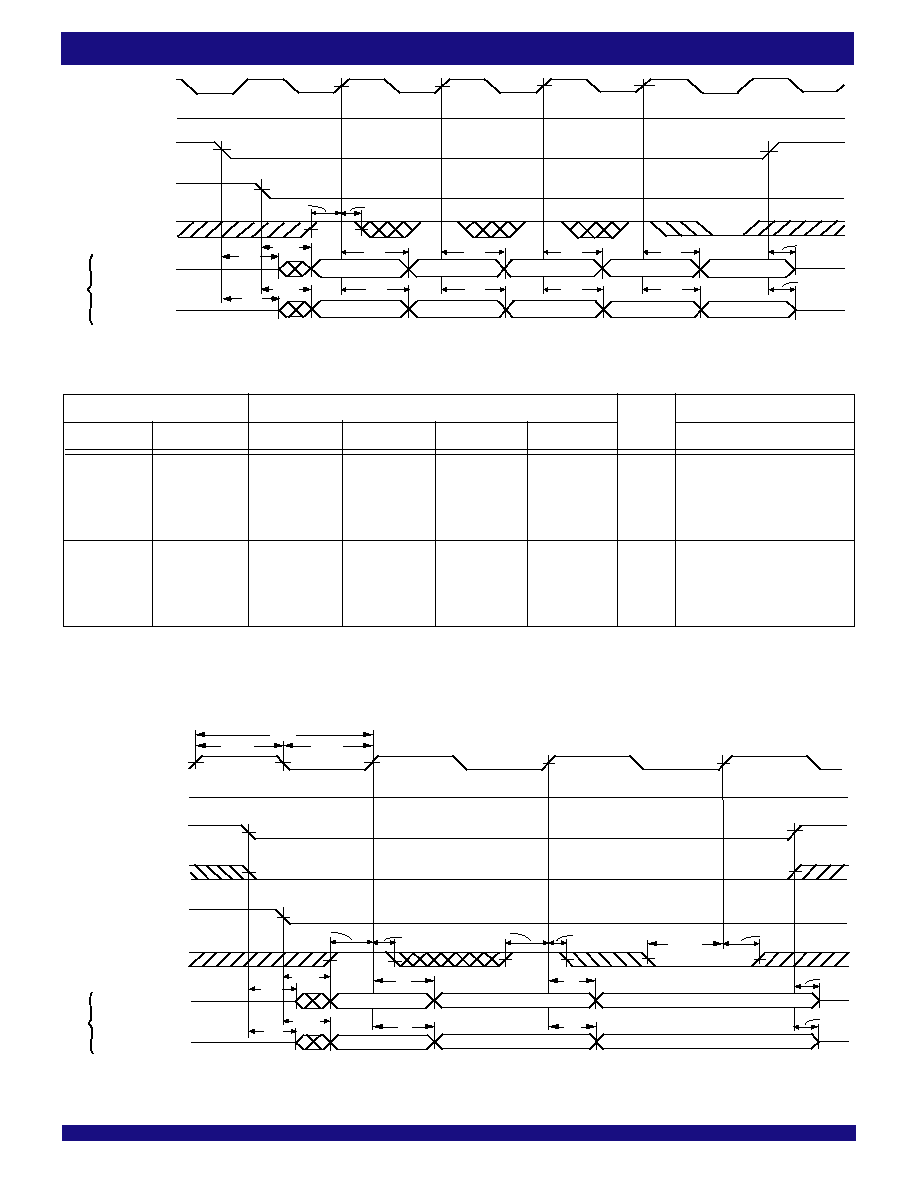
23
IDT72V3626/72V3636/72V3646 CMOS 3.3V Triple Bus SyncFIFO
TM
with Bus-Matching 256x36x2, 512x36x2, 1,024x36x2
COMMERCIAL TEMPERATURE RANGE
IDT72V3626/72V3636/72V3646 CMOS 3.3V TRIPLE BUS SyncFIFO
TM
WITH BUS-MATCHING 256 x 36 x 2, 512 x 36 x 2, 1,024 x 36 x 2
DATA SIZE TABLE .OR BYTE READS .ROM .I.O1
SIZE MODE
(1)
DATA WRITTEN TO FIFO1
READ
DATA READ FROM FIFO1
NO.
SIZEB
BE
A35-A27
A26-A18
A17-A9
A8-A0
B8-B0
H
H
A
B
C
D
H
L
A
B
C
D
1
A
2
B
3
C
4
D
1
D
2
C
3
B
4
A
NOTE:
1. Unused bytes B9-B17 are indeterminate for byte-size reads.
NOTE:
1. BE is selected at Master Reset; SIZEB must be static throughout device operation.
Figure 14. Port B Byte Read Cycle Timing for FIFO1 (IDT Standard and FWFT Modes)
NOTE:
1. Read From FIFO2.
Figure 15. Port A Read Cycle Timing for FIFO2 (IDT Standard and FWFT Modes)
EFB
/ORB
MBB
CSB
RENB
CLKB
4665 drw 15
HIGH
B0-B8
B0-B8
Read 5
Read 2
Read 3
Read 4
Read 1
Read 3
Read 4
Previous Data
Read 2
No Operation
t
DIS
t
DIS
t
A
t
A
t
A
t
A
t
A
t
A
t
ENS2
t
ENH
t
A
t
A
Read 1
(Standard Mode)
(FWFT Mode)
t
EN
t
MDV
t
MDV
t
EN
OR
4665 drw16
CLKA
EFA
/ORA
ENA
MBA
CSA
W/
R
A
t
CLK
t
CLKH
t
CLKL
t
ENS2
t
A
t
MDV
t
EN
t
A
t
ENH
t
ENH
W1
(1)
t
ENH
t
DIS
No Operation
A0-A35
t
EN
t
DIS
Previous Data
t
MDV
t
A
OR
t
A
W2
(1)
W1
(1)
W2
(1)
W3
(1)
(FWFT Mode)
(
Standard Mode)
A0-A35
HIGH
t
ENS2
t
ENS2
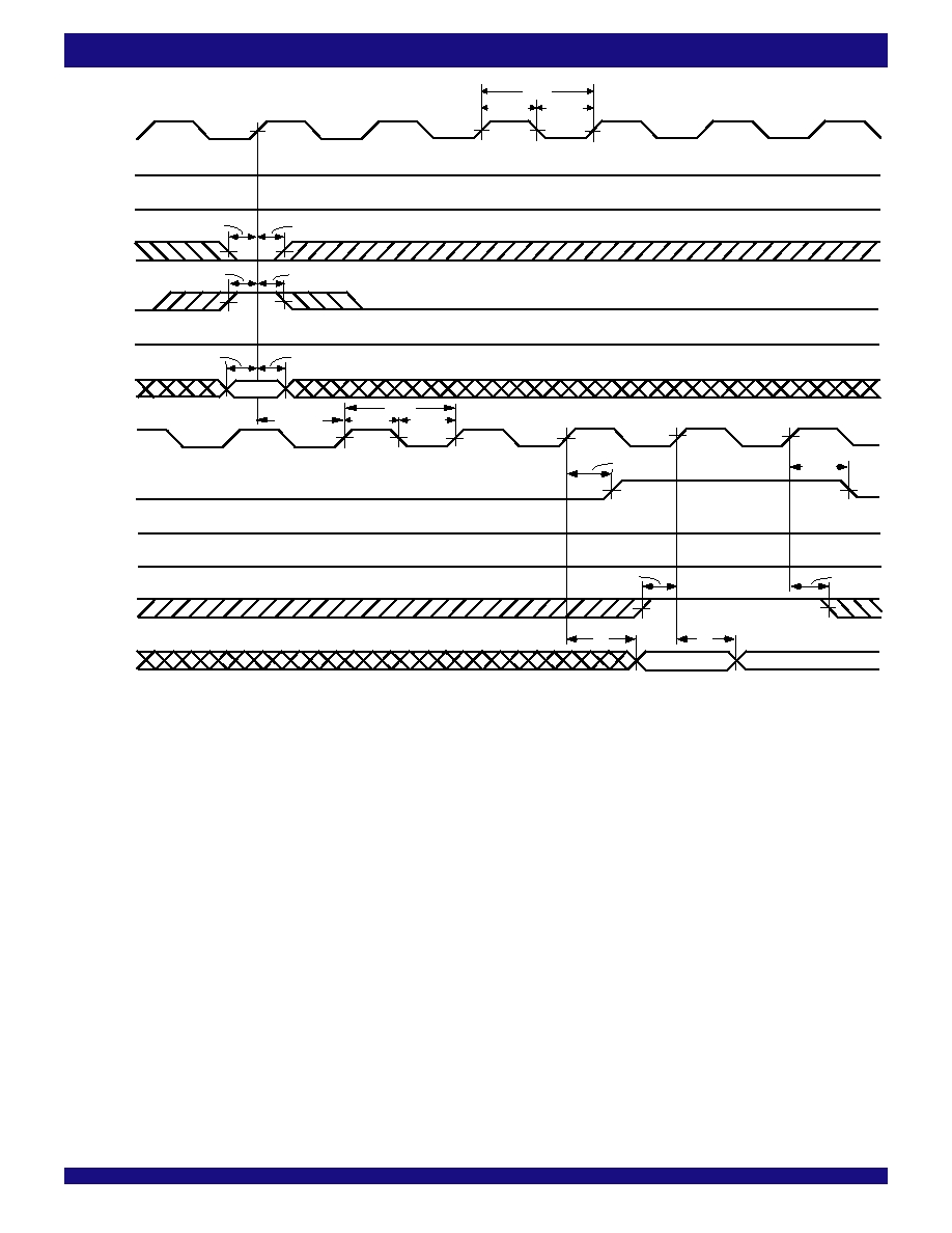
24
COMMERCIAL TEMPERATURE RANGE
IDT72V3626/72V3636/72V3646 CMOS 3.3V TRIPLE BUS SyncFIFO
TM
WITH BUS-MATCHING 256 x 36 x 2, 512 x 36 x 2, 1,024 x 36 x 2
NOTES:
1. t
SKEW1
is the minimum time between a rising CLKA edge and a rising CLKB edge for ORB to transition HIGH and to clock the next word to the FIFO1 output register in three CLKB cycles.
If the time between the rising CLKA edge and rising CLKB edge is less than t
SKEW1
, then the transition of ORB HIGH and load of the first word to the output register may occur one CLKB
cycle later than shown.
2. If Port B size is word or byte, ORB is set LOW by the last word or byte read from FIFO1, respectively (the word-size case is shown).
Figure 16. ORB Flag Timing and First Data Word Fall Through when FIFO1 is Empty (FWFT Mode)
CSA
W
R
A
MBA
A0-A35
CLKB
ORB
CSB
MBB
ENA
RENB
B0-B17
CLKA
1
2
4665 drw17
t
CLKH
t
CLKL
t
CLK
t
ENS2
t
ENS2
t
ENH
t
ENH
t
DS
t
DH
t
SKEW1
t
CLK
t
CLKL
t
ENS2
t
A
Read 1
FIFO1 Empty
LOW
HIGH
LOW
LOW
t
CLKH
W1
HIGH
(1)
t
REF
t
REF
Read 2
t
ENH
t
A
IRA
3
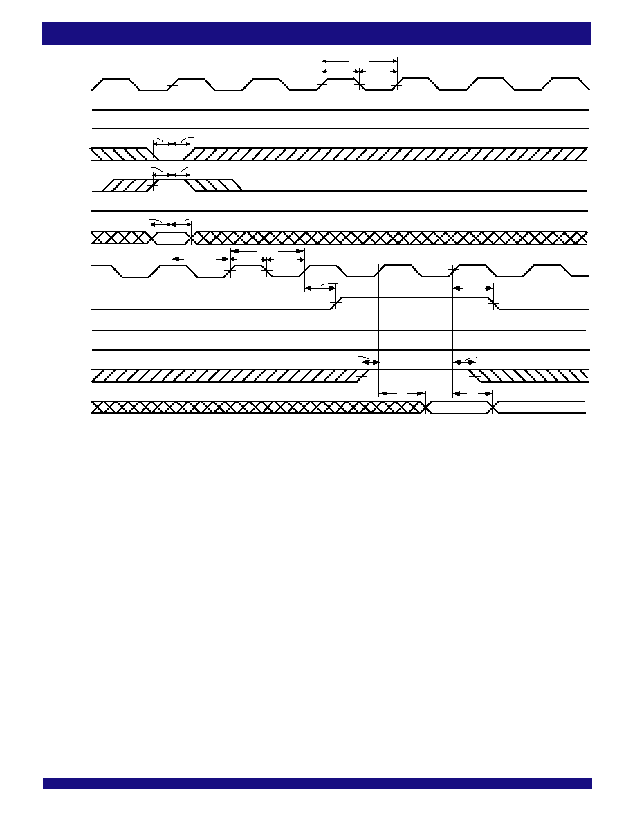
25
IDT72V3626/72V3636/72V3646 CMOS 3.3V Triple Bus SyncFIFO
TM
with Bus-Matching 256x36x2, 512x36x2, 1,024x36x2
COMMERCIAL TEMPERATURE RANGE
IDT72V3626/72V3636/72V3646 CMOS 3.3V TRIPLE BUS SyncFIFO
TM
WITH BUS-MATCHING 256 x 36 x 2, 512 x 36 x 2, 1,024 x 36 x 2
NOTES:
1. t
SKEW1
is the minimum time between a rising CLKA edge and a rising CLKB edge for
EFB to transition HIGH in the next CLKB cycle. If the time between the rising CLKA edge
and rising CLKB edge is less than t
SKEW1
, then the transition of
EFB HIGH may occur one CLKB cycle later than shown.
2. If Port B size is word or byte,
EFB is set LOW by the last word or byte read from FIFO1, respectively (the word-size case is shown).
Figure 17.
EFB
Flag Timing and First Data Read Fall Through when FIFO1 is Empty (IDT Standard Mode)
CSA
W
R
A
MBA
FFA
A0-A35
CLKB
CSB
MBB
ENA
RENB
B0-B17
CLKA
1
2
4665 drw18
t
CLKH
t
CLKL
t
CLK
t
ENS2
t
ENS2
t
ENH
t
ENH
t
DS
t
DH
t
SKEW1
t
CLK
t
CLKL
t
ENS2
t
A
Read 1
FIFO1 Empty
LOW
HIGH
LOW
LOW
t
CLKH
W1
HIGH
(1)
t
REF
t
REF
Read 2
t
ENH
t
A
EFB
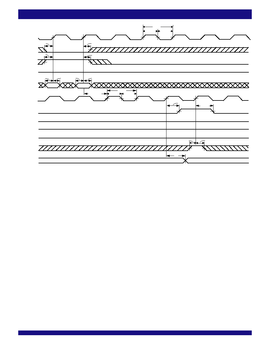
26
COMMERCIAL TEMPERATURE RANGE
IDT72V3626/72V3636/72V3646 CMOS 3.3V TRIPLE BUS SyncFIFO
TM
WITH BUS-MATCHING 256 x 36 x 2, 512 x 36 x 2, 1,024 x 36 x 2
NOTES:
1. t
SKEW1
is the minimum time between a rising CLKC edge and a rising CLKA edge for ORA to transition HIGH and to clock the next word to the FIFO2 output register in three CLKA cycles.
If the time between the CLKC edge and the rising CLKA edge is less than t
SKEW1
, then the transition of ORA HIGH and load of the first word to the output register may occur one CLKA
cycle later than shown.
2. If Port C size is word or byte, t
SKEW1
is referenced to the rising CLKC edge that writes the last word or byte write of the long word, respectively.
Figure 18. ORA Flag Timing and First Data Word Fall through when FIFO2 is Empty (FWFT Mode)
MBC
C0-C17
CLKA
CSA
W/
R
A
MBA
WENC
ENA
A0-A35
CLKC
1
2
4665 drw19
t
CLKH
t
CLKL
t
CLK
t
ENS2
t
ENS2
t
ENH
t
ENH
t
DS
t
DH
t
SKEW1
t
CLK
t
CLKL
t
ENS2
t
ENH
t
A
W1
FIFO2 Empty
LOW
LOW
LOW
t
CLKH
HIGH
(1)
t
REF
t
DH
t
DS
Write 1
Write 2
ORA
IRC
3
Old Data in FIFO2 Output Register
t
REF
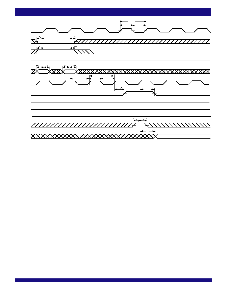
27
IDT72V3626/72V3636/72V3646 CMOS 3.3V Triple Bus SyncFIFO
TM
with Bus-Matching 256x36x2, 512x36x2, 1,024x36x2
COMMERCIAL TEMPERATURE RANGE
IDT72V3626/72V3636/72V3646 CMOS 3.3V TRIPLE BUS SyncFIFO
TM
WITH BUS-MATCHING 256 x 36 x 2, 512 x 36 x 2, 1,024 x 36 x 2
NOTES:
1. t
SKEW1
is the minimum time between a rising CLKC edge and a rising CLKA edge for
EFA to transition HIGH in the next CLKA cycle. If the time between the rising CLKC edge
and rising CLKA edge is less than t
SKEW1
, then the transition of
EFA HIGH may occur one CLKA cycle later than shown.
2. If Port C size is word or byte, t
SKEW1
is referenced to the rising CLKC edge that writes the last word or byte of the long word, respectively.
Figure 19.
EFA
Flag Timing and First Data Read when FIFO2 is Empty (IDT Standard Mode)
MBC
FFC
C0-C17
CLKA
EFA
CSA
W/
R
A
MBA
WENC
ENA
A0-A35
CLKC
1
2
4665 drw20
t
CLKH
t
CLKL
t
CLK
t
ENS2
t
ENS2
t
ENH
t
ENH
t
DS
t
DH
t
SKEW1
t
CLK
t
CLKL
t
ENS2
t
ENH
t
A
W1
FIFO2 Empty
LOW
LOW
LOW
t
CLKH
HIGH
(1)
t
REF
t
REF
t
DH
t
DS
Write 1
Write 2
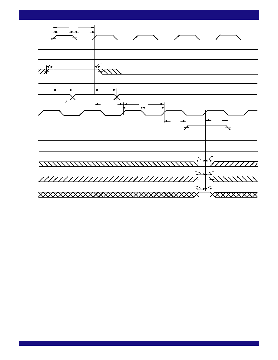
28
COMMERCIAL TEMPERATURE RANGE
IDT72V3626/72V3636/72V3646 CMOS 3.3V TRIPLE BUS SyncFIFO
TM
WITH BUS-MATCHING 256 x 36 x 2, 512 x 36 x 2, 1,024 x 36 x 2
NOTES:
1. t
SKEW1
is the minimum time between a rising CLKB edge and a rising CLKA edge for IRA to transition HIGH in the next CLKA cycle. If the time between the rising CLKB edge and rising
CLKA edge is less than t
SKEW1
, then IRA may transition HIGH one CLKA cycle later than shown.
2. If Port B size is word or byte, t
SKEW1
is referenced to the rising CLKB edge that reads the last word or byte write of the long word, respectively (the word-size case is shown).
Figure 20. IRA Flag Timing and First Available Write when FIFO1 is Full (FWFT Mode)
CSB
MBB
RENB
B0-B17
CLKB
CLKA
CSA
4665 drw21
W/
R
A
1
2
A0-A35
MBA
ENA
t
CLK
t
CLKH
t
CLKL
t
ENS2
t
ENH
t
A
t
SKEW1
t
CLK
t
CLKH
t
CLKL
t
ENS2
t
ENS2
t
DS
t
ENH
t
ENH
t
DH
To FIFO1
Read 2
LOW
LOW
HIGH
LOW
HIGH
(1)
FIFO1 Full
t
WFF
t
WFF
Read 1
t
A
Previous Word in
FIFO1 Output Register
ORB
IRA
Write
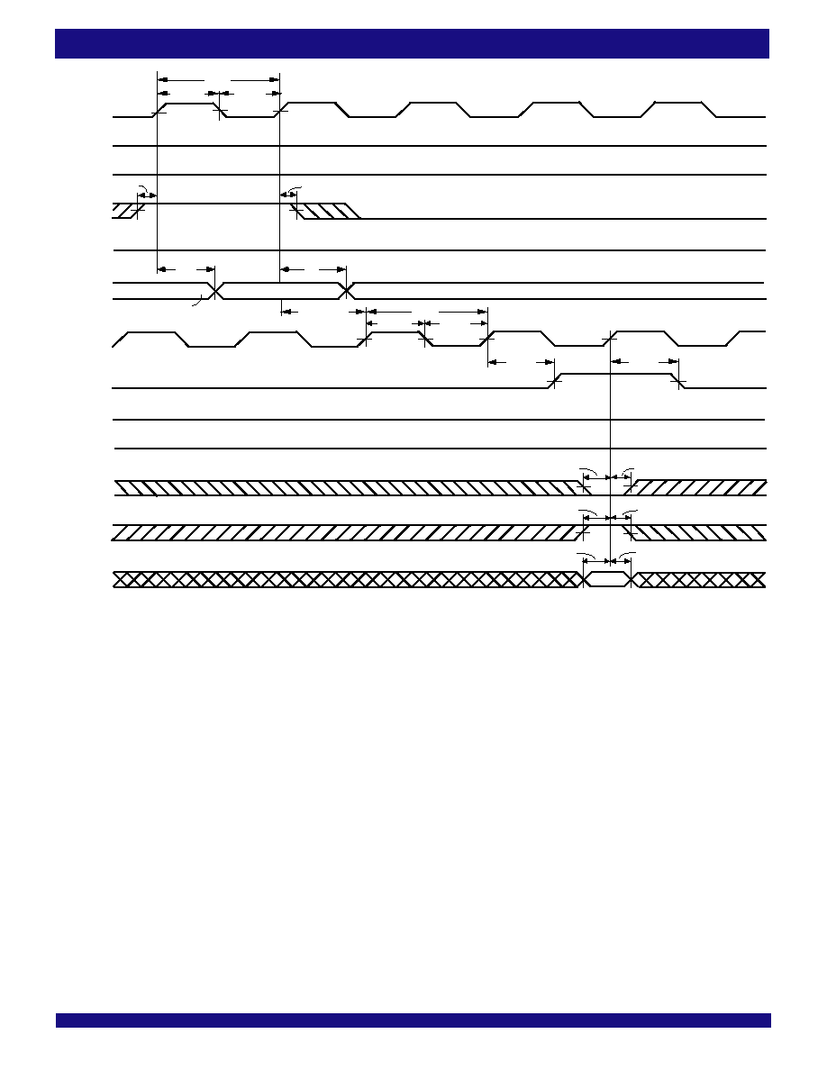
29
IDT72V3626/72V3636/72V3646 CMOS 3.3V Triple Bus SyncFIFO
TM
with Bus-Matching 256x36x2, 512x36x2, 1,024x36x2
COMMERCIAL TEMPERATURE RANGE
IDT72V3626/72V3636/72V3646 CMOS 3.3V TRIPLE BUS SyncFIFO
TM
WITH BUS-MATCHING 256 x 36 x 2, 512 x 36 x 2, 1,024 x 36 x 2
NOTES:
1. t
SKEW1
is the minimum time between a rising CLKB edge and a rising CLKA edge for
FFA to transition HIGH in the next CLKA cycle. If the time between the rising CLKB edge
and rising CLKA edge is less than t
SKEW1
, then
FFA may transition HIGH one CLKA cycle later than shown.
2. If Port B size is word or byte, t
SKEW1
is referenced from the rising CLKB edge that reads the last word or byte of the long word, respectively (the word-size case is shown).
Figure 21.
FFA
Flag Timing and First Available Write when FIFO1 is Full (IDT Standard Mode)
CSB
EFB
MBB
RENB
B0-B17
CLKB
FFA
CLKA
CSA
4665 drw22
W/
R
A
1
2
A0-A35
MBA
ENA
t
CLK
t
CLKH
t
CLKL
t
ENS2
t
ENH
t
A
t
SKEW1
t
CLK
t
CLKH
t
CLKL
t
ENS2
t
ENS2
t
DS
t
ENH
t
ENH
t
DH
To FIFO1
Read 2
LOW
LOW
HIGH
LOW
HIGH
(1)
FIFO1 Full
t
WFF
t
WFF
Read 1
t
A
Previous Word in
FIFO1 Output Register
Write
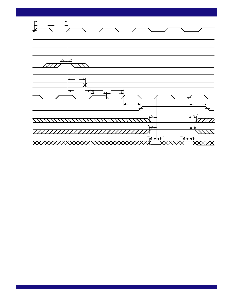
30
COMMERCIAL TEMPERATURE RANGE
IDT72V3626/72V3636/72V3646 CMOS 3.3V TRIPLE BUS SyncFIFO
TM
WITH BUS-MATCHING 256 x 36 x 2, 512 x 36 x 2, 1,024 x 36 x 2
NOTES:
1. t
SKEW1
is the minimum time between a rising CLKC edge and a rising CLKC edge for IRC to transition HIGH in the next CLKC cycle. If the time between the rising CLKA edge and rising
CLKC edge is less than t
SKEW1
, then IRC may transition HIGH one CLKC cycle later than shown.
2. If Port C size is word or byte, IRC is set LOW by the last word or byte write of the long word, respectively (the word-size case is shown).
Figure 22. IRC Flag Timing and First Available Write when FIFO2 is Full (FWFT Mode)
CSA
ORA
MBA
ENA
A0-A35
CLKA
IRC
CLKC
4665 drw23
1
2
C0-C17
MBC
WENC
t
CLK
t
CLKH
t
CLKL
t
ENS2
t
ENH
t
A
t
SKEW1
t
CLK
t
CLKH
t
CLKL
t
ENS2
t
ENS2
t
DS
t
ENH
t
ENH
t
DH
To FIFO2
Previous Word in FIFO2 Output Register
Next Word From FIFO2
LOW
W/
R
A
LOW
LOW
HIGH
(1)
FIFO2 Full
t
WFF
t
DH
t
DS
t
WFF
Write
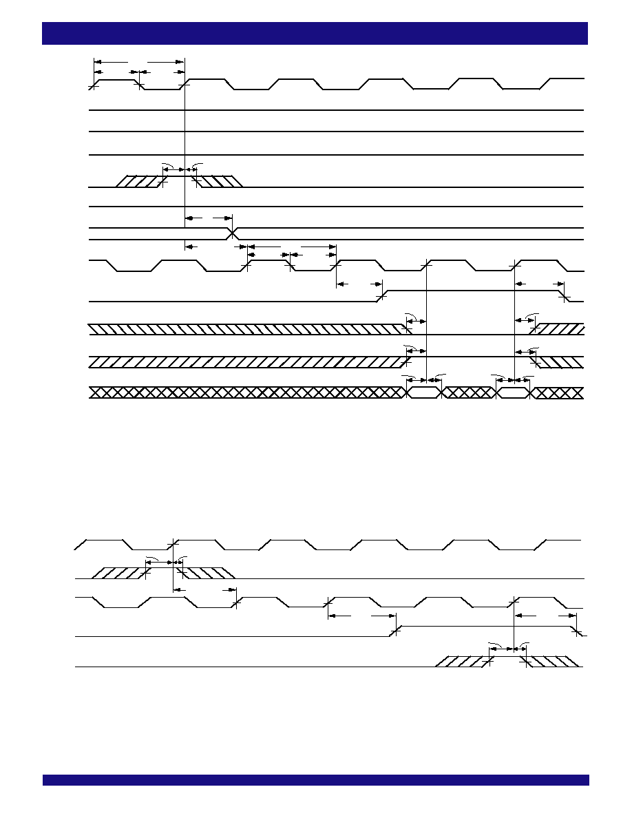
31
IDT72V3626/72V3636/72V3646 CMOS 3.3V Triple Bus SyncFIFO
TM
with Bus-Matching 256x36x2, 512x36x2, 1,024x36x2
COMMERCIAL TEMPERATURE RANGE
IDT72V3626/72V3636/72V3646 CMOS 3.3V TRIPLE BUS SyncFIFO
TM
WITH BUS-MATCHING 256 x 36 x 2, 512 x 36 x 2, 1,024 x 36 x 2
NOTES:
1. t
SKEW2
is the minimum time between a rising CLKA edge and a rising CLKB edge for
AEB to transition HIGH in the next CLKB cycle. If the time between the rising CLKA edge
and rising CLKB edge is less than t
SKEW2
, then
AEB may transition HIGH one CLKB cycle later than shown.
2. FIFO1 Write (
CSA = LOW, W/RA = LOW, MBA = LOW), FIFO1 read (CSB = LOW, MBB = LOW). Data in the FIFO1 output register has been read from the FIFO.
3. If Port B size is word or byte,
AEB is set LOW by the last word or byte read from FIFO1, respectively.
Figure 24. Timing for
AEB
when FIFO1 is Almost-Empty (IDT Standard and FWFT Modes)
Figure 23.
FFC
Flag Timing and First Available Write when FIFO2 is Full (IDT Standard Mode)
NOTES:
1. t
SKEW1
is the minimum time between a rising CLKA edge and a rising CLKC edge for
FFC to transition HIGH in the next CLKC cycle. If the time between the rising CLKA edge
and rising CLKC edge is less than t
SKEW1
, then
FFC may transition HIGH one CLKC cycle later than shown.
2. If Port C size is word or byte,
FFC is set LOW by the last word or byte write of the long word, respectively (the word-size case is shown).
CSA
EFA
MBA
ENA
A0-A35
CLKA
FFC
CLKC
4665 drw24
1
2
C0-C17
MBC
ENC
t
CLK
t
CLKH
t
CLKL
t
ENS2
t
ENH
t
A
t
SKEW1
t
CLK
t
CLKH
t
CLKL
t
ENS2
t
ENS2
t
DS
t
ENH
t
ENH
t
DH
To FIFO2
Previous Word in FIFO2 Output Register
Next Word From FIFO2
LOW
W/
R
A
LOW
LOW
HIGH
(1)
FIFO2 Full
t
WFF
t
WFF
t
DH
t
DS
Write
AEB
CLKA
RENB
4665 drw25
ENA
CLKB
2
1
t
ENS2
t
ENH
t
SKEW2
t
PAE
t
PAE
t
ENS2
t
ENH
X1 Word in FIFO1
(X1+1) Words in FIFO1
(1)
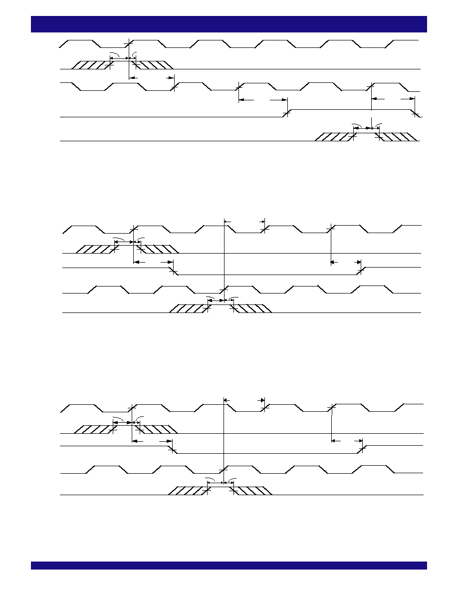
32
COMMERCIAL TEMPERATURE RANGE
IDT72V3626/72V3636/72V3646 CMOS 3.3V TRIPLE BUS SyncFIFO
TM
WITH BUS-MATCHING 256 x 36 x 2, 512 x 36 x 2, 1,024 x 36 x 2
NOTES:
1. t
SKEW2
is the minimum time between a rising CLKC edge and a rising CLKA edge for
AFC to transition HIGH in the next CLKC cycle. If the time between the rising CLKC edge
and rising CLKA edge is less than t
SKEW2
, then
AFC may transition HIGH one CLKC cycle later than shown.
2. FIFO2 write (MBC = LOW), FIFO2 read (
CSA = LOW, W/RA = LOW, MBA = LOW). Data in the FIFO2 output register has been read from the FIFO.
3. D = Maximum FIFO Depth = 256 for the IDT72V3626, 512 for the IDT72V3636, 1,024 for the IDT72V3646.
4. Port C size is word or byte,
AFC is set LOW by the last word or byte write of the long word, respectively.
Figure 27. Timing for
AFC
when FIFO2 is Almost-Full (IDT Standard and FWFT Modes)
Figure 25. Timing for
AEA
when FIFO2 is Almost-Empty (IDT Standard and FWFT Modes)
Figure 26. Timing for
AFA
when FIFO1 is Almost-Full (IDT Standard and FWFT Modes)
NOTES:
1. t
SKEW2
is the minimum time between a rising CLKC edge and a rising CLKA edge for
AEA to transition HIGH in the next CLKA cycle. If the time between the rising CLKC edge
and rising CLKA edge is less than t
SKEW2
, then
AEA may transition HIGH one CLKA cycle later than shown.
2. FIFO2 Write (MBC = LOW), FIFO2 read (
CSA = LOW, W/RA = LOW, MBA = LOW). Data in the FIFO2 output register has been read from the FIFO.
3. If Port C size is word or byte, t
SKEW2
is referenced to the rising CLKC edge that writes the last word or byte of the long word, respectively.
NOTES:
1. t
SKEW2
is the minimum time between a rising CLKA edge and a rising CLKB edge for
AFA to transition HIGH in the next CLKA cycle. If the time between the rising CLKA edge
and rising CLKB edge is less than t
SKEW2
, then
AFA may transition HIGH one CLKA cycle later than shown.
2. FIFO1 Write (
CSA = LOW, W/RA = HIGH, MBA = LOW), FIFO1 read (CSB = LOW, MBB = LOW). Data in the FIFO1 output register has been read from the FIFO.
3. D = Maximum FIFO Depth = 256 for the IDT72V3626, 512 for the IDT72V3636, 1,024 for the IDT72V3646.
4. If Port B size is word or byte, t
SKEW2
is referenced from the rising CLKB edge that reads the last word or byte of the long word, respectively.
AEA
CLKC
ENA
4665 drw 26
WENC
CLKA
2
1
t
ENS2
t
ENH
t
SKEW2
t
PAE
t
PAE
t
ENS2
t
ENH
(X2+1) Words in FIFO2
X2 Words in FIFO2
(1)
AFA
CLKA
RENB
4665 drw 27
ENA
CLKB
1
2
t
SKEW2
t
ENS2
t
ENH
t
PAF
t
ENS2
t
ENH
t
PAF
[D-(Y1+1)] Words in FIFO1
(D-Y1) Words in FIFO1
(1)
AFC
CLKC
ENA
4665 drw 28
WENC
CLKA
1
2
t
SKEW2
t
ENS2
t
ENH
t
PAF
t
ENS2
t
ENH
t
PAF
[D-(Y2+1)] Words in FIFO2
(D-Y2) Words in FIFO2
(1)
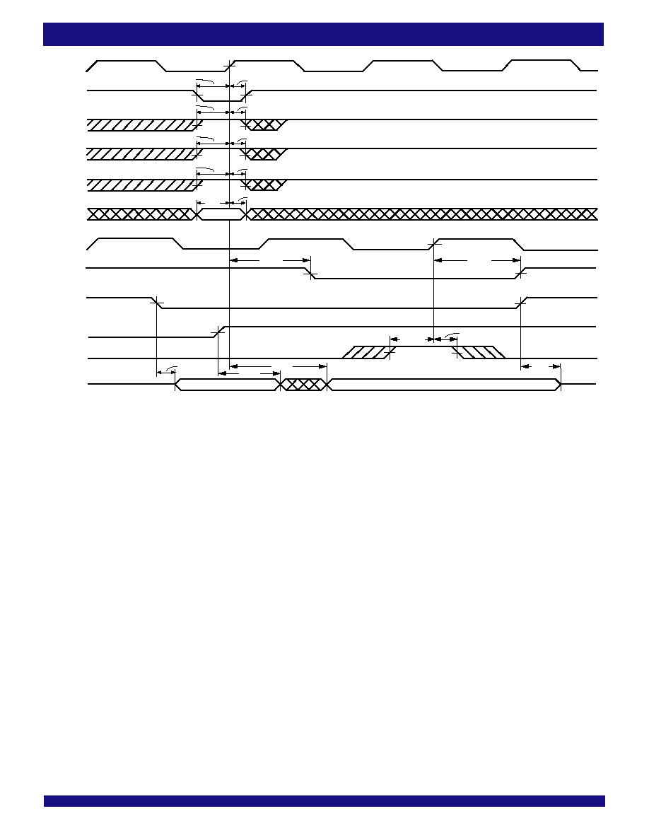
33
IDT72V3626/72V3636/72V3646 CMOS 3.3V Triple Bus SyncFIFO
TM
with Bus-Matching 256x36x2, 512x36x2, 1,024x36x2
COMMERCIAL TEMPERATURE RANGE
IDT72V3626/72V3636/72V3646 CMOS 3.3V TRIPLE BUS SyncFIFO
TM
WITH BUS-MATCHING 256 x 36 x 2, 512 x 36 x 2, 1,024 x 36 x 2
Figure 28. Timing for Mail1 Register and
MBF1
Flag (IDT Standard and FWFT Modes)
4665 drw29
CLKA
ENA
A0-A35
MBA
CSA
W/
R
A
CLKB
MBF1
CSB
MBB
RENB
B0-B17
W1
t
ENS1
t
ENH
t
DS
t
DH
t
PMF
t
PMF
t
ENS2
t
ENH
t
DIS
t
EN
t
MDV
t
PMR
FIFO1 Output Register
W1 (Remains valid in Mail1 Register after read)
t
ENS2
t
ENH
t
ENS2
t
ENH
t
ENH
t
ENS2
NOTE:
1. If Port B is configured for word size, data can be written to the Mail1 register using A0-A17 (A18-A35 are don't care inputs). In this first case B0-B17 will have valid data. If Port
B is configured for byte size, data can be written to the Mail1 Register using A0-A8 (A9-A35 are don't care inputs). In this second case, B0-B8 will have valid data (B9-B17 will
be indeterminate).
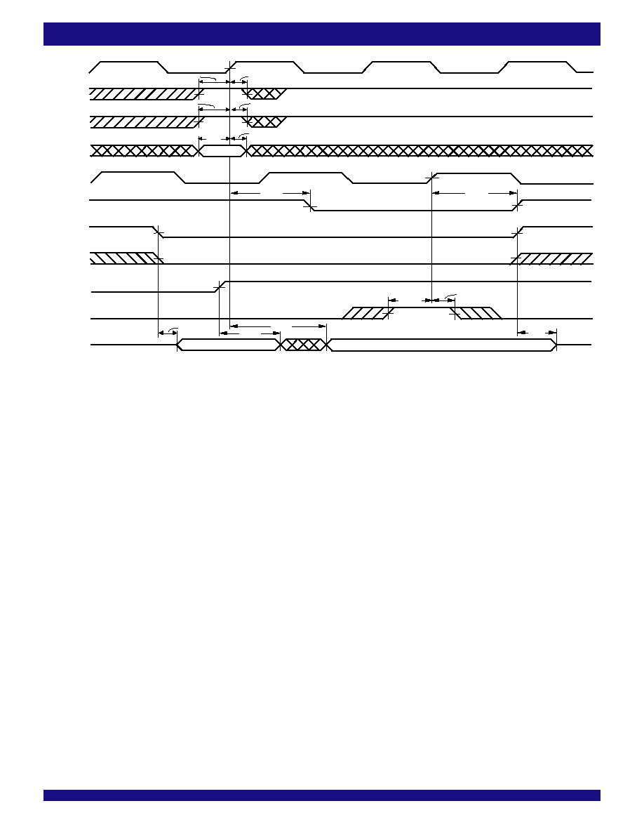
34
COMMERCIAL TEMPERATURE RANGE
IDT72V3626/72V3636/72V3646 CMOS 3.3V TRIPLE BUS SyncFIFO
TM
WITH BUS-MATCHING 256 x 36 x 2, 512 x 36 x 2, 1,024 x 36 x 2
Figure 29. Timing for Mail2 Register and
MBF2
Flag (IDT Standard and FWFT Modes)
4665 drw30
CLKC
ENC
C0-C17
MBC
CLKA
MBF2
CSA
MBA
ENA
A0-A35
W/
R
A
W1
t
DS
t
DH
t
PMF
t
PMF
t
ENH
t
DIS
t
EN
t
MDV
t
PMR
FIFO2 Output Register
W1 (Remains valid in Mail2 Register after read)
t
ENS2
t
ENH
t
ENS2
t
ENH
t
ENS2
NOTE:
1. If Port C is configured for word size, data can be written to the Mail2 register using C0-C17. In this first case, A18-A35 will have valid data (A0-A17 will be indeterminate). If Port C is configured
for byte size, data can be written to the Mail2 register using C0-C8 (C9-C17 are don't care inputs). In this second case, A18-A26 will have valid data (A0-A17 and A27-A35 will be
indeterminate).
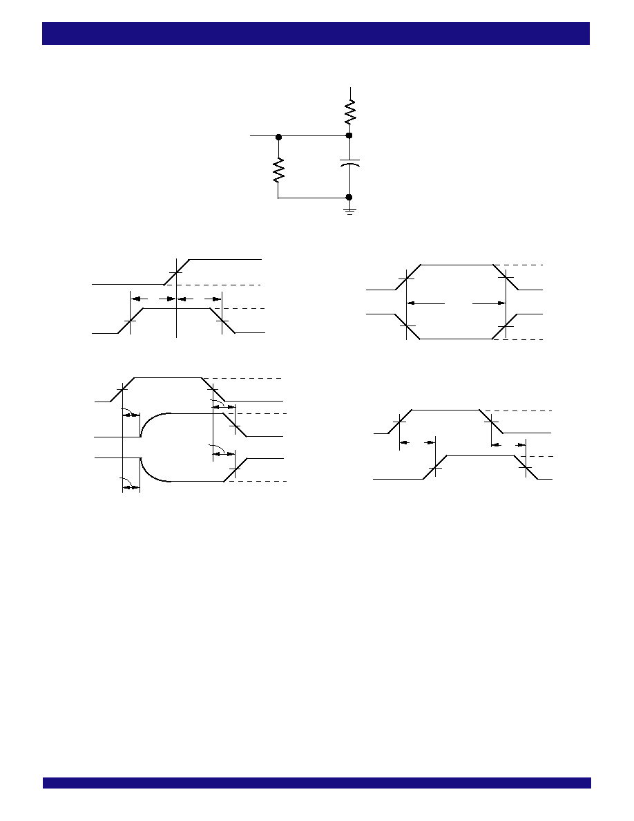
35
IDT72V3626/72V3636/72V3646 CMOS 3.3V Triple Bus SyncFIFO
TM
with Bus-Matching 256x36x2, 512x36x2, 1,024x36x2
COMMERCIAL TEMPERATURE RANGE
IDT72V3626/72V3636/72V3646 CMOS 3.3V TRIPLE BUS SyncFIFO
TM
WITH BUS-MATCHING 256 x 36 x 2, 512 x 36 x 2, 1,024 x 36 x 2
NOTE:
1. Includes probe and jig capacitance.
Figure 30. Load Circuit and Voltage Waveforms
4665 drw31
PARAMETER MEASUREMENT INFORMATION
From Output
Under Test
30 pF
330
3.3V
510
PROPAGATION DELAY
LOAD CIRCUIT
3V
GND
Timing
Input
Data,
Enable
Input
GND
3V
1.5V
1.5V
VOLTAGE WAVEFORMS
SETUP AND HOLD TIMES
VOLTAGE WAVEFORMS
PULSE DURATIONS
VOLTAGE WAVEFORMS
ENABLE AND DISABLE TIMES
VOLTAGE WAVEFORMS
PROPAGATION DELAY TIMES
3V
GND
GND
3V
1.5V
1.5V
1.5V
1.5V
t
W
Output
Enable
Low-Level
Output
High-Level
Output
3V
OL
GND
3V
1.5V
1.5V
1.5V
1.5V
OH
OV
GND
OH
OL
1.5V
1.5V
1.5V
1.5V
Input
In-Phase
Output
High-Level
Input
Low-Level
Input
V
V
V
V
1.5V
3V
t
S
t
h
t
PLZ
t
PHZ
t
PZL
t
PZH
t
PD
t
PD
(1)
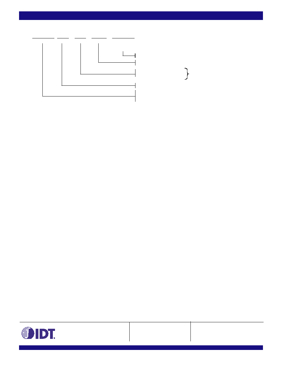
36
CORPORATE HEADQUARTERS
for SALES:
for TECH SUPPORT:
2975 Stender Way
800-345-7015 or 408-727-6116
408-330-1753
Santa Clara, CA 95054
fax: 408-492-8674
FIFOhelp@idt.com
www.idt.com
ORDERING IN.ORMATION
NOTE:
1. Industrial temperature range is available by special order.
BLANK
PF
L
72V3626
72V3636
72V3646
4665 drw 32
Commercial (0
∞
C to +70
∞
C)
Thin Quad Flat Pack (TQFP, PK128-1)
Low Power
256 x 36 x 2
3.3V Triple Bus SyncFIFO
with Bus-Matching
512 x 36 x 2
3.3V Triple Bus SyncFIFO
with Bus-Matching
1,024 x 36 x 2
3.3V Triple Bus SyncFIFO
with Bus-Matching
XXXXXX
IDT
Device Type
XX
X
Power
Speed
Package
Process/
Temperature
Range
X
XX
Clock Cycle Time (t
CLK
)
Speed in Nanoseconds
Commercial Only
10
15
DATASHEET DOCUMENT HISTORY
12/12/2000
pgs. 12 and 21.
03/21/2001
pgs. 6 and 7.
08/01/2001
pgs. 6, 8, 9 and 36.