 | –≠–ª–µ–∫—Ç—Ä–æ–Ω–Ω—ã–π –∫–æ–º–ø–æ–Ω–µ–Ω—Ç: 72V3651 | –°–∫–∞—á–∞—Ç—å:  PDF PDF  ZIP ZIP |
1
2000 Integrated Device Technology, Inc.
DSC-4658/-
©
AUGUST 2000
3.3 VOLT CMOS SyncFIFO
TM
512 x 36, 1,024 x 36,
and 2,048 x 36
PRELIMINARY
IDT72V3631
IDT72V3641
IDT72V3651
FEATURES:
Storage capacity:
IDT72V3631 - 512 x 36
IDT72V3641 - 1,024 x 36
IDT72V3651 - 2,048 x 36
Supports clock frequencies up to 67 MHz
Fast access times of 10ns
Free-running CLKA and CLKB can be asynchronous or coinci-
dent (permits simultaneous reading and writing of data on a
single clock edge)
Clocked FIFO buffering data from Port A to Port B
Synchronous read retransmit capability
Mailbox register in each direction
Programmable Almost-Full and Almost-Empty flags
Microprocessor interface control logic
Input Ready (IR) and Almost-Full (
AF) flags synchronized by
CLKA
Output Ready (OR) and Almost-Empty (
AE) flags synchronized
by CLKB
Available in 132-pin plastic quad flat package (PQFP) or space-
saving 120-pin thin quad flat package (TQFP)
Pin and functionally compatible versions of the 5V operating
IDT723631/723641/723651
Easily expandable in width and depth
Industrial temperature range (≠40
∞
∞
∞
∞
∞
C to +85
∞
∞
∞
∞
∞
C) is available
DESCRIPTION:
The IDT72V3631/72V3641/72V3651 are pin and functionally compat-
ible versons of the IDT723631/723641/723651, designed to run off a 3.3V
supply for exceptionally low-power consumption. These devices are
monolithic high-speed, low-power, CMOS clocked FIFO memory. It sup-
ports clock frequencies up to 67 MHz and has read access times as fast as
10ns. The 512/1,024/2,048 x 36 dual-port SRAM FIFO buffers data from
port A to Port B. The FIFO memory has retransmit capability, which allows
previously read data to be accessed again. The FIFO operates in First Word
Fall Through mode and has flags to indicate empty and full conditions and
conditions and two programmable flags (Almost-Full and Almost-Empty) to
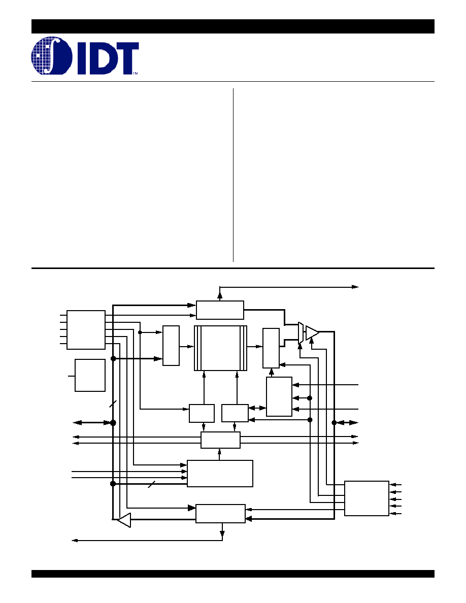
FUNCTIONAL BLOCK DIAGRAM
Mail 1
Register
Input
Register
Output
Register
CLKA
CSA
W/
R
A
ENA
MBA
Port-A
Control
Logic
Reset
Logic
RST
CLKB
CSB
W
/RB
ENB
MBB
Port-B
Control
Logic
MBF1
OR
AE
B
0
- B
35
4658 drw 01
Mail 2
Register
Write
Pointer
Read
Pointer
Status Flag
Logic
MBF2
IR
AF
FS
0
/SD
FS
1
/
SEN
Flag Offset
Registers
A
0
- A
35
10
Sync
Retransmit
Logic
RTM
RFM
RAM ARRAY
512 x 36
1,024 x 36
2,048 x 36
36
2
Commercial Temperature
IDT72V3631/72V3641/72V3651
3.3V CMOS SYNCFIFOTM 512 x 36, 1,024 x 36 AND 2,048 x 36
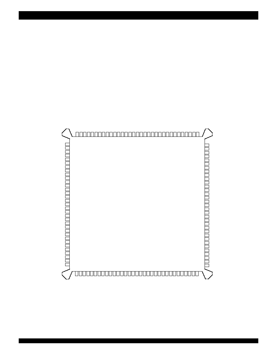
NC
NC
A
35
A
34
A
33
A
32
V
CC
A
31
A
30
GND
A
29
A
28
A
27
A
26
A
25
A
24
A
23
GND
A
22
V
CC
A
21
A
20
A
19
A
18
GND
A
17
A
16
A
15
A
14
A
13
V
CC
A
12
NC
NC
B
35
B
34
B
33
B
32
GND
B
31
B
30
B
29
B
28
B
27
B
26
V
CC
B
25
B
24
GND
B
23
B
22
B
21
B
20
B
19
B
18
GND
B
17
B
16
V
CC
B
15
B
14
B
13
B
12
GND
NC
NC
18
19
20
21
22
23
24
25
26
27
28
29
30
31
32
33
34
35
36
37
38
39
40
41
42
43
44
45
46
47
48
49
50
116
115
114
113
112
111
110
109
108
107
106
105
104
103
102
101
100
99
98
97
96
95
94
93
92
91
90
89
88
87
86
85
84
4658 drw 02
117
17
16
15
14
13
12
11
10
9
8
7
6
5
4
3
2
1
132
131
130
129
128
127
126
125
124
123
122
121
120
119
118
NC
NC
B
11
B
10
B
9
B
7
B
8
V
CC
B
6
GND
B
5
B
4
B
3
B
2
B
1
B
0
GND
A
0
A
1
A
2
V
CC
A
3
A
4
A
5
GND
A
6
A
7
A
8
A
9
A
10
A
11
GND
NC
51
52
53
54
55
56
57
58
59
60
61
62
63
64
65
66
67
68
69
70
71
72
73
74
75
76
77
78
79
80
81
82
83
NC
NC
NC V
CC
CLKB
ENB
W
/RB
CSB
GND
RFM
RTM
V
CC
MBF1
MBB
FS1/
SEN
GND
FS0/SD
RST
MBA
MBF2
AE AF
V
CC
IR
CSA
W/
R
A
ENA
CLKA
GND
GND
NC
V
CC
OR
DESCRIPTION (Continued)
NOTES:
1. NC ≠ No internal connection
2. Uses Yamaichi socket IC51-1324-828
PIN CONFIGURATION
*
Electrical pin 1 in center of beveled edge. Pin 1 identifier in corner.
*
PQFP (PQ132-1, order code: PQF)
TOP VIEW
indicate when a selected number of words is stored in memory. Communication
between each port may take place with two 36-bit mailbox registers. Each
mailbox register has a flag to signal when new mail has been stored. Two or
more devices may be used in parallel to create wider data paths. Expansion
is also possible in word depth.
These devices are a clocked FIFO, which means each port employs a
synchronous interface. All data transfers through a port are gated to the LOW-
to-HIGH transition of a continuous (free-running) port clock by enable signals.
The continuous clocks for each port are independent of one another and can
be asynchronous or coincident. The enables for each port are arranged to
provide a simple interface between microprocessors and/or buses with
synchronous control.
The Input Ready (IR) flag and Almost-Full (
AF) flag of the FIFO are two-
stage synchronized to CLKA. The Output Ready (OR) flag and Almost-Empty
(
AE) flag of the FIFO are two-stage synchronized to CLKB. Offset values for
the Almost-Full and Almost-Empty flags of the FIFO can be programmed from
port A or through a serial input.
The IDT72V3631/72V3641/72V3651 are characterized for operation from
0
o
C to 70
o
C. Industrial temperature range (-40
o
C to +85
o
C) is available by
special order. These devices are fabricated using IDT's high speed, submicron
CMOS technology.
3
Commercial Temperature
IDT72V3631/72V3641/72V3651
3.3V CMOS SYNCFIFOTM 512 x 36, 1,024 x 36 AND 2,048 x 36
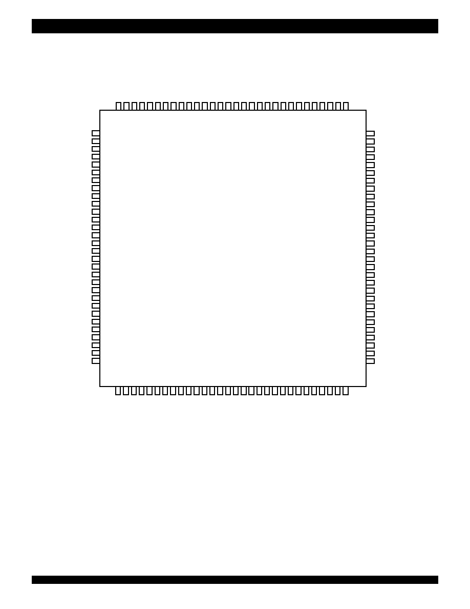
PIN CONFIGURATION (Continued)
TQFP (PN120-1, order code: PF)
TOP VIEW
NOTE:
1. NC ≠ No internal connection
B
35
B
34
B
33
B
32
GND
B
31
B
30
B
29
B
28
B
27
B
26
V
CC
B
25
B
24
GND
B
23
B
22
B
21
B
20
B
19
B
18
GND
B
17
B
16
V
CC
B
15
B
14
B
13
B
12
GND
A
35
A
34
A
33
A
32
V
CC
A
31
A
30
GND
A
29
A
28
A
27
A
26
A
25
A
24
A
23
GND
A
22
V
CC
A
21
A
20
A
19
A
18
GND
A
17
A
16
A
15
A
14
A
13
V
CC
A
12
4658 drw 03
1
2
3
4
5
6
7
8
9
10
11
12
13
14
15
16
17
18
19
20
21
22
23
24
25
26
27
28
29
30
90
89
88
87
86
85
84
83
82
81
80
79
78
77
76
75
74
73
72
71
70
69
68
67
66
65
64
63
62
61
91
120
119
118
117
116
115
114
113
112
111
110
109
108
107
106
105
104
103
102
101
100
99
98
97
96
95
94
93
92
31
32
33
34
35
36
37
38
39
40
41
42
43
44
45 46
47
48
49
50
51
52
53
54
55
56
57
58
59
60
GND
CLKA
ENA
W/
R
A
CSA
IR
OR V
CC
AF AE
VCC
MBF2
MBA
RST
GND
FS0/SD
FS1/
SEN
RTM
RFM
V
CC
NC MBB
GND
MBF1
GND
CSB W
/RB
ENB
CLKB
V
CC
B
11
B
9
B
10
B
7
B
8
B
6
B
0
B
1
B
2
B
3
B
4
B
5
GND
V
CC
GND
A
0
A
1
A
3
A
4
A
2
A
5
V
CC
GND
GND
GND
A
11
A
10
A
9
A
8
A
7
A
6
4
Commercial Temperature
IDT72V3631/72V3641/72V3651
3.3V CMOS SYNCFIFOTM 512 x 36, 1,024 x 36 AND 2,048 x 36
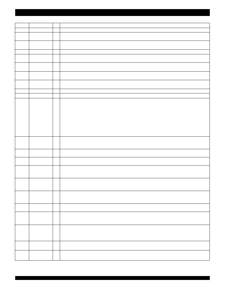
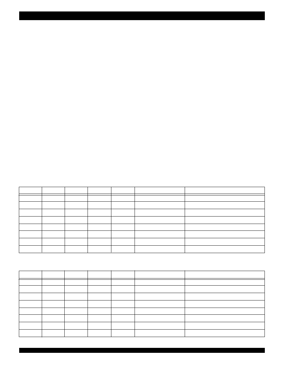
PIN DESCRIPTION
Symbol
Name
I/O
Description
A0-A35
Port-A Data
I/O 36-bit bidirectional data port for side A.
AE
Almost-Empty
O
Programmable flag synchronized to CLKB. It is LOW when the number of words in the FIFO is less than or equal to
Flag
the value in the Almost-Empty register (X).
AF
Almost-Full
O
Programmable flag synchronized to CLKA. It is LOW when the number of empty locations in the FIFO is less than or
Flag
equal to the value in the Almost-Full Offset register (Y).
B0-B35
Port-B Data
I/O 36-bit bidirectional data port for side B.
CLKA
Port-A Clock
I
CLKA is a continuous clock that synchronizes all data transfers through port-A and may be asynchronous or
coincident to CLKB. IR and
AF are synchronous to the LOW-to-HIGH transition of CLKA.
CLKB
Port-B Clock
I
CLKB is a continuous clock that synchronizes all data transfers through port-B and may be asynchronous or
coincident to CLKA. OR and
AE are synchronous to the LOW-to-HIGH transition of CLKB.
CSA
Port-A Chip
I
CSA must be LOW to enable a LOW-to-HIGH transition of CLKA to read or write data on port-A. The A0-A35
Select
outputs are in the high-impedance state when
CSA is HIGH.
CSB
Port-B Chip
I
CSB must be LOW to enable a LOW-to-HIGH transition of CLKB to read or write data on port-B. The B0-B35
Select
outputs are in the high-impedance state when
CSB is HIGH.
ENA
Port-A Enable
I
ENA must be HIGH to enable a LOW-to-HIGH transition of CLKA to read or write data on port-A.
ENB
Port-B Enable
I
ENB must be HIGH to enable a LOW-to-HIGH transition of CLKB to read or write data on port-B.
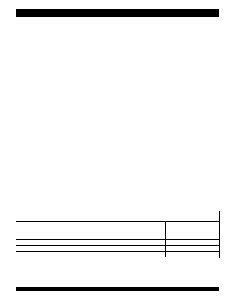
FS1/
Flag-Offset
I
FS1/
SEN and FS0/SD are dual-purpose inputs used for flag Offset register programming. During a device reset,
SEN,
Select 1/
FS1/
SEN and FS0/SD selects the flag offset programming method. Three Offset register programming methods are
Serial Enable
available: automatically load one of two preset values, parallel load from port A, and serial load.
FS0/SD
Flag Offset 0/
When serial load is selected for flag Offset register programming, FS1/
SEN is used as an enable synchronous to
Serial Data
the LOW-to-HIGH transition of CLKA. When FS1/
SEN is LOW, a rising edge on CLKA load the bit present on FS0/
SD into the X and Y registers. The number of bit writes required to program the Offset registers is 18/20/22 for the
IDT72V3631/72V3641/72V3651 respectively. The first bit write stores the Y-register MSB and the last bit write stores
the X-register LSB.
IR
Input Ready
O
IR is synchronized to the LOW-to-HIGH transition of CLKA. When IR is LOW, the FIFO is full and writes to its
Flag
array are disabled. When the FIFO is in retransmit mode, IR indicates when the memory has been filled to the point
of the retransmit data and prevents further writes. IR is set LOW during reset and is set HIGH after reset.
MBA
Port-A Mailbox
I
A HIGH level chooses a mailbox register for a port-A read or write operation.
Select
MBB
Port-B Mailbox
I
A HIGH level chooses a mailbox register for a port-B read or write operation. When the B0-B35 outputs are active,
Select
a HIGH level on MBB selects data from the mail1 register for output and a LOW level selects FIFO data for output.
MBF1
Mail1 Register
O
MBF1 is set LOW by the LOW-to-HIGH transition of CLKA that writes data to the mail1 register. MBF1 is set HIGH
Flag
by a LOW-to-HIGH transition of CLKB when a port-B read is selected and MBB is HIGH.
MBF1 is set HIGH by a
reset.
MBF2
Mail2 Register
O
MBF2 is set LOW by the LOW-to-HIGH transition of CLKB that writes data to the mail2 register. MBF2 is set HIGH
Flag
by a LOW-to-HIGH transition of CLKA when a port-A read is selected and MBA is HIGH.
MBF2 is set HIGH by a
reset.
OR
Output Ready
O
OR is synchronized to the LOW-to-HIGH transition of CLKB. When OR is LOW, the FIFO is empty and reads are
Flag
disabled. Ready data is present in the output register of the FIFO when OR is HIGH. OR is forced LOW during the
reset and goes HIGH on the third LOW-to-HIGH transition of CLKB after a word is loaded to empty memory.
RFM
Read From
I
When the FIFO is in retransmit mode, a HIGH on RFM enables a LOW-to-HIGH transition of CLKB to reset the read
Mark
pointer to the beginning retransmit location and output the first selected retransmit data.
RST
Reset
I
To reset the device, four LOW-to-HIGH transitions of CLKA and four LOW-to-HIGH transitions of CLKB must occur
while
RST is LOW. The LOW-to-HIGH transition of RST latches the status of FS0 and FS1 for AF and AE offset
selection.
RTM
Retransmit
I
When RTM is HIGH and valid data is present in the FIFO output register (OR is HIGH), a LOW-to-HIGH transition
Mode
of CLKB selects the data for the beginning of a retransmit and puts the FIFO in retransmit mode. The selected word
remains the initial retransmit point until a LOW- to-HIGH transition of CLKB occurs while RTM is LOW, taking the FIFO
out of retransmit mode.
W/
RA
Port-A Write/
I
A HIGH selects a write operation and a LOW selects a read operation on port A for a LOW-to-HIGH transition of
Read Select
CLKA. The A0-A35 outputs are in the high-impedance state when W/
RA is HIGH.
W/RB
Port-B Write/
I
A LOW selects a write operation and a HIGH selects a read operation on port B for a LOW-to-HIGH transition of
Read Select
CLKB. The B0-B35 outputs are in the high-impedance state when
W/RB is LOW.
5
Commercial Temperature
IDT72V3631/72V3641/72V3651
3.3V CMOS SYNCFIFOTM 512 x 36, 1,024 x 36 AND 2,048 x 36
ABSOLUTE MAXIMUM RATINGS OVER OPERATING FREE-AIR
TEMPERATURE RANGE (Unless otherwise noted)
(2)
Symbol
Rating
Commercial
Unit
V
CC
Supply Voltage Range
≠0.5 to +4.6
V
V
I
(2)
Input Voltage Range
≠0.5 to V
CC
+0.5
(3)
V
V
O
(2)
Output Voltage Range
≠0.5 to V
CC
+0.5
V
I
IK
Input Clamp Current, (V
I
< 0 or V
I
> V
CC
)
±20
mA
I
OK
Output Clamp Current, (V
O
= < 0 or V
O
> V
CC
)
±50
mA
I
OUT
Continuous Output Current, (V
O
= 0 to V
CC
)
±50
mA
I
CC
Continuous Current Through V
CC
or GND
±400
mA
T
STG
Storage Temperature Range
≠65 to 150
∞
C
IDT72V3631
IDT72V3641
IDT72V3651
Commercial
t
CLK
= 15, 20 ns
Symbol
Parameter
Test Conditions
Min.
Typ.
(1)
Max.
Unit
V
OH
Output Logic "1" Voltage
V
CC
= 3.0V,
I
OH
= ≠4 mA
2.4
--
--
V
V
OL
Output Logic "0" Voltage
V
CC
= 3.0V,
I
OL
= 8 mA
--
--
0.5
V
I
LI
Input Leakage Current (Any Input)
V
CC
= 3.6V,
V
I
= V
CC
or 0
--
--
±5
µ A
I
LO
Output Leakage Current
V
CC
= 3.6V,
V
O
= V
CC
or 0
--
--
±5
µ A
I
CC2
(2)
Standby Current
V
CC
= 3.6V,
V
I
= V
CC
≠0.2V or 0
--
--
400
µ A
C
IN
Input Capacitance
V
I
= 0,
f = 1 MHz
--
4
--
pF
C
OUT
Output Capacitance
V
O
= 0,
f = 1 MHZ
--
8
--
pF
ELECTRICAL CHARACTERISTICS OVER RECOMMENDED OPERATING
FREE-AIR TEMPERATURE RANGE (Unless otherwise noted)
NOTES:
1. All typical values are at V
CC
= 3.3V, T
A
= 25
∞
C.
2. For additional I
CC
information, see Figure 1, Typical Characteristics: Supply Current (I
CC
) vs. Clock Frequency (f
S
).
NOTES:
1. Stresses beyond those listed under "Absolute Maximum Ratings" may cause permanent damage to the device. These are stress ratings only and functional operation of the device at these
or any other conditions beyond those indicated under "Recommended Operating Conditions" is not implied. Exposure to absolute-maximum-rated conditions for extended periods may
affect device reliability.
2. The input and output voltage ratings may be exceeded provided the input and output current ratings are observed.
3. Control Inputs: maximum V
I
= 5.0V.
RECOMMENDED OPERATING
CONDITIONS
Symbol
Parameter
Min.
Typ.
Max.
Unit
V
CC
Supply Voltage
3.0
3.3
3.6
V
V
IH
HIGH Level Input Voltage
2
--
V
CC
+0.5
V
V
IL
LOW-Level Input Voltage
--
--
0.8
V
I
OH
HIGH-Level Output Current
--
--
≠4
mA
I
OL
LOW-Level Output Current
--
--
8
mA
T
A
Operating Free-air
0
--
70
∞
C
Temperature
6
Commercial Temperature
IDT72V3631/72V3641/72V3651
3.3V CMOS SYNCFIFOTM 512 x 36, 1,024 x 36 AND 2,048 x 36
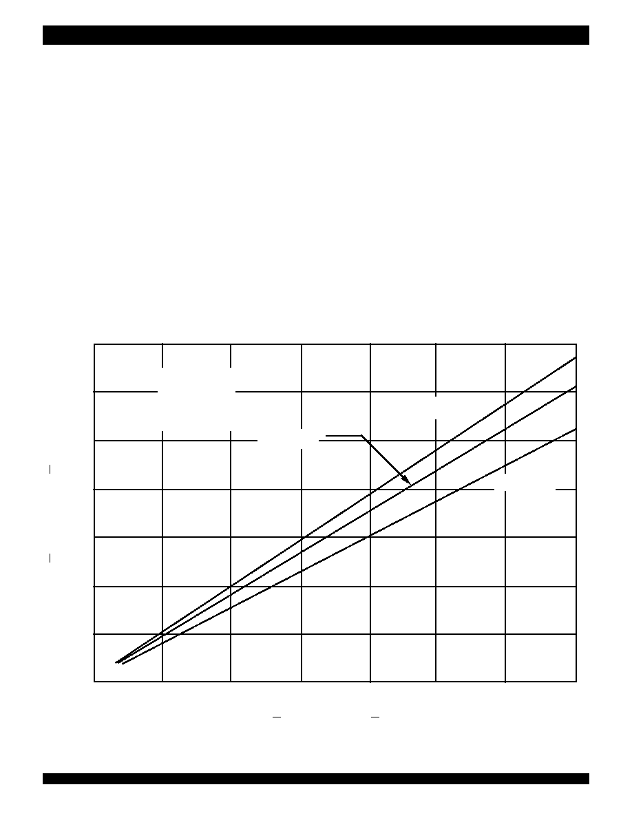
Figure 1. Typical Characteristics: Supply Current (I
CC
) vs. Clock Frequency (f
S
)
DETERMINING ACTIVE CURRENT CONSUMPTION AND POWER DISSIPATION
The I
CC
(f) current for the graph in Figure 1 was taken while simultaneously reading and writing the FIFO on the IDT72V3641 with CLKA and CLKB set
to f
S
. All data inputs and data outputs change state during each clock cycle to consume the highest supply current. Data outputs were disconnected to normalize
the graph to a zero-capacitance load. Once the capacitance load per data-output channel and the number of IDT72V3631/72V3641/72V3651 inputs driven
by TTL HIGH levels are known, the power dissipation can be calculated with the equation below.
CALCULATING POWER DISSIPATION
With I
CC
(f) taken from Figure 1, the maximum power dissipation (PT) of these FIFOs may be calculated by:
P
T
= V
CC
x I
CC(f)
+
(C
L
x V
CC
2
x
f
O
)
N
where:
N = number of outputs = 36
C
L
= output capacitance load
f
O
= switching frequency of an output
When no reads or writes are occurring on these devices, the power dissipated by a single clock (CLKA or CLKB) input running at frequency f
S
is
calculated by:
P
T
= V
CC
x f
S
x 0.025 mA/MHz
0
10
20
30
40
50
60
70
0
25
50
75
100
125
150
V
CC
= 3.3V
f
S
Clock Frequency MHz
I
CC(f)
Supply Current mA
f
data
= 1/2 f
S
T
A
= 25
∞
C
C
L
= 0 pF
V
CC
= 3.0V
V
CC
= 3.6V
4658 drw 04
175
7
Commercial Temperature
IDT72V3631/72V3641/72V3651
3.3V CMOS SYNCFIFOTM 512 x 36, 1,024 x 36 AND 2,048 x 36
AC ELECTRICAL CHARACTERISTICS OVER RECOMMENDED RANGES OF
SUPPLY VOLTAGE AND OPERATING FREE-AIR TEMPERATURE
IDT72V3631L15
IDT72V3631L20
IDT72V3641L15
IDT72V3641L20
IDT72V3651L15
IDT72V3651L20
Symbol
Parameter
Min.
Max.
Min.
Max.
Unit
f
S
Clock Frequency, CLKA or CLKB
≠
66.7
≠
50
MHz
t
CLK
Clock Cycle Time, CLKA or CLKB
15
≠
20
≠
ns
t
CLKH
Pulse Duration, CLKA or CLKB HIGH
6
≠
8
≠
ns
t
CLKL
Pulse Duration, CLKA or CLKB LOW
6
≠
8
≠
ns
t
DS
Setup Time, A0-A35 before CLKA
and B0-B35
5
≠
6
≠
ns
before CLKB
t
ENS1
Setup Time, ENA to CLKA
; ENB to CLKB
5
≠
6
≠
ns
t
ENS2
Setup Time,
CSA, W/RA, and MBA to CLKA
;
7
≠
7.5
≠
ns
CSB, W/RB, and MBB to CLKB
t
RMS
Setup Time, RTM and RFM to CLKB
6
≠
6.5
≠
ns
t
RSTS
Setup Time,
RST LOW before CLKA
5
≠
6
≠
ns
or CLKB
(1)
t
FSS
Setup Time, FS0 and FS1 before
RST HIGH
9
≠
10
≠
ns
t
SDS
(2)
Setup Time, FS0/SD before CLKA
5
≠
6
≠
ns
t
SENS
(2)
Setup Time, FS1/
SEN before CLKA
5
≠
6
≠
ns
t
DH
Hold Time, A0-A35 after CLKA
and B0-B35
0.5
≠
0.5
≠
ns
after CLKB
t
ENH1
Hold Time, ENA after CLKA
; ENB after CLKB
0.5
≠
0.5
≠
ns
t
ENH2
Hold Time,
CSA, W/RA, and MBA after CLKA
;
0.5
≠
0.5
≠
ns
CSB, W/RB, and MBB after CLKB
t
RMH
Hold Time, RTM and RFM after CLKB
0.5
≠
0.5
≠
ns
t
RSTH
Hold Time,
RST LOW after CLKA
or CLKB
(1)
5
≠
6
≠
ns
t
FSH
Hold Time, FS0 and FS1 after
RST HIGH
0
≠
0
≠
ns
t
SPH
(2)
Hold Time, FS1/
SEN HIGH after RST HIGH
0
≠
0
≠
ns
t
SDH
(2)
Hold Time, FS0/SD after CLKA
0
≠
0
≠
ns
t
SENH
(2)
Hold Time, FS1/
SEN after CLKA
0
≠
0
≠
ns
t
SKEW1
(3)
Skew Time, between CLKA
and CLKB
9
≠
11
≠
ns
for OR and IR
t
SKEW2
(3,4)
Skew Time, between CLKA
and CLKB
12
≠
16
≠
ns
for
AE and AF
NOTES:
1. Requirement to count the clock edge as one of at least four needed to reset a FIFO.
2. Only applies when serial load method is used to program flag Offset registers.
3. Skew time is not a timing constraint for proper device operation and is only included to illustrate the timing relationship between CLKA cycle and CLKB cycle.
4. Design simulated, not tested.
8
Commercial Temperature
IDT72V3631/72V3641/72V3651
3.3V CMOS SYNCFIFOTM 512 x 36, 1,024 x 36 AND 2,048 x 36
AC ELECTRICAL CHARACTERISTICS
IDT72V3631L15
IDT72V3631L20
IDT72V3641L15
IDT72V3641L20
IDT72V3651L15
IDT72V3651L20
Symbol
Parameter
Min.
Max.
Min.
Max.
Unit
f
S
Clock Frequency, CLKA or CLKB
≠
66.7
≠
50
MHz
t
A
Access Time, CLKB
to B0-B35
2
10
2
12
ns
t
PIR
Propagation Delay Time, CLKA
to IR
1
8
1
10
ns
t
POR
Propagation Delay Time, CLKB
to OR
1
8
1
10
ns
t
PAE
Propagation Delay Time, CLKB
to
AE
1
8
1
10
ns
t
PAF
Propagation Delay Time, CLKA
to
AF
1
8
1
10
ns
t
PMF
Propagation Delay Time, CLKA
to
MBF1
0
8
0
10
ns
LOW or
MBF2 HIGH and CLKB
to
MBF2
LOW or
MBF1 HIGH
t
PMR
Propagation Delay Time, CLKA
to B0-B35
(1)
2
10
2
12
ns
and CLKB
to A0-A35
(2)
t
MDV
Propagation Delay Time, MBB to B0-B35 Valid
2
10
2
12
ns
t
RSF
Propagation Delay Time,
RST LOW to AE LOW
1
15
1
20
ns
and
AF HIGH
t
EN
Enable Time,
CSA and W/RA LOW to A0-A35
2
10
2
12
ns
Active and
CSB LOW and W/RB HIGH to
B0-B35 Active
t
DIS
Disable Time,
CSA or W/RA HIGH to A0-A35
1
8
1
10
ns
at high impedance and
CSB HIGH or W/RB
LOW to B0-B35 at high impedance
NOTES:
1. Writing data to the mail1 register when the B0-B35 outputs are active and MBB is HIGH.
2. Writing data to the mail2 register when the A0-A35 outputs are active and MBA is HIGH.

9
Commercial Temperature
IDT72V3631/72V3641/72V3651
3.3V CMOS SYNCFIFOTM 512 x 36, 1,024 x 36 AND 2,048 x 36
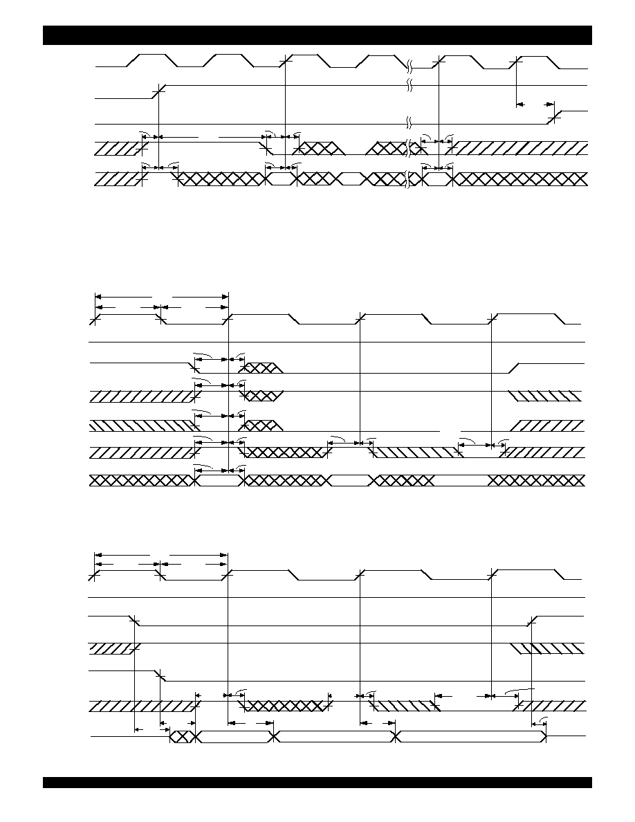
is complete, the X and Y register values are loaded bitwise through the FS0/
SD input on each LOW-to-HIGH transition of CLKA that the FS1/
SEN input is
LOW. There are 18-, 20-, or 22-bit writes needed to complete the programming
for the IDT72V3631, IDT72V3641, or IDT72V3651, respectively. The first-bit
write stores the most significant bit of the Y register, and the last-bit write stores
the least significant bit of the X register. Each register value can be programmed
from 1 to 508 (IDT72V3631), 1 to 1,020 (IDT72V3641), or 1 to 2,044
(IDT72V3651).
When the option to program the Offset registers serially is chosen, the
Input Ready (IR) flag remains LOW until all register bits are written. The IR flag
is set HIGH by the LOW-to-HIGH transition of CLKA after the last bit is loaded
to allow normal FIFO operation. The timing diagram for serial load of offset
registers can be found in Figure 4.
FIFO WRITE/READ OPERATION
The state of the port-A data (A0-A35) outputs is controlled by the port-A
Chip Select (
CSA) and the port-A Write/Read select (W/RA). The A0-A35
outputs are in the high-impedance state when either
CSA or W/RA is HIGH. The
A0-A35 outputs are active when both
CSA and W/RA are LOW.
Data is loaded into the FIFO from the A0-A35 inputs on a LOW-to-HIGH
transition of CLKA when
CSA and the port-A Mailbox select (MBA) are LOW,
W/
RA, the port-A Enable (ENA), and the Input Ready (IR) flag are HIGH (see
Table 2). Writes to the FIFO are independent of any concurrent FIFO read. For
the Write Cycle Timing diagram, see Figure 5.
The port-B control signals are identical to those of port-A with the
exception that the port-B Write/Read select (
W/RB) is the inverse of the port-
A Write/Read select (W/
RA). The state of the port-B data (B0-B35) outputs is
controlled by the port-B Chip Select (
CSB) and the port-B Write/Read select (W/
RB). The B0-B35 outputs are in the high-impedance state when either
CSB is
HIGH or
W/RB is LOW. The B0-B35 outputs are active when CSB is LOW and
W/RB is HIGH.
Data is read from the FIFO to its output register on a LOW-to-HIGH transition
of CLKB when
CSB and the port-B Mailbox select (MBB) are LOW, W/RB, the
port-B Enable (ENB), and the Output Ready (OR) flag are HIGH (see Table 3).
Reads from the FIFO are independent of any concurrent FIFO writes. For the
Read Cycle Timing diagram, see Figure 6.
The setup- and hold-time constraints to the port clocks for the port Chip
Selects and Write/Read selects are only for enabling write and read operations
and are not related to high-impedance control of the data outputs. If a port Enable
is LOW during a clock cycle, the port Chip Select and Write/Read select may
change states during the setup- and hold time window of the cycle.
When the OR flag is LOW, the next data word is sent to the FIFO output
register automatically by the CLKB LOW-to-HIGH transition that sets the
OR flag HIGH. When OR is HIGH, an available data word is clocked to the
FIFO output register only when a FIFO read is selected by the port-B Chip Select
(
CSB), Write/Read select (W/RB), Enable (ENB), and Mailbox select (MBB).
SIGNAL DESCRIPTION
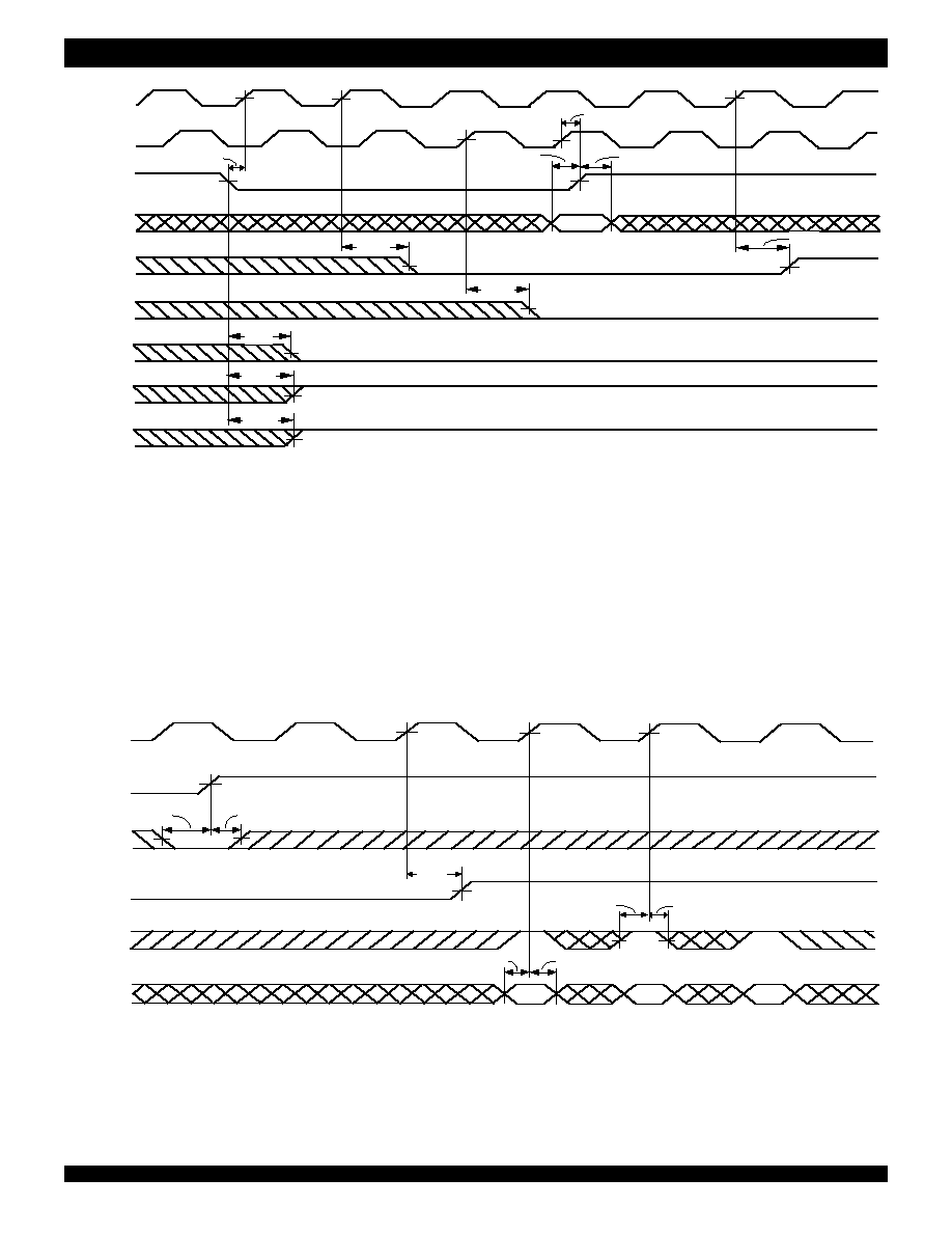
RESET
The IDT72V3631/72V3641/72V3651 is reset by taking the Reset (
RST)
input LOW for at least four port-A Clock (CLKA) and four port-B (CLKB) LOW-
to-HIGH transitions. The Reset input may switch asynchronously to the clocks.
A reset initializes the memory read and write pointers and forces the Input
Ready (IR) flag LOW, the Output Ready (OR) flag LOW, the Almost-Empty (
AE)
flag LOW, and the Almost-Full (
AF) flag HIGH. Resetting the device also forces
the Mailbox Flags (
MBF1, MBF2) HIGH. After a FIFO is reset, its Input Ready
flag is set HIGH after at least two clock cycles to begin normal operation. A FIFO
must be reset after power up before data is written to its memory. The relevant
FIFO Reset timing diagram can be found in Figure 2.
FIRST WORD FALL THROUGH MODE (FWFT)
These devices operate in the First Word Fall Through mode (FWFT). This
mode uses the Output Ready function (OR) to indicate whether or not there is
valid data at the data outputs (B0-B35). It also uses the Input Ready (IR) function
to indicate whether or not the FIFO memory has any free space for writing. In
the FWFT mode, the first word written to an empty FIFO goes directly to data
outputs, no read request necessary. Subsequent words must be accessed by
performing a formal read operation.
ALMOST-EMPTY FLAG AND ALMOST-FULL FLAG OFFSET PRO-
GRAMMING
Two registers in these devices are used to hold the offset values for the
Almost-Empty and Almost-Full flags. The Almost-Empty (
AE) flag Offset
register is labeled X, and the Almost-Full (
AF) flag Offset register is labeled Y.
The Offset register can be loaded with a value in three ways: one of two preset
values are loaded into the Offset registers, parallel load from port A, or serial
load. The Offset register programming mode is chosen by the flag select (FS1,
FS0) inputs during a LOW-to-HIGH transition on the
RST input (See Table 1).
--
PRESET VALUES
If the preset value of 8 or 64 is chosen by the FS1 and FS0 inputs at the
time of a
RST LOW-to-HIGH transition according to Table 1, the preset value
is automatically loaded into the X and Y registers. No other device initialization
is necessary to begin normal operation, and the IR flag is set HIGH after two
LOW-to-HIGH transitions on CLKA. For the Preset value loading timing
diagram, see Figure 2.
--
PARALLEL LOAD FROM PORT A
To program the X and Y registers from port A, the device is reset with FS0
and FS1 LOW during the LOW-to-HIGH transition of
RST. After this reset is
complete, the IR flag is set HIGH after two LOW-to-HIGH transitions on CLKA.
The first two writes to the FIFO do not store data in its memory but load the Offset
registers in the order Y, X. Each Offset register of the IDT72V3631, IDT72V3641,
and IDT72V3651 uses port-A inputs (A8-A0), (A9-A0), and (A10-A0), respec-
tively. The highest number input is used as the most significant bit of the binary
number in each case. Each register value can be programmed from 1 to 508
(IDT72V3631), 1 to 1,020 (IDT72V3641), and 1 to 2,044 (IDT72V3651). After
both Offset registers are programmed from port A, subsequent FIFO writes
store data in the RAM. The timing diagram for parallel load of offset registers
can be found in Figure 3.
--
SERIAL LOAD
To program the X and Y registers serially, the device is reset with FS0/SD
and FS1/
SEN HIGH during the LOW-to-HIGH transition of RST. After this reset
NOTE:
1. X register holds the offset for
AE; Y register holds the offset for AF.
FS1
FS0
RST
X and Y Registers
(1)
H
H
Serial Load
H
L
64
L
H
8
L
L
Parallel Load From Port A
Table 1. Flag Programming
10
Commercial Temperature
IDT72V3631/72V3641/72V3651
3.3V CMOS SYNCFIFOTM 512 x 36, 1,024 x 36 AND 2,048 x 36
SYNCHRONIZED FIFO FLAGS
Each IDT72V3631/72V3641/72V3651 FIFO flag is synchronized to its
port Clock through at least two flip-flop stages. This is done to improve the flags'
reliability by reducing the probability of metastable events on their outputs when
CLKA and CLKB operate asynchronously to one another. OR and
AE are
synchronized to CLKB. IR and
AF are synchronized to CLKA. Table 4 shows
the relationship of each flag to the number of words stored in memory.
OUTPUT READY FLAG (OR)
The Output Ready flag of a FIFO is synchronized to the port Clock that
reads data from its array (CLKB). When the OR flag is HIGH, new data is present
in the FIFO output register. When the OR flag is LOW, the previous data word
is present in the FIFO output register and attempted FIFO reads are ignored.
A FIFO read pointer is incremented each time a new word is clocked to
its output register. The state machine that controls an OR flag monitors a write-
pointer and read-pointer comparator that indicates when the FIFO memory
status is empty, empty+1, or empty+2. From the time a word is written to a FIFO,
it can be shifted to the FIFO output register in a minimum of three cycles of CLKB.
Therefore, an OR flag is LOW if a word in memory is the next data to be sent
to the FIFO output register and three CLKB cycles have not elapsed since the
time the word was written. The OR flag of the FIFO remains LOW until the third
LOW-to-HIGH transition of CLKB occurs, simultaneously forcing the OR flag
HIGH and shifting the word to the FIFO output register.
A LOW-to-HIGH transition on CLKB begins the first synchronization cycle
of a write if the clock transition occurs at time t
SKEW1
or greater after the write.
Otherwise, the subsequent CLKB cycle may be the first synchronization cycle
(see Figure 7).
INPUT READY FLAG (IR)
The Input Ready flag of a FIFO is synchronized to the port Clock that writes
data to its array (CLKA). When the IR flag is HIGH, a memory location is free
in the FIFO to write new data. No memory locations are free when the IR flag
is LOW and attempted writes to the FIFO are ignored.
Each time a word is written to a FIFO, its write pointer is incremented. The
state machine that controls an IR flag monitors a write-pointer and read pointer
comparator that indicates when the FIFO memory status is full, full-1, or full-2.
From the time a word is read from a FIFO, its previous memory location is ready
to be written in a minimum of three cycles of CLKA. Therefore, an IR flag is LOW
if less than two cycles of CLKA have elapsed since the next memory write location
has been read. The second LOW-to-HIGH transition on CLKA after the read
sets the Input Ready flag HIGH, and data can be written in the following cycle.
A LOW-to-HIGH transition on CLKA begins the first synchronization cycle
of a read if the clock transition occurs at time t
SKEW1
or greater after the read.
Otherwise, the subsequent CLKA cycle may be the first synchronization cycle
(see Figure 8).
ALMOST-EMPTY FLAG (
AE)
The Almost-Empty flag of a FIFO is synchronized to the port Clock that
reads data from its array (CLKB). The state machine that controls an
AE flag
monitors a write-pointer and read-pointer comparator that indicates when the
FIFO memory status is almost-empty, almost-empty+1, or almost-empty+2. The
almost-empty state is defined by the contents of register X. This register is loaded
with a preset value during a FIFO reset, programmed from port A, or
programmed serially (see Almost-Empty flag and Almost-Full flag offset pro-
gramming section). The
AE flag is LOW when the FIFO contains X or less words
Table 3. Port-B Enable Function Table
CSB
W/RB
ENB
MBB
CLKB
Data B (B0-A35) I/O
Port Functions
H
X
X
X
X
Input
None
L
L
L
X
X
Input
None
L
L
H
L
Input
None
L
L
H
H
Input
Mail2 Write
L
H
L
L
X
Output
None
L
H
H
L
Output
FIFO read
L
H
L
H
X
Output
None
L
H
H
H
Output
Mail1 Read (Set
MBF1 HIGH)
Table 2. Port-A Enable Function Table
CSA
W/
RA
ENA
MBA
CLKA
Data A (A0-A35) I/O
Port Functions
H
X
X
X
X
Input
None
L
H
L
X
X
Input
None
L
H
H
L
Input
FIFO Write
L
H
H
H
Input
Mail1 Write
L
L
L
L
X
Output
None
L
L
H
L
Output
None
L
L
L
H
X
Output
None
L
L
H
H
Output
Mail2 Read (Set
MBF2 HIGH)
11
Commercial Temperature
IDT72V3631/72V3641/72V3651
3.3V CMOS SYNCFIFOTM 512 x 36, 1,024 x 36 AND 2,048 x 36
retransmit mode to select a beginning word and prevent ongoing FIFO write
operations from destroying retransmit data. Data vectors with a minimum length
of three words can retransmit repeatedly starting at the selected word. The FIFO
can be taken out of retransmit mode at any time and allow normal device
operation.
The FIFO is put in retransmit mode by a LOW-to-HIGH transition on CLKB
when the retransmit mode (RTM) input is HIGH and OR is HIGH. The rising
CLKB edge marks the data present in the FIFO output register as the first
retransmit data. The FIFO remains in retransmit mode until a LOW-to-HIGH
transition occurs while RTM is LOW.
When two or more reads have been done past the initial marked retransmit
word, a retransmit is initiated by a LOW-to-HIGH transition on CLKB when the
read-from-mark (RFM) input is HIGH. This rising CLKB edge shifts the first
retransmit word to the FIFO output register and subsequent reads can begin
immediately. Retransmit loops can be done endlessly while the FIFO is in
retransmit mode. RFM must be LOW during the CLKB rising edge that takes
the FIFO out of retransmit mode (see Figure 11).
When the FIFO is put into retransmit mode, it operates with two read
pointers. The current read pointer operates normally, incrementing each time
when a new word is shifted to the FIFO output register. This read pointer position
is used by the OR and
AE flags. The shadow read pointer stores the memory
location at the time the device is put into retransmit mode and does not change
until the device is taken out of retransmit mode. The shadow read pointer position
is used by the IR and
AF flags. Data writes can proceed while the FIFO is in
retransmit mode, but
AF is set LOW by the write that stores (512-Y), (1,024 - Y),
or (2,048-Y) words after the first retransmit word for the IDT72V3631,
IDT72V3641, or IDT72V3651, respectively. The IR flag is set LOW by the
512th, 1,024th, or 2,048th write after the first retransmit word for the IDT72V3631,
IDT72V3641, or IDT72V3651, respectively.
When the FIFO is in retransmit mode and RFM is HIGH, a rising CLKB
edge loads the current read pointer with the shadow read-pointer value and
the OR flag reflects the new level of fill immediately. If the retransmit changes
the FIFO status out of the almost-empty range, up to two CLKB rising edges after
the retransmit cycle are needed to switch
AE high (see Figure 12). The rising
CLKB edge that takes the FIFO out of retransmit mode shifts the read pointer
used by the IR and
AF flags from the shadow to the current read pointer. If the
change of read pointer used by IR and
AF should cause one or both flags to
transmit HIGH, at least two CLKA synchronizing cycles are needed before the
flags reflect the change. A rising CLKA edge after the FIFO is taken out of
retransmit mode is the first synchronizing cycle of IR if it occurs at time t
SKEW1
or greater after the rising CLKB edge (see Figure 13). A rising CLKA edge after
NOTES:
1. When a word is present in the FIFO output register, its previous memory location is free.
2. Data in the output register does not count as a "word i n FIFO memory". Since in FWFT mode, the first words written to an empty FIFO goes unrequested to the output register (no read
operation necessary), it is not included in the memory count.
3. X is the Almost-Empty Offset for
AE. Y is the Almost-Full Offset for AF.
Table 4. FIFO Flag Operation
and is HIGH when the FIFO contains (X+1) or more words. A data word present
in the FIFO output register has been read from memory.
Two LOW-to-HIGH transitions of CLKB are required after a FIFO write for
the
AE flag to reflect the new level of fill; therefore, the AE flag of a FIFO
containing (X+1) or more words remains LOW if two cycles of CLKB have not
elapsed since the write that filled the memory to the (X+1) level. An
AE flag is
set HIGH by the second LOW-to-HIGH transition of CLKB after the FIFO write
that fills memory to the (X+1) level. A LOW-to-HIGH transition of CLKB begins
the first synchronization cycle if it occurs at time t
SKEW2
or greater after the write
that fills the FIFO to (X+1) words. Otherwise, the subsequent CLKB cycle may
be the first synchronization cycle (see Figure 9).
ALMOST-FULL FLAG (
AF)
The Almost-Full flag of a FIFO is synchronized to the port Clock that writes
data to its array (CLKA). The state machine that controls an
AF flag monitors
a write-pointer and read-pointer comparator that indicates when the FIFO
memory status is almost-full, almost-full-1, or almost-full-2. The almost-full state
is defined by the contents of register Y. This register is loaded with a preset value
during a FIFO reset, programmed from port A, or programmed serially (see
Almost-Empty flag and Almost-Full flag offset programming section). The
AF
flag is LOW when the number of words in the FIFO is greater than or equal to
(512-Y), (1,024-Y), OR (2,048-Y) for the IDT72V3631, IDT72V3641, or
IDT72V3651, respectively. The
AF flag is HIGH when the number of words
in the FIFO is less than or equal to [512-(Y+1)], [1,024-(Y+1)], or [2,048-(Y+1)]
for the IDT72V3631, IDT72V3641, or IDT72V3651, respectively. A data word
present in the FIFO output register has been read from memory.
Two LOW-to-HIGH transitions of CLKA are required after a FIFO read for
its
AF flag to reflect the new level of fill. Therefore, the AF flag of a FIFO
containing [512/1,024/2,048-(Y+1)] or less words remains LOW if two cycles
of CLKA have not elapsed since the read that reduced the number of words in
memory to [512/1,024/2,048-(Y+1)]. An
AF flag is set HIGH by the second
LOW-to-HIGH transition of CLKA after the FIFO read that reduces the number
of words in memory to [512/1,024/2,048-(Y+1)]. A LOW-to-HIGH transition of
CLKA begins the first synchronization cycle if it occurs at time t
SKEW2
or greater
after the read that reduces the number of words in memory to
[512/1,024/2,048-(Y+1)]. Otherwise, the subsequent CLKA cycle may be the
first synchronization cycle (see Figure 10).
SYNCHRONOUS RETRANSMIT
The synchronous retransmit feature of these devices allow FIFO data to
be read repeatedly starting at a user-selected position. The FIFO is first put into
Number of Words in the FIFO
(1,2)
Synchronized
Synchronized
to CLKB
to CLKA
IDT72V3631
(3)
IDT72V3641
(3)
IDT72V3651
(3)
OR
AE
AF
IR
0
0
0
L
L
H
H
1 to X
1 to X
1 to X
H
L
H
H
(X+1) to [512-(Y+1)]
(X+1) to [1,024-(Y+1)]
(X+1) to [2,048-(Y+1)]
H
H
H
H
(512-Y) to 511
(1,024-Y) to 1,023
(2,048-Y) to 2,047
H
H
L
H
512
1,024
2,048
H
H
L
L

12
Commercial Temperature
IDT72V3631/72V3641/72V3651
3.3V CMOS SYNCFIFOTM 512 x 36, 1,024 x 36 AND 2,048 x 36
the FIFO is taken out of retransmit mode is the first synchronizing cycle of
AF
if it occurs at time t
SKEW2
or greater after the rising CLKB edge (see Figure 14).
MAILBOX REGISTERS
Two 36-bit bypass registers are on the IDT72V3631/72V3641/72V3651
to pass command and control information between port A and port B. The
Mailbox select (MBA, MBB) inputs choose between a mail register and a FIFO
for a port data transfer operation. A LOW-to-HIGH transition on CLKA writes
A0-A35 data to the mail1 register when a port-A Write is selected by
CSA, W/
RA, and ENA with MBA HIGH. A LOW-to-HIGH transition on CLKB writes B0-
B35 data to the mail2 register when a port-B Write is selected by
CSB, W/RB,
and ENB with MBB HIGH. Writing data to a mail register sets its corresponding
flag (
MBF1 or MBF2) LOW. Attempted writes to a mail register are ignored
while its mail flag is LOW.
When the port-B data (B0-B35) outputs are active, the data on the bus
comes from the FIFO output register when the port-B Mailbox select (MBB) input
is LOW and from the Mail1 register when MBB is HIGH. Mail2 data is always
present on the port-A data (A0-A35) outputs when they are active. The Mail1
register Flag (
MBF1) is set HIGH by a LOW-to-HIGH transition on CLKB when
a port-B Read is selected by
CSB, W/RB, and ENB with MBB HIGH. The
Mail2 register Flag (MBF2) is set HIGH by a LOW-to-HIGH transition on CLKA
when a port-A Read is selected by
CSA, W/RA, and ENA with MBA HIGH.
The data in a mail register remains intact after it is read and changes only when
new data is written to the register. Mail Register and Mail Register Flag timing
can be found in Figure 15 and 16.
13
Commercial Temperature
IDT72V3631/72V3641/72V3651
3.3V CMOS SYNCFIFOTM 512 x 36, 1,024 x 36 AND 2,048 x 36
Figure 3. Programming the Almost-Full Flag and Almost-Empty Flag Offset Values from Port A
NOTE:
1.
CSA = LOW, W/RA = HIGH, MBA = LOW. It is not necessary to program Offset register on consecutive clock cycles.
Figure 2. FIFO Reset and Loading X and Y with a Preset Value of Eight
CLKA
RST
IR
AE
AF
MBF1
,
MBF2
CLKB
OR
FS1,FS0
4658 drw 05
t
RSTS
t
RSTH
t
FSH
t
FSS
t
PIR
0,1
t
RSF
t
POR
t
RSF
t
RSF
t
PIR
4658 drw 06
CLKA
RST
IR
A0 - A35
FS1,FS0
ENA
t
ENH1
t
ENS1
4
t
PIR
First Word
Stored in FIFO
AE
Offset
(X)
AF
Offset
(Y)
t
FSS
t
FSH
t
DS
t
DH
14
Commercial Temperature
IDT72V3631/72V3641/72V3651
3.3V CMOS SYNCFIFOTM 512 x 36, 1,024 x 36 AND 2,048 x 36
Figure 4. Programming the Almost-Full Flag and Almost-Empty Flag Offset Values Serially
Figure 6. FIFO Read Cycle Timing
NOTE:
1. It is not necessary to program Offset register bits on consecutive clock cycles. FIFO write attempts are ignored until IR is set HIGH.
Figure 5. FIFO Write Cycle Timing
CLKA
RST
IR
FS1/
SEN
FS0/SD
4
AF
Offset
(Y) MSB
AE
Offset
(X) LSB
4658 drw 07
t
FSS
t
FSS
t
FSH
t
SPH
t
SENS
t
SENH
t
SDS
t
SDH
t
SENS
t
SENH
t
SDS
t
SDH
t
PIR
CLKA
IR
ENA
MBA
CSA
W/
R
A
t
CLKH
t
CLKL
t
CLK
t
ENS2
t
ENS2
t
ENS2
t
ENS1
t
ENH2
t
ENH2
t
ENH2
t
ENH1
t
ENS1
t
ENH1
t
ENH1
t
ENS1
4658 drw 08
A0 - A35
t
DS
t
DH
W1
W2
No Operation
HIGH
4658 drw 09
CLKB
OR
ENB
B0 - B35
MBB
CSB
W
/RB
t
CLK
t
CLKH
t
CLKL
t
ENS1
t
A
t
MDV
t
EN
t
A
t
ENS1
t
ENH1
t
ENS1
t
ENH1
W1
W2
W3
t
ENH1
t
DIS
No Operation
HIGH
15
Commercial Temperature
IDT72V3631/72V3641/72V3651
3.3V CMOS SYNCFIFOTM 512 x 36, 1,024 x 36 AND 2,048 x 36
Figure 7. OR Flag Timing and First Data Word Fall Through when the FIFO is Empty
NOTE:
1. t
SKEW1
is the minimum time between a rising CLKA edge and a rising CLKB edge for OR to transition HIGH and to clock the next word to the FIFO output register in three CLKB cycles.
If the time between the rising CLKA edge and rising CLKB edge is less than t
SKEW1
, then the transition of OR HIGH and the first word load to the output register may occur one CLKB cycle
later than shown.
CSA
W/
R
A
MBA
IR
A0 - A35
CLKB
OR
CSB
W
/RB
MBB
ENA
ENB
B0 -B35
CLKA
1
2
3
4658 drw 10
t
CLKH
t
CLKL
t
CLK
t
ENS2
t
ENS1
t
ENH2
t
ENH1
t
DS
t
DH
t
SKEW1
t
CLK
t
CLKL
t
POR
t
POR
t
ENS1
t
ENH1
t
A
Old Data in FIFO Output Register
W1
FIFO Empty
LOW
HIGH
LOW
HIGH
LOW
t
CLKH
W1
HIGH
(1)
16
Commercial Temperature
IDT72V3631/72V3641/72V3651
3.3V CMOS SYNCFIFOTM 512 x 36, 1,024 x 36 AND 2,048 x 36
Figure 9. Timing for
AE when FIFO is Almost-Empty
Figure 8. IR Flag Timing and First Available Write when the FIFO is Full
NOTE:
1. t
SKEW1
is the minimum time between a rising CLKB edge and a rising CLKA edge for IR to transition HIGH in the next CLKA cycle. If the time between the rising CLKB edge and rising
CLKA edge is less than t
SKEW1
, then IR may transition HIGH one CLKA cycle later than shown.
NOTES:
1. t
SKEW2
is the minimum time between a rising CLKA edge and a rising CLKB edge for
AE to transition HIGH in the next CLKB cycle. If the time between the rising CLKA edge and rising
CLKB edge is less than t
SKEW2
, then
AE may transition HIGH one CLKB cycle later than shown.
2. FIFO write (
CSA = LOW, W/RA = HIGH, MBA = LOW), FIFO read (CSB = LOW, W/RB = HIGH, MBB = LOW).
CSB
OR
W
/RB
MBB
ENB
B0 - B35
CLKB
IR
CLKA
CSA
W/
R
A
A0 - A35
MBA
ENA
4658 drw 11
1
2
t
CLK
t
CLKH
t
CLKL
t
ENS1
t
ENH1
t
A
t
SKEW1
t
CLK
t
CLKH
t
CLKL
t
PIR
t
PIR
t
ENS2
t
ENS1
t
DS
t
ENH2
t
ENH1
t
DH
Previous Word in FIFO Output Register
Next Word From FIFO
LOW
HIGH
LOW
HIGH
LOW
HIGH
(1)
FIFO Full
Write
AE
CLKA
ENB
ENA
CLKB
4658 drw 12
2
1
t
ENS1
t
ENH1
t
SKEW2
t
PAE
t
PAE
t
ENS1
t
ENH1
X Word in FIFO
(X+1) Words in FIFO
(1)
17
Commercial Temperature
IDT72V3631/72V3641/72V3651
3.3V CMOS SYNCFIFOTM 512 x 36, 1,024 x 36 AND 2,048 x 36
NOTES:
1. t
SKEW2
is the minimum time between a rising CLKA edge and a rising CLKB edge for
AF to transition HIGH in the next CLKA cycle. If the time between the rising CLKB edge and rising
CLKA edge is less than t
SKEW2
, then
AF may transition HIGH one CLKA cycle later than shown.
2. Depth is 512 for the IDT72V3631, 1,024 for the IDT72V3641, and 2,048 for the IDT72V3651.
3. FIFO write (
CSA = LOW, W/RA = HIGH, MBA = LOW), FIFO read (CSB = LOW, W/RB = HIGH, MBB = LOW).
Figure 10. Timing for
AF when FIFO is Almost-Full
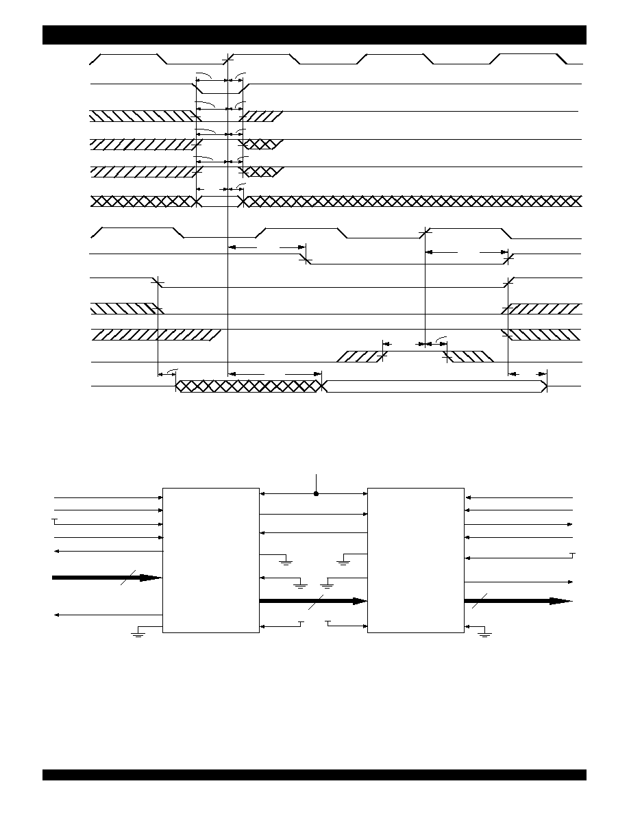
Figure 12.
AE Maximum Latency When Retransmit Increases the Number of Stored Words Above X.
NOTE:
1. X is the value loaded in the Almost-Empty flag Offset register.
NOTE:
1. CSB = LOW, W/RB = HIGH, MBB = LOW. No input enables other than RTM and RFM are needed to control retransmit mode or begin a retransmit. Other enables are shown only to relate
retransmit operations to the FIFO output register.
Figure 11. Retransmit Timing Showing Minimum Retransmit Length
AF
CLKA
ENB
ENA
CLKB
4658 drw 13
1
2
t
SKEW2
t
ENS1
t
ENH1
t
PAF
t
ENS1
t
ENH1
t
PAF
(1)
[Depth -(Y+1)] Words in FIFO
(2)
(Depth -Y) Words in FIFO
(2)
CLKB
ENB
RTM
RFM
OR
B0-B35
W0
W1
W2
W0
W1
HIGH
t
A
t
A
t
A
t
A
Initiate Retransmit Mode
with W0 as First Word
Retransmit from
Selected Position
End Retransmit
Mode
4658 drw 14
t
ENS1
t
ENH1
t
RMS
t
RMH
t
RMS
t
RMH
t
RMS
t
RMH
CLKB
RTM
RFM
AE
t
PAE
X or fewer words from Empty
(X+1) or more
words from Empty
4658 drw 15
t
RMS
t
RMH
1
2
HIGH
18
Commercial Temperature
IDT72V3631/72V3641/72V3651
3.3V CMOS SYNCFIFOTM 512 x 36, 1,024 x 36 AND 2,048 x 36
NOTE:
1. t
SKEW1
is the minimum time between a rising CLKB edge and a rising CLKA edge for IR to transition HIGH in the next CLKA cycle. If the time between the rising CLKB edge and rising
CLKA edge is less than t
SKEW1
, then IR may transition HIGH one CLKA cycle later than shown.
Figure 13. IR Timing from the End of Retransmit Mode when One or More Write Locations are Available
NOTES:
1. t
SKEW2
is the minimum time between a rising CLKB edge and a rising CLKA edge for
AF to transition HIGH in the next CLKA cycle. If the time between the rising CLKB edge and rising
CLKA edge is less than t
SKEW2
, then
AF may transition HIGH one CLKA cycle later than shown.
2. Depth is 512 for the IDT72V3631, 1,024 for the IDT72V3641, and 2,048 for the IDT72V3651.
3. Y is the value loaded in the Almost-Full flag Offset register.
Figure 14.
AF Timing from the End of Retransmit Mode when (Y+1) or More Write Locations are Available
Figure 15. Timing for Mail1 Register and
MBF1 Flag
t
SKEW1
CLKA
IR
CLKB
RTM
FIFO Filled to First Restransmit Word
1
2
One or More Write Locations Available
4658 drw 16
(1)
t
PIR
t
RMS
t
RMH
CLKA
AF
CLKB
RTM
t
SKEW2
(Depth -Y) or More Words Past First Restransmit Word
1
2
(Y+1) or More Write Locations Available
4658 drw 17
(1)
t
PAE
t
RMS
t
RMH
(2)
4658 drw 18
CLKA
ENA
A0 - A35
MBA
CSA
W/
R
A
CLKB
MBF1
CSB
MBB
ENB
B0 - B35
W
/RB
W1
t
ENS2
t
ENH2
t
DS
t
DH
t
PMF
t
PMF
t
EN
t
MDV
t
PMR
t
ENS1
t
ENH1
t
DIS
W1 (Remains valid in Mail1 Register after read)
FIFO Output Register
t
ENS2
t
ENH2
t
ENS2
t
ENH2
t
ENS2
t
ENH2
19
Commercial Temperature
IDT72V3631/72V3641/72V3651
3.3V CMOS SYNCFIFOTM 512 x 36, 1,024 x 36 AND 2,048 x 36
Figure 16. Timing for
Mail2 Register and MBF2 Flag
Figure 17. Block Diagram of 512 x 36, 1,024 x 36, 2,048 x 36 Synchronous FIFO Memory with
Programmable Flags used in Depth Expansion Configuration
NOTES:
1. Mailbox feature is not supported in depth expansion applications. (MBA + MBB tie to GND)
2. Transfer clock should be set either to the Write Port Clock (CLKA) or the Read Port Clock (CLKB), whichever is faster.
3. Retransmit feature is not supported in depth expansion applications.
4. The amount of time it takes for OR of the last FIFO in the chain to go HIGH (i.e. valid data to appear on the last FIFO's outputs) after a word has been written to the first FIFO is the sum
of the delays for each individual FIFO: (N - 1)*(4*transfer clock) + 3*T
RCLK
, where N is the number of FIFOs in the expansion and T
RCLK
is the CLKB period.
5. The amount of time is takes for IR of the first FIFO in the chain to go HIGH after a word has been read from the last FIFO is the sum of the delays for each individual FIFO: (N -
1)*(3*transfer clock) + 2*T
WCLK
, where N is the number of FIFOs in the expansion and T
WCLK
is the CLKA period.
4658 drw 19
CLKB
ENB
B0 - B35
MBB
CSB
W
/RB
CLKA
MBF2
CSA
MBA
ENA
A0 - A35
W/
R
A
W1
t
ENS2
t
ENH2
t
DS
t
DH
t
PMF
t
PMF
t
ENS1
t
ENH1
t
DIS
t
EN
t
PMR
W1 (Remains valid in Mail2 Register after read)
t
ENS2
t
ENH2
t
ENS2
t
ENH2
t
ENS2
t
ENH2
DATA IN (Dn)
READ CLOCK (CLKB)
READ ENABLE (ENB)
OUTPUT READY (OR)
CHIP SELECT (
CSB
)
DATA OUT (Qn)
TRANSFER CLOCK
4658 drw 20
IDT
72V3631
72V3641
72V3651
V
CC
WRITE
READ
A
0
-A
35
MBA
CHIP SELECT (
CSA
)
WRITE SELECT (W/
R
A)
WRITE ENABLE (ENA)
ALMOST-FULL FLAG (
AF
)
INPUT READY (IR)
WRITE CLOCK (CLKA)
CLKB
OR
ENB
CSB
B
0
-B
35
W/
R
B
MBB
CLKA
ENA
IR
CSA
MBA
A
0
-A
35
W/
R
A
READ SELECT (W/
R
B)
ALMOST-EMPTY FLAG (
AE
)
B
0
-B
35
MBB
n
n
n
Qn
Dn
V
CC
V
CC
V
CC
IDT
72V3631
72V3641
72V3651
20
Commercial Temperature
IDT72V3631/72V3641/72V3651
3.3V CMOS SYNCFIFOTM 512 x 36, 1,024 x 36 AND 2,048 x 36
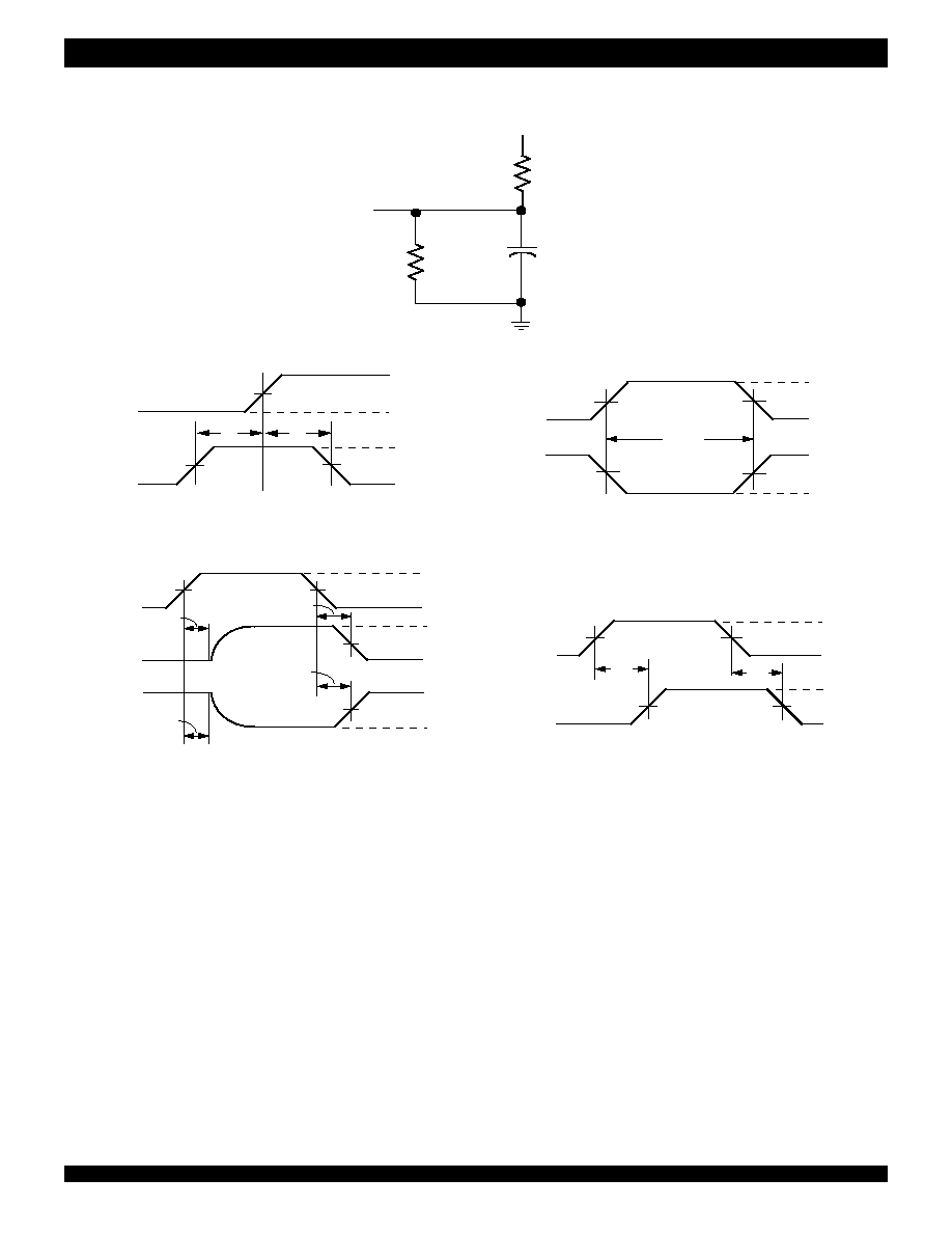
NOTE:
1. Includes probe and jig capacitance
Figure 18. Load Circuit and Voltage Waveforms
4658 drw 21
PARAMETER MEASUREMENT INFORMATION
From Output
Under Test
30 pF
330
3.3V
510
3 V
GND
Timing
Input
Data,
Enable
Input
GND
3 V
1.5 V
1.5 V
VOLTAGE WAVEFORMS
SETUP AND HOLD TIMES
VOLTAGE WAVEFORMS
PULSE DURATIONS
VOLTAGE WAVEFORMS
ENABLE AND DISABLE TIMES
VOLTAGE WAVEFORMS
PROPAGATION DELAY TIMES
3 V
GND
GND
3 V
1.5 V
1.5 V
1.5 V
1.5 V
t
W
Output
Enable
Low-Level
Output
High-Level
Output
3 V
OL
GND
3 V
1.5 V
1.5 V
1.5 V
1.5 V
Ø
OH
OV
Ø
GND
OH
OL
1.5 V
1.5 V
1.5 V
1.5 V
Input
In-Phase
Output
High-Level
Input
Low-Level
Input
V
V
V
V
1.5 V
3 V
t
S
t
h
t
PLZ
t
PHZ
t
PZL
t
PZH
t
PD
t
PD
(1)
21
CORPORATE HEADQUARTERS
for SALES:
for TECH SUPPORT:
2975 Stender Way
800-345-7015 or 408-727-6116
408-330-1753
Santa Clara, CA 95054
fax: 408-492-8674
e-mail: FIFOhelp@idt.com
www.idt.com*
PF Pkg: www.idt.com/docs/PSC4036.pdf
PQF Pkg: www.idt.com/docs/PSC4021.pdf
*To search for sales office near you, please click the sales button found on our home page or dial the 800# above and press 2.
The SyncFIFO is a trademark and the IDT logo is a registered trademark of Integrated Device Technology, Inc.
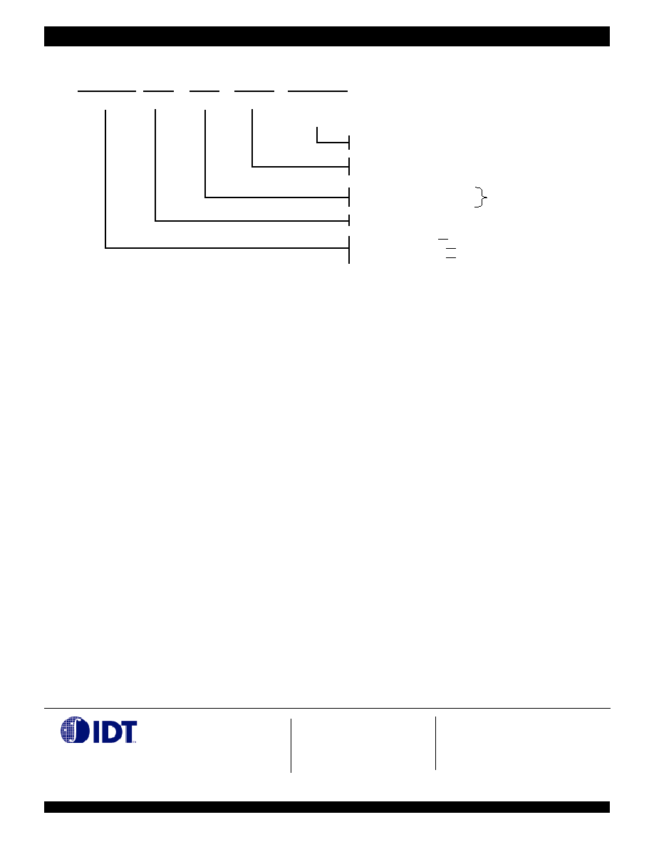
ORDERING INFORMATION
BLANK
PF
PQF
15
20
L
72V3631
72V3641
72V3651
4658 drw 22
Commercial (0
∞
C to +70
∞
C)
Thin Quad Flat Pack (TQFP, PN120-1)
Plastic Quad Flat Pack (PQFP, PQ132-1)
Low Power
512 x 36 3.3V SyncFIFO
1,024 x 36 3.3V SyncFIFO
2,048 x 36 3.3V SyncFIFO
XXXXXX
IDT
Device Type
X
XX
X
X
Power
Speed
Package
Process/
Temperature
Range
Clock Cycle Time (t
CLK
)
Speed in Nanoseconds
Commercial Only
NOTE:
1. Industrial temperature range is available by special order.
DATASHEET DOCUMENT HISTORY
7/31/00
Pgs. 1, 14, 21