 | –≠–ª–µ–∫—Ç—Ä–æ–Ω–Ω—ã–π –∫–æ–º–ø–æ–Ω–µ–Ω—Ç: 72V83 | –°–∫–∞—á–∞—Ç—å:  PDF PDF  ZIP ZIP |
1
1999 Integrated Device Technology, Inc.
DSC-3966/-
©
August 1999
IDT72V81
IDT72V82
IDT72V83
IDT72V84
IDT72V85
3.3 Volt CMOS DUAL ASYNCHRONOUS FIFO
DUAL 512 x 9, DUAL 1,024 x 9
DUAL 2,048 x 9, DUAL 4,096 X 9
DUAL 8,192 X 9
FEATURES:
The IDT72V81 is equivalent to two IDT72V01 - 512 x 9 FIFOs
The IDT72V82 is equivalent to two IDT72V02 - 1,024 x 9 FIFOs
The IDT72V83 is equivalent to two IDT72V03 - 2,048 x 9 FIFOs
The IDT72V84 is equivalent to two IDT72V04 - 4,096 x 9 FIFOs
The IDT72V85 is equivalent to two IDT72V05 - 8,192 x 9 FIFOs
Low power consumption
-- Active: 330 mW (max.)
-- Power-down: 18 mW (max.)
Ultra high speed--15 ns access time
Asynchronous and simultaneous read and write
Offers optimal combination of data capacity, small foot print
and functional flexibility
Ideal for bidirectional, width expansion, depth expansion, bus-
matching, and data sorting applications
Status Flags: Empty, Half-Full, Full
Auto-retransmit capability
High-performance CEMOSTM technology
Space-saving TSSOP package
Industrial temperature range (≠40
∞∞
∞∞
∞
C to +85
∞∞
∞∞
∞
C) is available
DESCRIPTION:
The IDT72V81/72V82/72V83/72V84/72V85 are dual-FIFO memories that
load and empty data on a first-in/first-out basis. These devices are functional and
compatible to two IDT72V01/72V02/72V03/72V04/72V05 FIFOs in a single
package with all associated control, data, and flag lines assigned to separate
pins. The devices use Full and Empty flags to prevent data overflow and
underflow and expansion logic to allow for unlimited expansion capability in both
word size and depth.
The reads and writes are internally sequential through the use of ring
pointers, with no address information required to load and unload data. Data
is toggled in and out of the devices through the use of the Write (
W) and Read
(
R) pins.
The devices utilize a 9-bit wide data array to allow for control and parity
bits at the user's option. This feature is especially useful in data communications
applications where it is necessary to use a parity bit for transmission/reception
error checking. It also features a Retransmit (
RT) capability that allows for reset
of the read pointer to its initial position when
RT is pulsed low to allow for
retransmission from the beginning of data. A Half-Full Flag is available in the
single device mode and width expansion modes.
These FIFOs are fabricated using IDT's high-speed CMOS technology.
They are designed for those applications requiring asynchronous and simul-
taneous read/writes in multiprocessing and rate buffer applications.
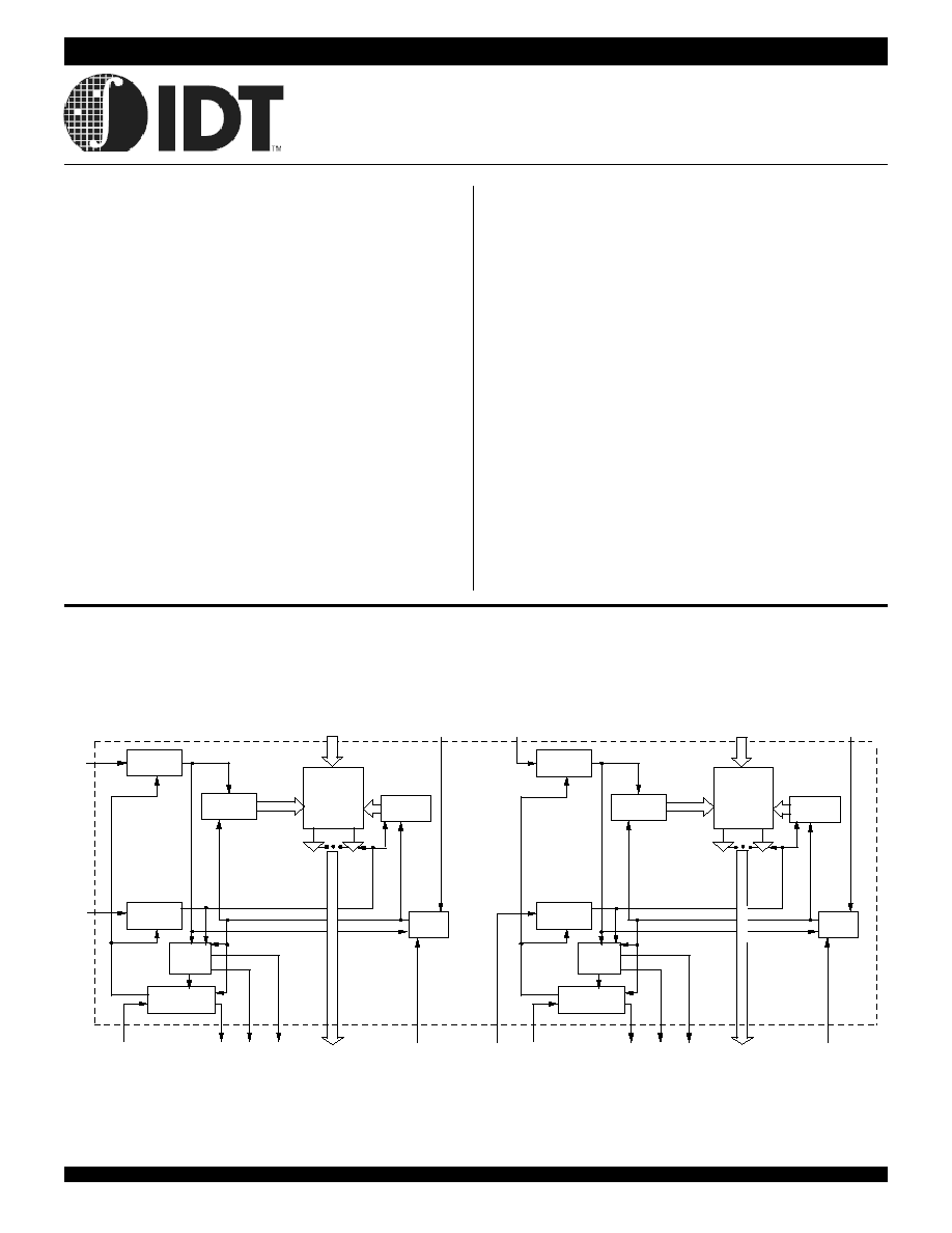
FUNCTIONAL BLOCK DIAGRAM
WA
WRITE
CONTROL
READ
CONTROL
RA
FLAG
LOGIC
EXPANSION
LOGIC
XIA
WRITE
POINTER
RAM
ARRAY A
512 x 9
1,024 x 9
2,048 x 9
4,096 x 9
8,192 x 9
READ
POINTER
DATA INPUTS
RESET
LOGIC
THREE-
STATE
BUFFERS
DATA
OUTPUTS
RSA
FLA
/
RTA
XOA
/
HFA
FFA
EFA
WB
WRITE
CONTROL
READ
CONTROL
RB
FLAG
LOGIC
EXPANSION
LOGIC
XIB
WRITE
POINTER
READ
POINTER
DATA INPUTS
RESET
LOGIC
THREE-
STATE
BUFFERS
DATA
OUTPUTS
RSB
FLB
/
RTB
3966 drw 01
XOB
/
HFB
FFB
EFB
(DA
0
-DA
8
)
(QA
0
-QA
8
)
(QB
0
-QB
8
)
(DB
0
-DB
8
)
RAM
ARRAY A
512 x 9
1,024 x 9
2,048 x 9
4,096 x 9
8,192 x 9
2
Commercial Temperature Range
IDT72V81/72V82/72V83/72V84/72V85
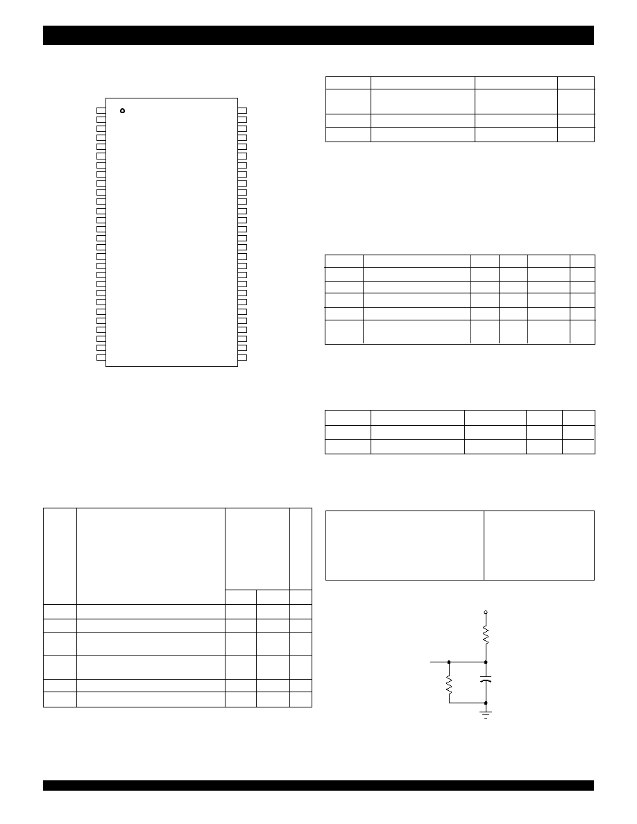
PIN CONFIGURATION
ABSOLUTE MAXIMUM RATINGS
Symbol
Rating
Commercial
Unit
V
TERM
Terminal Voltage
≠0.5 to +7.0
V
with Respect to GND
T
STG
Storage Temperature
≠55 to +125
∞
C
I
OUT
DC Output Current
≠50 to +50
mA
NOTE:
1. Stresses greater than those listed under ABSOLUTE MAXIMUM RATINGS may cause
permanent damage to the device. This is a stress rating only and functional operation of
the device at these or any other conditions above those indicated in the operational
sections of this specification is not implied. Exposure to absolute maximum rating
conditions for extended periods may affect reliability.
Symbol
Parameter
Min.
Typ.
Max.
Unit
V
CC
Supply Voltage
3.0
3.3
3.6
V
GND
Supply Voltage
0
0
0
V
V
IH
(1)
Input High Voltage
2.0
--
V
CC
+0.5
V
V
IL
(2)
Input Low Voltage
--
--
0.8
V
T
A
Operating Temperature
0
--
70
∞
C
Commercial
NOTES:
1. For
RT/RS/XI input, V
IH
= 2.6V (commercial).
2. 1.5V undershoots are allowed for 10ns once per cycle.
RECOMMENDED DC OPERATING
CONDITIONS
AC TEST CONDITIONS
Input Pulse Levels
GND to 3.0V
Input Rise/Fall Times
5ns
Input Timing Reference Levels
1.5V
Output Reference Levels
1.5V
Output Load
See Figure 1
CAPACITANCE
(T
A
= +25
∞
C, f = 1.0 MHz)
Symbol
Parameter
(1)
Condition
Max.
Unit
C
IN
Input Capacitance
V
IN
= 0V
8
pF
C
OUT
Output Capacitance
V
OUT
= 0V
8
pF
NOTE:
1. Characterized values, not currently tested.
NOTES:
1. Measurements with 0.4
V
IN
V
CC
.
2.
R
V
IH
, 0.4
V
OUT
V
CC
.
3. Tested with outputs open (I
OUT
= 0).
4. Tested at f = 20 MHz.
5. All Inputs = V
CC
- 0.2V or GND + 0.2V.
IDT72V81
IDT72V82
IDT72V83
IDT72V84
IDT72V85
Commercial
t
A
= 15, 20 ns
Symbol
Parameter
Min.
Max.
Unit
I
LI
(1)
Input Leakage Current (Any Input)
≠1
1
µ
A
I
LO
(2)
Output Leakage Current
≠10
10
µ
A
V
OH
Output Logic "1" Voltage
2.4
--
V
I
OH
= ≠2mA
V
OL
Output Logic "0" Voltage
--
0.4
V
I
OL
= 8mA
I
CC1
(3,4)
Active Power Supply Current (both FIFOs)
--
100
mA
I
CC2
(3,5)
Standby Current (
R=W=RS=FL/RT=V
IH
)
--
5
mA
FFA
QA
0
QA
1
QA
2
QA
3
QA
8
GND
RA
QA
4
QA
5
QA
6
QA
7
XOA
/
HFA
EFA
FFB
QB
0
QB
1
QB
2
QB
3
QB
8
GND
RB
QB
4
QB
5
QB
6
QB
7
XOB
/
HFB
EFB
1
2
3
4
5
6
7
8
9
10
11
12
13
14
15
16
17
18
19
20
21
22
23
24
25
26
27
28
XIA
DA
0
DA
1
DA
2
DA
3
DA
8
WA
V
CC
DA
4
DA
5
DA
6
DA
7
FLA
/
RTA
RSA
XIB
DB
0
DB
1
DB
2
DB
3
DB
8
WB
V
CC
DB
4
DB
5
DB
6
DB
7
FLB
/
RTB
RSB
56
55
54
53
52
51
50
49
48
47
46
45
44
43
42
41
40
39
38
37
36
35
34
33
32
31
30
29
3966 drw 02
DC ELECTRICAL
CHARACTERISTICS
(1)
(Commercial: V
CC
= 3.3V±0.3V, T
A
= 0
∞
C to +70
∞
C)
3966 drw 03
30pF*
330
3.3V
TO
OUTPUT
PIN
510
or equivalent circuit
Figure 1. Output Load
*Includes scope and jib capacitances.
TSSOP (SO56-2, order code: PA)
TOP VIEW

3
Commercial Temperature Range
IDT72V81/72V82/72V83/72V84/72V85
Commercial
IDT72V81L15
IDT72V81L20
IDT72V82L15
IDT72V82L20
IDT72V83L15
IDT72V83L20
IDT72V84L15
IDT72V84L20
IDT72V85L15
IDT72V85L20
Symbol
Parameter
Min.
Max.
Min.
Max.
Unit
t
S
Shift Frequency
--
40
--
33.3
MHz
t
RC
Read Cycle Time
25
--
30
--
ns
t
A
Access Time
--
15
--
20
ns
t
RR
Read Recovery Time
10
--
10
--
ns
t
RPW
Read Pulse Width
(2)
15
--
20
--
ns
t
RLZ
Read Pulse Low to Data Bus at Low Z
(3)
3
--
3
--
ns
t
WLZ
Write Pulse High to Data Bus at Low Z
(3, 4)
5
--
5
--
ns
t
DV
Data Valid from Read Pulse High
5
--
5
--
ns
t
RHZ
Read Pulse High to Data Bus at High Z
(3)
--
15
--
15
ns
t
WC
Write Cycle Time
25
--
30
--
ns
t
WPW
Write Pulse Width
(2)
15
--
20
--
ns
t
WR
Write Recovery Time
10
--
10
--
ns
t
DS
Data Set-up Time
11
--
12
--
ns
t
DH
Data Hold Time
0
--
0
--
ns
t
RSC
Reset Cycle Time
25
--
30
--
ns
t
RS
Reset Pulse Width
(2)
15
--
20
--
ns
t
RSS
Reset Set-up Time
(3)
15
--
20
--
ns
t
RSR
Reset Recovery Time
10
--
10
--
ns
t
RTC
Retransmit Cycle Time
25
--
30
--
ns
t
RT
Retransmit Pulse Width
(2)
15
--
20
--
ns
t
RTS
Retransmit Set-up Time
(3)
15
--
20
--
ns
t
RTR
Retransmit Recovery Time
10
--
10
--
ns
t
EFL
Reset to Empty Flag Low
--
25
--
30
ns
t
HFH,FFH
Reset to Half-Full and Full Flag High
--
25
--
30
ns
t
RTF
Retransmit Low to Flags Valid
--
25
--
30
ns
t
REF
Read Low to Empty Flag Low
--
15
--
20
ns
t
RFF
Read High to Full Flag High
--
15
--
20
ns
t
RPE
Read Pulse Width after
EF High
15
--
20
--
ns
t
WEF
Write High to Empty Flag High
--
15
--
20
ns
t
WFF
Write Low to Full Flag Low
--
15
--
20
ns
t
WHF
Write Low to Half-Full Flag Low
--
25
--
30
ns
t
RHF
Read High to Half-Full Flag High
--
25
--
30
ns
t
WPF
Write Pulse Width after
FF High
15
--
20
--
ns
t
XOL
Read/Write to
XO Low
--
15
--
20
ns
t
XOH
Read/Write to
XO High
--
15
--
20
ns
t
XI
XI Pulse Width
(2)
15
--
20
--
ns
t
XIR
XI Recovery Time
10
--
10
--
ns
t
XIS
XI Set-up Time
10
--
10
--
ns
NOTES:
1. Timings referenced as in AC Test Conditions.
2. Pulse widths less than minimum value are not allowed.
3. Values guaranteed by design, not currently tested.
4. Only applies to read data flow-through mode.
AC ELECTRICAL CHARACTERISTICS
(1)
(Commercial: V
CC
= 3.3V±0.3V, T
A
= 0
∞
C to +70
∞
C)

4
Commercial Temperature Range
IDT72V81/72V82/72V83/72V84/72V85
Single Device Mode, this pin acts as the retransmit input. The Single Device
Mode is initiated by grounding the Expansion In (
XI).
The IDT72V81/72V82/72V83/72V84/72V85 can be made to retransmit
data when the Retransmit Enable control (
RT) input is pulsed low. A retransmit
operation will set the internal read pointer to the first location and will not affect
the write pointer. Read Enable (
R) and Write Enable (W) must be in the high
state during retransmit for the IDT72V81/72V82/72V83/72V84/72V85 respec-
tively. This feature is useful when less than 512/1,024/2,048/4,096/8,192 writes
are performed between resets. The retransmit feature is not compatible with the
Depth Expansion Mode and will affect the Half-Full Flag (
HF), depending on
the relative locations of the read and write pointers.
EXPANSION IN (
XI
XI
XI
XI
XI )
This input is a dual-purpose pin. Expansion In (
XI) is grounded to indicate
an operation in the single device mode. Expansion In (
XI) is connected to
Expansion Out (
XO) of the previous device in the Depth Expansion or Daisy
Chain Mode.
OUTPUTS:
FULL FLAG (
FF
FF
FF
FF
FF )
The Full Flag (
FF) will go low, inhibiting further write operation, when the write
pointer is one location less than the read pointer, indicating that the device is full.
If the read pointer is not moved after Reset (
RS), the Full-Flag (FF) will go low
after 512 writes for the IDT72V81, 1,024 writes for the IDT72V82, 2,048 writes
for the IDT72V83, 4,096 writes for the IDT72V84 and 8,192 writes for the
IDT72V85.
EMPTY FLAG (
EF
EF
EF
EF
EF )
The Empty Flag (
EF) will go low, inhibiting further read operations, when
the read pointer is equal to the write pointer, indicating that the device is
empty.
EXPANSION OUT/HALF-FULL FLAG (
XO
XO
XO
XO
XO/HF
HF
HF
HF
HF )
This is a dual-purpose output. In the single device mode, when Expan-
sion In (
XI) is grounded, this output acts as an indication of a half-full memory.
After half of the memory is filled and at the falling edge of the next write
operation, the Half-Full Flag (
HF) will be set low and will remain set until the
difference between the write pointer and read pointer is less than or equal
to one half of the total memory of the device. The Half-Full Flag (
HF) is then reset
by using rising edge of the read operation.
In the Depth Expansion Mode, Expansion In (
XI) is connected to Expansion
Out (
XO) of the previous device in the Daisy Chain by providing a pulse to the
next device when the previous device reaches the last location of memory.
DATA OUTPUTS ( Q
0
≠ Q
8
)
Data outputs for 9-bit wide data. This data is in a high impedance
condition whenever Read (
R) is in a high state.
SIGNAL DESCRIPTIONS
INPUTS:
DATA IN (D
0
≠ D
8
)
Data inputs for 9-bit wide data.
CONTROLS:
RESET (
RS
RS
RS
RS
RS )
Reset is accomplished whenever the Reset (
RS) input is taken to a low state.
During reset, both internal read and write pointers are set to the first location.
A reset is required after power up before a write operation can take place. Both
the Read Enable (
R
R
R
R
R ) and Write Enable ( W
W
W
W
W ) inputs must be in the high
state during the window shown in Figure 2, (i.e., t
RSS
before the rising
edge of
RS
RS
RS
RS
RS ) and should not change until t
RSR
after the rising edge of
RS
RS
RS
RS
RS. Half-Full Flag ( HF
HF
HF
HF
HF ) will be reset to high after Reset ( RS
RS
RS
RS
RS ).
WRITE ENABLE (
W
W
W
W
W )
A write cycle is initiated on the falling edge of this input if the Full Flag (
FF)
is not set. Data set-up and hold times must be adhered to with respect to the rising
edge of the Write Enable (
W). Data is stored in the RAM array sequentially and
independently of any on-going read operation.
After half of the memory is filled and at the falling edge of the next write
operation, the Half-Full Flag (
HF) will be set to low and will remain set until the
difference between the write pointer and read pointer is less than or equal to
one half of the total memory of the device. The Half-Full Flag (
HF) is then reset
by the rising edge of the read operation.
To prevent data overflow, the Full Flag (
FF) will go low, inhibiting further write
operations. Upon the completion of a valid read operation, the Full Flag (
FF)
will go high after t
RFF
, allowing a valid write to begin. When the FIFO is full, the
internal write pointer is blocked from
W, so external changes in W will not affect
the FIFO when it is full.
READ ENABLE (
R
R
R
R
R )
A read cycle is initiated on the falling edge of the Read Enable (
R) provided
the Empty Flag (
EF) is not set. The data is accessed on a First-In/First-Out basis,
independent of any ongoing write operations. After Read Enable (
R) goes high,
the Data Outputs (Q
0
≠ Q
8
) will return to a high impedance condition until the
next Read operation. When all data has been read from the FIFO, the Empty
Flag (
EF) will go low, allowing the "final" read cycle but inhibiting further read
operations with the data outputs remaining in a high impedance state. Once a
valid write operation has been accomplished, the Empty Flag (
EF) will go high
after t
WEF
and a valid Read can then begin. When the FIFO is empty, the internal
read pointer is blocked from
R so external changes in R will not affect the FIFO
when it is empty.
FIRST LOAD/RETRANSMIT (
FL
FL
FL
FL
FL/RT
RT
RT
RT
RT )
This is a dual-purpose input. In the Depth Expansion Mode, this pin is
grounded to indicate that it is the first loaded (see Operating Modes). In the
5
Commercial Temperature Range
IDT72V81/72V82/72V83/72V84/72V85
NOTES:
1.
EF, FF, HF may change status during Reset, but flags will be valid at t
RSC
.
2.
W and R = V
IH
around the rising edge of
RS.
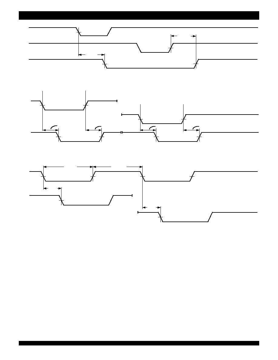
Figure 4. Full Flag From Last Write to First Read
Figure 2. Reset
Figure 3. Asynchronous Write and Read Operation
LAST WRITE
R
IGNORED
WRITE
FIRST READ
ADDITIONAL
READS
W
FF
t
WFF
t
RFF
3966 drw 06
FIRST
WRITE
t
A
R
t
RC
DATA OUT VALID
DATA OUT VALID
t
RPW
t
RLZ
t
DV
t
A
t
RHZ
t
RR
t
WC
t
WR
t
WPW
DATA IN VALID
DATA IN VALID
t
DS
t
DH
W
Q
0
-Q
8
D
0
-D
8
3966 drw 05
W
RS
R
EF
HF
,
FF
t
RSC
t
RS
t
RSS
t
RSS
t
RSR
t
EFL
t
HFH,
t
FFH
3966 drw 04
6
Commercial Temperature Range
IDT72V81/72V82/72V83/72V84/72V85
Figure 5. Empty Flag From Last Read to First Write
Figure 8. Minimum Timing for an Full Flag Coincident Write Pulse
Figure 7. Minimum Timing for an Empty Flag Coincident Read Pulse
Figure 6. Retransmit
FF
R
W
t
RFF
t
WPF
3966 drw 10
EF
W
R
t
WEF
t
RPE
3966 drw 09
t
RTC
t
RT
t
RTS
RT
W
,
R
HF
,
EF
,
FF
t
RTR
FLAG VALID
t
RTF
3966 drw 08
LAST READ
R
IGNORED
READ
FIRST WRITE
ADDITIONAL
WRITES
W
EF
t
WEF
VALID
t
A
DATA OUT
t
REF
3966 drw 07
FIRST READ
VALID
7
Commercial Temperature Range
IDT72V81/72V82/72V83/72V84/72V85
Figure 9. Half-Full Flag Timing
Figure 10. Expansion Out
Figure 11. Expansion In
OPERATING MODES:
Care must be taken to assure that the appropriate flag is monitored by each
system (i.e.
FF is monitored on the device where W is used; EF is monitored on
the device where
R is used).
Single Device Mode
A single IDT72V81/72V82/72V83/72V84/72V85 may be used when the
application requirements are for 512/1,024/2,048/4,096/8,192 words or less.
These FIFOs are in a Single Device Configuration when the Expansion In (
XI)
control input is grounded (see Figure 12).
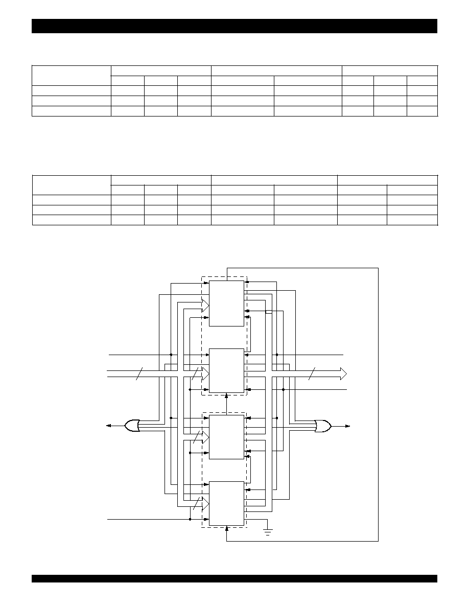
Depth Expansion
These devices can easily be adapted to applications when the requirements
are for greater than 512/1,024/2,048/4,096/8,192 words. Figure 14 demon-
strates a four-FIFO Depth Expansion using two IDT72V81/72V82/72V83/
72V84/72V85s. Any depth can be attained by adding additional IDT72V81/
72V82/72V83/72V84/72V85s. These FIFOs operate in the Depth Expansion
mode when the following conditions are met:
1. The first FIFO must be designated by grounding the First Load (
FL) control
input.
2. All other FIFOs must have
FL in the high state.
3. The Expansion Out (
XO) pin of each device must be tied to the Expansion
In (
XI) pin of the next device. See Figure 14.
4. External logic is needed to generate a composite Full Flag (
FF) and Empty
Flag (
EF). This requires the ORing of all EFs and ORing of all FFs (i.e. all
must be set to generate the correct composite
FF or EF). See Figure 14.
5. The Retransmit (
RT) function and Half-Full Flag (HF) are not available in
the Depth Expansion Mode.
W
XI
R
WRITE TO
FIRST PHYSICAL
LOCATION
READ FROM
FIRST PHYSICAL
LOCATION
t
XIS
t
XIR
t
XI
t
XIS
3966 drw 13
R
W
XO
3966 drw 12
WRITE TO
LAST PHYSICAL
LOCATION
t
XOL
t
XOH
READ FROM
LAST PHYSICAL
LOCATION
t
XOL
t
XOH
R
W
HF
t
RHF
3966 drw 11
HALF-FULL OR LESS
MORE THAN HALF-FULL
HALF-FULL OR LESS
t
WHF
8
Commercial Temperature Range
IDT72V81/72V82/72V83/72V84/72V85
USAGE MODES:
Width Expansion
Word width may be increased simply by connecting the corresponding
input control signals of multiple FIFOs. Status flags (
EF, FF and HF) can be
detected from any one FIFO. Figure 13 demonstrates an 18-bit word width by
using the two FIFOs contained in the IDT72V81/72V82/72V83/72V84/72V85s.
Any word width can be attained by adding FIFOs (Figure 13).
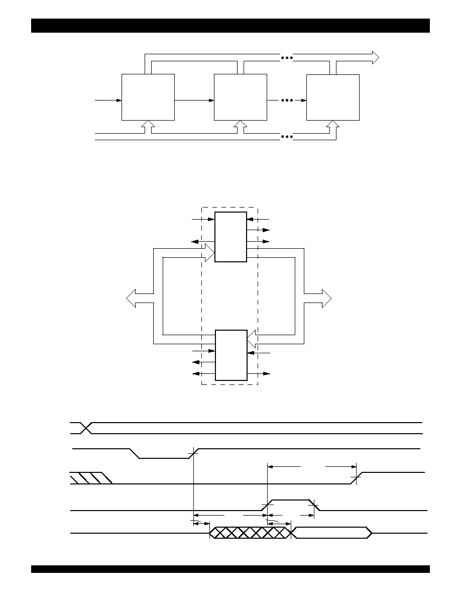
Bidirectional Operation
Applications which require data buffering between two systems (each
system capable of Read and Write operations) can be achieved by pairing
IDT72V81/72V82/72V83/72V84/72V85s as shown in Figure 16. Both Depth
Expansion and Width Expansion may be used in this mode.
Data Flow-Through
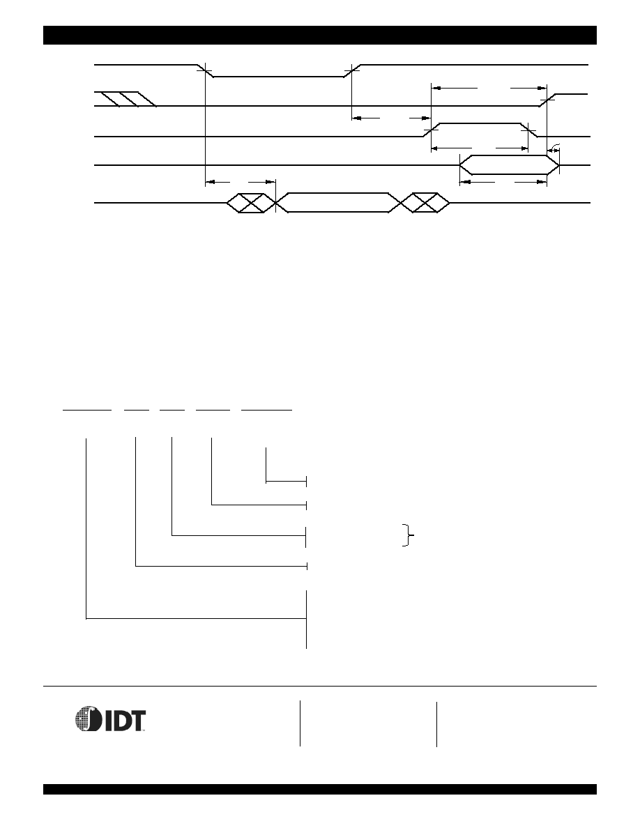
Two types of flow-through modes are permitted, a read flow-through
and write flow-through mode. For the read flow-through mode (Figure 17), the
FIFO permits a reading of a single word after writing one word of data into an
empty FIFO. The data is enabled on the bus in (t
WEF
+ t
A
) ns after the rising
edge of
W, called the first write edge, and it remains on the bus until the R line
is raised from low-to-high, after which the bus would go into a three-state mode
after t
RHZ
ns. The
EF line would have a pulse showing temporary deassertion
and then would be asserted.
In the write flow-through mode (Figure 18), the FIFO permits the writing
of a single word of data immediately after reading one word of data from a
full FIFO. The
R line causes the FF to be deasserted but the W line being low
causes it to be asserted again in anticipation of a new data word. On the rising
edge of
W, the new word is loaded in the FIFO. The W line must be toggled when
FF is not asserted to write new data in the FIFO and to increment the write pointer.
Compound Expansion
The two expansion techniques described above can be applied together
in a straightforward manner to achieve large FIFO arrays (see Figure 15).
Figure 12. Block Diagram of One 512 x 9, 1,024 x 9, 2,048 x 9, 4,096 x 9 and 8,192 x 9 FIFO Used in Single Device Mode
Figure 13. Block Diagram of One 512 x 18, 1,024 x 18, 2,048 x 18, 4,096 x 18 and 8,192 x 18 FIFO Memory Used in Width Expansion Mode
XIA
XIB
9
9
18
9
18
HFB
HFA
9
WRITE (
W
)
FULL FLAG (
FFA
)
RESET (
RS
)
READ (
R
)
EMPTY FLAG (
EFB
)
RETRANSMIT (
RT
)
DATA
OUT
(Q)
3966 drw 15
FIFO A
FIFO B
72V81/72V82/72V83
72V84/72V85
DATA
(D)
IN
WRITE (
W
)
DATA IN (D)
FULL FLAG (
FF
)
RESET (
RS
)
9
READ (
R
)
9
DATA OUT (Q)
EMPTY FLAG (
EF
)
RETRANSMIT (
RT
)
EXPANSION IN (
XI
)
(
HF
)
IDT
72V81
72V82
72V83
72V84
72V85
(HALF-FULL FLAG)
3966 drw 14
FIFO
A or B
9
Commercial Temperature Range
IDT72V81/72V82/72V83/72V84/72V85
TABLE IIRESET AND FIRST LOAD TRUTH TABLE
Depth Expansion/Compound Expansion Mode
Inputs
Internal Status
Outputs
Mode
RS
RS
RS
RS
RS
FL
FL
FL
FL
FL
XI
XI
XI
XI
XI
Read Pointer
Write Pointer
EF
EF
EF
EF
EF
FF
FF
FF
FF
FF
Reset First Device
0
0
(1)
Location Zero
Location Zero
0
1
Reset All Other Devices
0
1
(1)
Location Zero
Location Zero
0
1
Read/Write
1
X
(1)
X
X
X
X
NOTE:
1.
XI is connected to XO of previous device. See Figure 14. RS = Reset Input, FL/RT = First Load/Retransmit, EF = Empty Flag Output, FF = Full Flag Output,
XI = Expan-
sion Input,
HF = Half-Full Flag Output
TABLE IRESET AND RETRANSMIT
Single Device Configuration/Width Expansion Mode
Inputs
Internal Status
Outputs
Mode
RS
RS
RS
RS
RS
RT
RT
RT
RT
RT
XI
XI
XI
XI
XI
Read Pointer
Write Pointer
EF
EF
EF
EF
EF
FF
FF
FF
FF
FF
HF
HF
HF
HF
HF
Reset
0
X
0
Location Zero
Location Zero
0
1
1
Retransmit
1
0
0
Location Zero
Unchanged
X
X
X
Read/Write
1
1
0
Increment
(1)
Increment
(1)
X
X
X
NOTE:
1. Pointer will increment if flag is High.
Figure 14. Block Diagram of 2,048 x 9, 4,096 x 9, 8,192 x 9, 16,384 x 9 and 32,768 x 9 FIFO Memory (Depth Expansion)
D
W
FFB
EFB
FLB
XOB
RSA
FULL
EMPTY
V
CC
R
9
9
9
9
XIB
9
Q
FFA
EFA
FLA
XOA
XIA
FFB
EFB
FLB
XIB
3966 drw 16
XOA
FIFO A
FIFO B
FIFO A
FIFO B
XIA
XOB
EFA
FLA
FFA
72V81/72V82
72V83/72V84
72V85
72V81/72V82
72V83/72V84
72V85
10
Commercial Temperature Range
IDT72V81/72V82/72V83/72V84/72V85
NOTES:
1. For depth expansion block see section on Depth Expansion and Figure 14.
2. For Flag detection see section on Width Expansion and Figure 13.
Figure 15. Compound FIFO Expansion
Figure 17. Read Data Flow-Through Mode
Figure 16. Bidirectional FIFO Mode
W
DATA
R
t
RPE
IN
EF
DATA
OUT
t
WLZ
t
WEF
t
A
t
REF
DATA VALID
OUT
3966 drw 19
IDT
7201A
R
A
EF
A
HF
A
W
A
FF
A
W
B
FF
B
SIDE 1
SIDE 2
Q
A 0-8
D
A 0-8
Q
B 0-8
R
B
HF
B
EF
B
IDT
72V81
72V82
72V83
72V84
72V85
D
A 0-8
FIFO B
3966 drw 18
FIFO A
IDT
72V81/72V82/72V83
72V84/72V85
DEPTH
EXPANSION
BLOCK
R
,
W
,
RS
D
0
-D
N
Q
0
-Q
8
Q
(N-8)
-Q
N
3966 drw 17
Q
9
-Q
17
Q
0
-Q
8
Q
9
-Q
17
Q
(N-8)
-Q
N
D
(N-8)
-D
N
D
9
-D
17
D
9
-D
N
D
18
-D
N
D
(N-8)
-D
N
D
0
-D
8
IDT
72V81/72V82/72V83
72V84/72V85
DEPTH
EXPANSION
BLOCK
IDT
72V81/72V82/72V83
72V84/72V85
DEPTH
EXPANSION
BLOCK
11
*To search for sales office near you, please click the sales button found on our home page or dial the 800# above and press 2.
The Async FIFO is a trademark and the IDT logo is a registered trademark of Integrated Device Technology, Inc.
CORPORATE HEADQUARTERS
for SALES:
for Tech Support:
2975 Stender Way
800-345-7015 or 408-727-6116
408-330-1753
Santa Clara, CA 95054
fax: 408-492-8674
email: FIFOhelp@idt.com
www.idt.com*
PFPkg: www.idt.com/docs/PSC4039.pdf
IDT
XXXX
Device Type
XXX
Speed
X
Power
X
Package
X
Process/
Temperature
Range
Blank
72V81
72V82
72V83
72V84
72V85
15
20
L
PA
Commercial (0
∞
C to +70
∞
C)
512 x 9
3.3V Dual FIFO
1,024 x 9
3.3V Dual FIFO
2,048 x 9
3.3V Dual FIFO
4,096 x 9
3.3V Dual FIFO
8,192 x 9
3.3V Dual FIFO
Low Power
Thin Shrink SOIC (TSSOP, S056-2)
Access Time (t
A
) Speed
in Nanoseconds
3966 drw 21
Commercial
Figure 18. Write Data Flow-Through Mode
ORDERING INFORMATION
NOTE:
1. Industrial temperature range is available by special order.
R
DATA
W
IN
FF
DATA
OUT
t
DS
t
DH
t
A
t
WFF
t
RFF
t
WPF
DATA
IN
VALID
DATA
OUT
VALID
3966 drw 20