 | –≠–ª–µ–∫—Ç—Ä–æ–Ω–Ω—ã–π –∫–æ–º–ø–æ–Ω–µ–Ω—Ç: 72V90823 | –°–∫–∞—á–∞—Ç—å:  PDF PDF  ZIP ZIP |
1
2002 Integrated Device Technology, Inc. All rights reserves. Product specifications subject to change without notice.
DSC-5712/4
DECEMBER 2002
3.3 VOLT TIME SLOT INTERCHANGE
DIGITAL SWITCH
2,048 x 2,048
IDT72V90823
IDT and the IDT logo are registered trademarks of Integrated Device Technology, Inc. The ST-BUS is a trademark of Mitel Corp.
FUNCTIONAL BLOCK DIAGRAM
RX0
RX1
RX2
RX3
RX4
RX5
RX6
RX7
ODE
F0i
V
CC
CS
DS/
RD
R/
W/
WR
A0-A7
GND
CCO
DTA D8-D15/
AD0-AD7
RX8
RX9
RX10
RX11
RX12
RX13
RX14
RX15
TX0
TX1
TX2
TX3
TX4
TX5
TX6
TX7
TX8
TX9
TX10
TX11
TX12
TX13
TX14
TX15
AS/
ALE
IM
CLK
FE/
HCLK
WFPS
TDI
TMS
TCK
TDO
TRST
RESET
IC
5712 drw01
Receive
Serial Data
Streams
Output
MUX
Loopback
Test Port
Data Memory
Internal
Registers
Microprocessor Interface
Timing Unit
Connection
Memory
Transmit
Serial Data
Streams
FEATURES:
∑
2,048 x 2,048 channel non-blocking switching at 8.192 Mb/s
∑
Per-channel variable or constant throughput delay
∑
Automatic identification of ST-BUS
Æ
/GCI interfaces
∑
Accept streams of 2.048 Mb/s, 4.096 Mb/s or 8.192 Mb/s
∑
Automatic frame offset delay measurement
∑
Per-stream frame delay offset programming
∑
Per-channel high impedance output control
∑
Per-channel Processor Mode
∑
Control interface compatible to Intel/Motorola CPUs
∑
Connection memory block programming
∑
IEEE-1149.1 (JTAG) Test Port
∑
Available in 84-pin Plastic Leaded Chip Carrier (PLCC),
100-pin Ball Grid Array (BGA), 100-pin Plastic Quad Flatpack
(PQFP) and 100-pin Thin Quad Flatpack (TQFP)
∑
3.3V Power Supply
∑
Operating Temperature Range -40
∞∞
∞∞
∞C to +85∞∞∞∞∞C
DESCRIPTION:
The IDT72V90823 is a non-blocking digital switch that has a capacity of
2,048 x 2,048 channels at a serial bit rate of 8.192 Mb/s, 1,024 x 1,024 channels
at 4.096 Mb/s and 512 x 512 channels at 2.048 Mb/s. Some of the main features
are: programmable stream and channel control, Processor Mode, input offset
delay and high-impedance output control.
Per-stream input delay control is provided for managing large multi-chip
switches that transport both voice channel and concatenated data channels. In
addition, input streams can be individually calibrated for input frame offset.
2
COMMERCIAL TEMPERATURE RANGE
IDT72V90823 3.3V TIME SLOT INTERCHANGE
DIGITAL SWITCH 2,048 x 2,048
PIN CONFIGURATIONS
12
13
14
15
16
17
18
19
20
4
3
2
1
83 82 81
39 40 41 42 43 44 45
INDEX
5712 drw03
7
6
5
80 79 78 77 76 75
8
11 10 9
46 47 48 49 50 51 52
33 34 35 36 37 38
64
63
62
61
60
59
58
57
56
73
72
71
70
69
68
67
66
65
55
54
21
22
23
24
25
26
27
28
29
30
31
32
53
74
84
CCO
DTA
D15
D14
D13
D12
D11
D10
D9
D8
GND
VCC
AD7
AD6
AD5
AD4
AD3
AD2
AD1
AD0
GND
RX0
RX1
RX2
RX3
RX4
RX5
RX6
RX7
RX8
RX9
RX10
RX11
RX12
RX13
RX14
RX15
F0i
FE/HCLK
GND
CLK
VCC
TMS
TDI
TDO
TCK
TRST
IC
RESET
WFPS
A0
A1
A2
A3
A4
A5
A6
A7
DS/
RD
R/
W
/
RW
CS
AS/ALE
IM
GND
TX15
TX14
TX13
TX12
TX11
TX10
TX9
TX8
VCC
GND
TX7
TX6
TX5
TX4
TX3
TX2
TX1
TX0
ODE
GND
A
B
C
D
E
F
G
H
J
K
RX0
RX2
RX7
RX10
RX5
RX11
RX13
RX14
FOI
TMS
TX13
RX1
RX8
RX9
RX4
RX12
RX15
FE/
HCLK
TDI
TDO
TX11
TX14
RX6
VCC
RX3
VCC
CLK
TCK
TRST
IC
TX10
TX12
VCC
D11
D14
CCO
D13
ODE
TX0
D10
DTA
TX2
TX3
VCC
VCC
TX5
TX4
GND
GND
GND
GND
GND
TX6
TX7
GND
TX9
TX8
10
9
8
7
6
5
4
3
2
1
A1 BALL PAD CORNER
D9
D12
D8
AD5
AD3
AD0
AS/ALE
DNC
GND
VCC
CS
A7
A5
VCC
GND
GND
VCC
A4
A3
A6
D15
AD7
AD6
AD2
IM
DS/RD
TX1
VCC
AD4
AD1
R/
W/RW
VCC
GND
GND
VCC
A1
A2
TX15
GND
VCC
RESET
A0
WFPS
5712 drw02
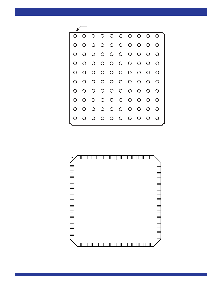
BGA: 1mm pitch, 11mm x 11mm (BC100-1, order code: BC)
TOP VIEW
PLCC: 0.05in. pitch, 1.15in. x 1.15in. (PL84-1, order code: J)
TOP VIEW
NOTES:
1. DNC - Do Not Connect
2. IC - Internal Connection, tie to GROUND for normal operation.
3. All I/O pins are 5V tolerant except for TMS, TDI and
TRST.
3
COMMERCIAL TEMPERATURE RANGE
IDT72V90823 3.3V TIME SLOT INTERCHANGE
DIGITAL SWITCH 2,048 x 2,048
INDEX
5712 drw04
1
2
3
4
5
6
7
8
9
10
11
12
13
14
15
16
17
18
19
20
21
22
23
24
25
76
77
78
79
80
81
82
83
84
85
86
87
88
89
90
91
92
93
94
95
96
97
98
99
100
50
49
48
47
46
45
44
43
42
41
40
39
38
37
36
35
34
33
32
31
30
29
28
27
26
75
74
73
72
71
70
69
68
67
66
65
64
63
62
61
60
59
58
57
56
55
54
53
52
51
DNC
DNC
RX0
RX1
RX2
RX3
RX4
RX5
RX6
RX7
RX8
RX9
RX10
RX11
RX12
RX13
RX14
RX15
F0i
FE/HCLK
GND
CLK
VCC
CCO
DTA
D15
D14
D13
D12
D11
D10
D9
D8
GND
VCC
AD7
AD6
AD5
AD4
AD3
AD2
AD1
AD0
GND
DNC
DNC
DNC
DNC
TMS
TDI
TDO
TCK
TRST
IC
RESET
WFPS
A0
A1
A2
A3
A4
A5
A6
A7
DS/
RD
R/
W
/
RW
CS
AS/ALE
IM
GND
TX15
TX14
TX13
TX12
TX11
TX10
TX9
TX8
VCC
GND
TX7
TX6
TX5
TX4
TX3
TX2
TX1
TX0
ODE
GND
DNC
DNC
DNC
DNC
DNC
DNC
DNC
DNC
DNC
DNC
PIN CONFIGURATIONS (CONTINUED)
INDEX
5712 drw05
1
2
3
4
5
6
7
8
9
10
11
12
13
14
15
16
17
18
19
20
21
22
23
24
25
26
27
28
29
30
50
49
48
47
46
45
44
43
42
41
40
39
38
37
36
35
34
33
32
31
80
79
78
77
76
75
74
73
72
71
70
69
68
67
66
65
64
63
62
61
60
59
58
57
56
55
54
53
52
51
RX0
RX1
RX2
RX3
RX4
RX5
RX6
RX7
RX8
RX9
RX10
RX11
RX12
RX13
RX14
RX15
FOi
FE/HCLK
CLK
DTA
D15
D14
D13
D12
D11
D10
D9
D8
GND
VCC
AD7
AD6
AD5
AD4
AD3
AD2
AD1
AD0
GND
DNC
DNC
DNC
DNC
VCC
TMS
TDI
TDO
TCK
TRST
IC
RESET
WFPS
A0
A1
A2
A3
A4
A5
A6
A7
DS/
RD
R/
W
/
WR
CS
AS/ALE
IM
DNC
DNC
DNC
DNC
DNC
DNC
DNC
DNC
GND
TX15
TX14
TX13
TX12
TX11
TX10
TX9
TX8
VCC
GND
TX7
TX6
TX5
TX4
TX3
TX2
TX1
TX0
ODE
GND
CCO
DNC
DNC
DNC
DNC
GND
81
82
83
84
85
86
87
88
89
90
91
92
93
94
95
96
97
98
100
99
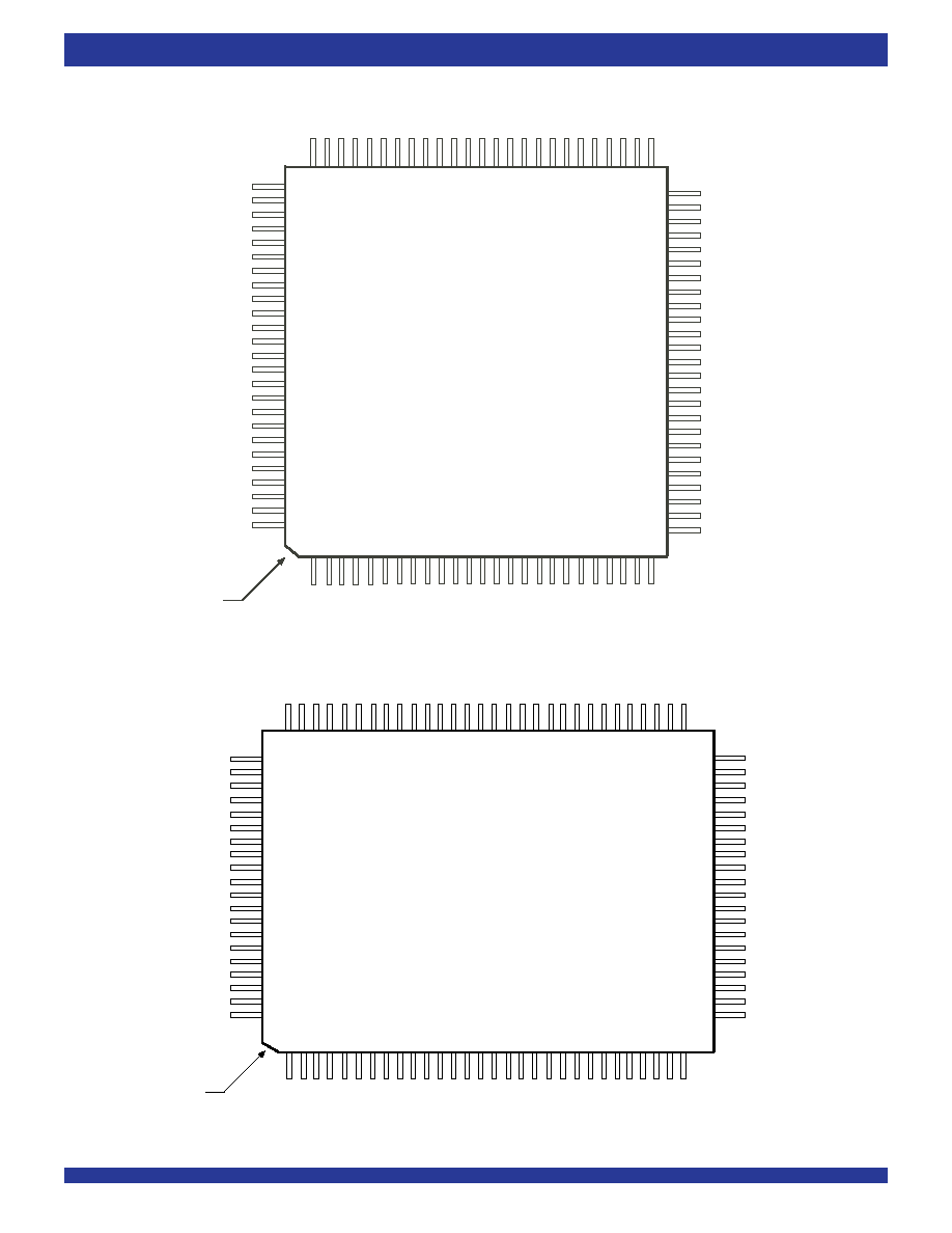
PQFP: 0.65mm pitch, 14mm x 20mm (PQ100-2, order code: PQF)
TOP VIEW
TQFP: 0.50mm pitch, 14mm x 14mm (PN100-1, order code: PF)
TOP VIEW

4
COMMERCIAL TEMPERATURE RANGE
IDT72V90823 3.3V TIME SLOT INTERCHANGE
DIGITAL SWITCH 2,048 x 2,048
PIN DESCRIPTION
SYMBOL
NAME
I/O
DESCRIPTION
GND
Ground.
Ground Rail.
Vcc
Vcc
+3.3 Volt Power Supply.
TX0-15
(1)
TX Output 0 to 15
O
Serial data output stream. These streams may have data rates of 2.048, 4.096 or 8.192 Mb/s, depending upon
(Three-state Outputs)
the value programmed at bits DR0-1 in the IMS register.
RX0-15
(1)
RX Input 0 to 15
I
Serial data input stream. These streams may have data rates of 2.048, 4.096 or 8.192 Mb/s, depending upon
the value programmed at bits DR0-1 in the IMS register.
F0i
(1)
Frame Pulse
I
When the WFPS pin is LOW, this input accepts and automatically identifies frame synchronization signals formatted
according to ST-BUS
Æ
and GCI specifications. When the WFPS pin is HIGH, this pin accepts a negative frame
pulse which conforms to WFPS formats.
FE/HCLK
(1)
Frame Evaluation/
I
When the WFPS pin is LOW, this pin is the frame measurement input. When the WFPS pin is HIGH, the HCLK
HCLK Clock
(4.096 MHz clock) is required for frame alignment in the wide frame pulse (WFP) mode.
CLK
(1)
Clock
I
Serial clock for shifting data in/out on the serial streams (RX/TX 0-15). Depending upon the value programmed
at bits DR0-1 in the IMS register, this input accepts a 4.096, 8.192 or 16.384 MHz clock.
TMS
Test Mode Select
I
JTAG signal that controls the state transitions of the TAP controller. This pin is pulled HIGH by an internal pull-
up when not driven.
TDI
Test Serial Data In
I
JTAG serial test instructions and data are shifted in on this pin. This pin is pulled HIGH by an internal pull-up
when not driven.
TDO
Test Serial Data Out
O
JTAG serial data is output on this pin on the falling edge of TCK. This pin is held in high-impedance state when
JTAG scan is not enabled.
TCK
(1)
Test Clock
I
Provides the clock to the JTAG test logic.
TRST
Test Reset
I
Asynchronously initializes the JTAG TAP controller by putting it in the Test-Logic-reset state. This pin is pulled
by an internal pull-up when not driven. This pin should be pulsed LOW on power-up, or held LOW, to ensure
that the IDT72V90823 is in the normal functional mode.
IC
(1)
Internal Connection
I
Connect to GND for normal operation. This pin must be low for the IDT72V90823 to function normally and to comply
with IEEE 1114 (JTAG) boundary scan requirements.
RESET
(1)
Device Reset
I
This input (active LOW) puts the IDT72V90823 in its reset state that clears the device internal counters, registers
(Schmitt Trigger Input)
and brings TX0-15 and microport data outputs to a high-impedance state. The time constant for a power up
reset circuit must be a minimum of five times the rise time of the power supply. In normal operation, the
RESET
pin must be held LOW for a minimum of 100ns to reset the device.
WFPS
(1)
Wide Frame
I
When 1, enables the wide frame pulse (WFP) Frame Alignment interface. When 0, the device operates in
Pulse Select
ST-BUS
Æ
/GCI mode.
A0-7
(1)
Address 0-7
I
When non-multiplexed CPU bus operation is selected, these lines provide the A0-A7 address lines to the internal
memories.
DS/
RD
(1)
Data Strobe/Read
I
For Motorola multiplexed bus operation, this input is DS. This active HIGH DS input works in conjunction with
CS
to enable the read and write operations. For Motorola non-multiplexed CPU bus operation, this input is DS. This
active LOW input works in conjunction with
CS to enable the read and write operations. For Intel multiplexed bus
operation, this input is
RD. This active LOW input sets the data bus lines (AD0-7, D8-15) as outputs.
R/
W / WR
(1)
Read/Write / Write
I
In the cases of Motorola non-multiplexed and multiplexed bus operations, this input is R/
W. This input controls
the direction of the data bus lines (AD0-7, D8-15) during a microprocessor access. For Intel multiplexed bus
operation, this input is
WR. This active LOW input is used with RD to control the data bus (AD0-7) lines as inputs.
CS
(1)
Chip Select
I
Active LOW input used by a microprocessor to activate the microprocessor port of IDT72V90823.
AS/ALE
(1)
Address Strobe or
I
This input is used if multiplexed bus operation is selected via the IM input pin. For Motorola non-multiplexed
Latch Enable
bus operation, connect this pin to ground.
NOTE:
1. These pins are 5V tolerant.

5
COMMERCIAL TEMPERATURE RANGE
IDT72V90823 3.3V TIME SLOT INTERCHANGE
DIGITAL SWITCH 2,048 x 2,048
IM
(1)
CPU Interface Mode
I
When IM is HIGH, the microprocessor port is in the multiplexed mode. When IM is LOW, the microprocessor
port is in non-multiplexed mode.
AD0-7
(1)
Address/Data Bus
I/O
These pins are the eight least significant data bits of the microprocessor port. In multiplexed mode, these pins
0 to 7
are also the input address bits of the microprocessor port.
D8-15
(1)
Data Bus 8-15
I/O
These pins are the eight most significant data bits of the microprocessor port.
DTA
(1)
Data Transfer
O
This active LOW output signal indicates that a data bus transfer is complete. When the bus cycle ends, this pin
Acknowledgment
drives HIGH and then goes high-impedance, allowing for faster bus cycles with a weaker pull-up resistor. A
pull-up resistor is required to hold a HIGH level when the pin is in high-impedance.
CCO
(1)
Control Output
O
This is a 4.096, 8.192 or 16.384 Mb/s output containing 512, 1,024 or 2.048 bits per frame respectively. The
level of each bit is determined by the CCO bit in the connection memory. See External Drive Control Section.
ODE
(1)
Output Drive Enable
I
This is the output enable control for the TX0 to TX15 serial outputs. When ODE input is LOW and the OSB
bit of the IMS register is LOW, TX0-15 are in a high-impedance state. If this input is HIGH, the TX0-15
output drivers are enabled. However, each channel may still be put into a high-impedance state by using the
per channel control bit in the connection memory.
PIN DESCRIPTION (CONTINUED)
SYMBOL
NAME
I/O
DESCRIPTION
NOTE:
1. These pins are 5V tolerant.

6
COMMERCIAL TEMPERATURE RANGE
IDT72V90823 3.3V TIME SLOT INTERCHANGE
DIGITAL SWITCH 2,048 x 2,048
FUNCTIONAL DESCRIPTION
The IDT72V90823 is capable of switching up to 2,048 x 2,048, 64 Kbit/s
PCM or N x 64 Kbit/s channel data. The device maintains frame integrity in data
applications and minimum throughput delay for voice applications on a per
channel basis.
The serial input streams of the IDT72V90823 can have a bit rate of 2.048,
4.096 or 8.192 Mb/s and are arranged in 125
µs wide frames, which contain
32, 64 or 128 channels respectively. The data rates on input and output streams
are identical.
In Processor Mode, the microprocessor can access input and output time-
slots on a per channel basis allowing for transfer of control and status information.
The IDT72V90823 automatically identifies the polarity of the frame synchroni-
zation input signal and configures the serial streams to either ST-BUS
Æ
or GCI
formats.
With the variety of different microprocessor interfaces, IDT72V90823 has
provided an Input Mode pin (IM) to help integrate the device into different
microprocessor based environments: Non-multiplexed or Multiplexed. These
interfaces provide compatibility with multiplexed and Motorola non-multiplexed
buses. The device can also resolve different control signals eliminating the use
of glue logic necessary to convert the signals (R/
W/WR, DS/RD, AS/ALE).
The frame offset calibration function allows users to measure the frame offset
delay using a frame evaluation pin (FE). The input offset delay can be
programmed for individual streams using internal frame input offset registers, see
Table 11.
The internal loopback allows the TX output data to be looped around to the
RX inputs for diagnostic purposes.
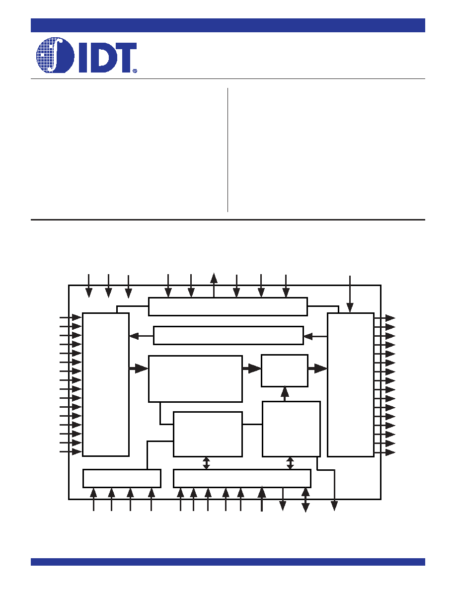
A functional Block Diagram of the IDT72V90823 is shown in Figure 1.
DATA AND CONNECTION MEMORY
The received serial data is converted to parallel format by internal serial-
to-parallel converters and stored sequentially in the data memory. The 8 KHz
input frame pulse (
F0i) is used to generate channel and frame boundaries of
the input serial data. Depending on the interface mode select (IMS) register,
the usable data memory may be as large as 2,048 bytes.
Data to be output on the serial streams (TX0-15) may come from either the
data memory or connection memory. For data output from data memory
(connection mode), addresses in the connection memory are used. For data
to be output from connection memory, the connection memory control bits must
set the particular TX output in Processor Mode. One time-slot before the data
is to be output, data from either connection memory or data memory is read
internally. This allows enough time for memory access and parallel-to-serial
conversion.
CONNECTION AND PROCESSOR MODES
In the Connection Mode, the addresses of the input source data for all output
channels are stored in the connection memory. The connection memory is
mapped in such a way that each location corresponds to an output channel on
the output streams. For details on the use of the source address data (CAB and
SAB bits), see Table 13 and Table 14. Once the source address bits are
programmed by the microprocessor, the contents of the data memory at the
selected address are transferred to the parallel-to-serial converters and then
onto a TX output stream.
By having the each location in the connection memory specify an input
channel, multiple outputs can specify the same input address. This can be a
powerful tool used for broadcasting data.
In Processor Mode, the microprocessor writes data to the connection
memory. Each location in the connection memory corresponds to a particular
output stream and channel number and is transferred directly to the parallel-to-
serial converter one time-slot before it is to be output. This data will be output
on the TX streams in every frame until the data is changed by the microprocessor.
As the IDT72V90823 can be used in a wide variety of applications, the device
also has memory locations to control the outputs based on operating mode.
Specifically, the IDT72V90823 provides five per-channel control bits for the
following functions: processor or connection mode, constant or variable delay,
enables/three-state the TX output drivers and enables/disable the loopback
function. In addition, one of these bits allows the user to control the CCO output.
If an output channel is set to a high-impedance state through the connection
memory, the TX output will be in a high-impedance state for the duration of that
channel. In addition to the per-channel control, all channels on the ST-BUS
Æ
outputs can be placed in a high impedance state by either pulling the ODE input
pin low or programming the Output Stand-By (OSB) bit in the interface mode
selection register. This action overrides the per-channel programming in the
connection memory bits.
The connection memory data can be accessed via the microprocessor
interface. The addressing of the devices internal registers, data and connection
memories is performed through the address input pins and the Memory Select
(MS) bit of the control register. For details on device addressing, see Software
Control and Control Register bits description (Table 4, 6 and 7).
SERIAL DATA INTERFACE TIMING
The master clock frequency must always be twice the data rate. For serial
data rates of 2.048, 4.096 or 8.192 Mb/s, the master clock (CLK) must be either
at 4.096, 8.192 or 16.384 MHz respectively. The input and output stream data
rates will always be identical.
The IDT72V90823 provides two different interface timing modes ST-BUS
Æ
/
GCI and WFP (wide frame pulse). If the WFPS pin is high, the IDT72V90823
is in the wide frame pulse (WFP) frame alignment mode.
In ST-BUS
Æ
/GCI mode, the input 8 KHz frame pulse can be in either
ST-BUS
Æ
or GCI format. The IDT72V90823 automatically detects the presence
of an input frame pulse and identifies it as either ST-BUS
Æ
or GCI. In ST-BUS
Æ
format, every second falling edge of the master clock marks a bit boundary and
the data is clocked in on the rising edge of CLK, three quarters of the way into
the bit cell, see Figure 7. In GCI format, every second rising edge of the master
clock marks the bit boundary and data is clocked in on the falling edge of CLK
at three quarters of the way into the bit cell, see Figure 8.
WIDE FRAME PULSE (WFP) FRAME ALIGNMENT TIMING
When the device is in WFP frame alignment mode, the CLK input must be
at 16.384 MHz, the FE/HCLK input is 4.096 MHz and the 8 kHz frame pulse
is in ST-BUS
Æ
format. The timing relationship between CLK, HCLK and the frame
pulse is shown in Figure 9.
When WFPS pin is high, the frame alignment evaluation feature is disabled.
However, the frame input offset registers may still be programmed to compensate
for the varying frame delays on the serial input streams.

7
COMMERCIAL TEMPERATURE RANGE
IDT72V90823 3.3V TIME SLOT INTERCHANGE
DIGITAL SWITCH 2,048 x 2,048
TABLE 1
-- SWITCHING CONFIGURATION
SWITCHING CONFIGURATIONS
The IDT72V90823 can operate at different speeds. To configure the
maximum non-blocking switching data rate, the two DR bits in the IMS register
are used. Following are the possible configurations:
2.048 Mb/s Serial Links (DR0=0, DR1=0)
When the 2.048 Mb/s data rate is selected, the device is configured with
16-input/16-output data streams each having 32, 64 Kbit/s channels each. This
mode requires a CLK of 4.096 MHz and allows a maximum non-blocking
capacity of 512 x 512 channels.
4.096 Mb/s Serial Links (DR0=1, DR1=0)
When the 4.096 Mb/s data rate is selected, the device is configured with
16-input/16-output data streams each having 64, 64 Kbit/s channels each. This
mode requires a CLK of 8.192 MHz and allows a maximum non-blocking
capacity of 1,024 x 1,024 channels.
8.192 Mb/s Serial Links (DR0=0, DR1=1)
When the 8.192 Mb/s data rate is selected, the device is configured with
16-input/16-output data streams each having 128, 64 Kbit/s channels each. This
mode requires a CLK of 16.384 MHz and allows a maximum non-blocking
capacity of 2,048 x 2,048 channels.
Table 1 summarizes the switching configurations and the relationship
between different serial data rates and the master clock frequencies.
INPUT FRAME OFFSET SELECTION
Input frame offset selection allows the channel alignment of individual input
streams to be offset with respect to the output stream channel alignment (i.e.
F0i).
Although all input data comes in at the same speed, delays can be caused by
variable path serial backplanes and variable path lengths which may be
implemented in large centralized and distributed switching systems. Because
data is often delayed, this feature is useful in compensating for the skew between
clocks.
Each input stream can have its own delay offset value by programming the
frame input offset registers (FOR). The maximum allowable skew is +4.5 master
clock (CLK) periods forward with resolution of 1/2 clock period. The output frame
offset cannot be offset or adjusted. See Figure 5, Table 11 and 12 for delay offset
programming.
SERIAL INPUT FRAME ALIGNMENT EVALUATION
The IDT72V90823 provides the frame evaluation (FE) input to determine
different data input delays with respect to the frame pulse
F0i.
A measurement cycle is started by setting the start frame evaluation (SFE)
bit low for at least one frame. When the SFE bit in the IMS register is changed
from low to high, the evaluation starts. Two frames later, the complete frame
evaluation (CFE) bit of the frame alignment register (FAR) changes from low
to high to signal that a valid offset measurement is ready to be read from bits 0
to 11 of the FAR register. The SFE bit must be set to zero before a new
measurement cycle started.
In ST-BUS
Æ
mode, the falling edge of the frame measurement signal (FE)
is evaluated against the falling edge of the ST-BUS
Æ
frame pulse. In GCI mode,
the rising edge of FE is evaluated against the rising edge of the GCI frame pulse.
See Table 10 & Figure 4 for the description of the frame alignment register.
This feature is not available when the WFP Frame Alignment mode is
enabled (i.e., when the WFPS pin is connected to VCC).
MEMORY BLOCK PROGRAMMING
The IDT72V90823 provides users with the capability of initializing the entire
connection memory block in two frames. To set bits 11 to 15 of every connection
memory location, first program the desired pattern in bits 5 to 9 of the IMS register.
The block programming mode is enabled by setting the memory block
program (MBP) bit of the control register high. When the block programming
enable (BPE) bit of the IMS register is set to high, the block programming data
will be loaded into the bits 11 to 15 of every connection memory location. The
other connection memory bits (bit 0 to bit 10) are loaded with zeros. When the
memory block programming is complete, the device resets the BPE bit to zero.
LOOPBACK CONTROL
The loopback control (LPBK) bit of each connection memory location allows
the TX output data to be looped backed internally to the RX input for diagnostic
purposes.
If the LPBK bit is high, the associated TX output channel data is internally
looped back to the RX input channel (i.e., data from TX n channel m routes to
the RX n channel m internally); if the LPBK bit is low, the loopback feature is
disabled. For proper per-channel loopback operation, the contents of frame
delay offset registers must be set to zero.
DELAY THROUGH THE IDT72V90823
The switching of information from the input serial streams to the output serial
streams results in a throughput delay. The device can be programmed to
perform time-slot interchange functions with different throughput delay capabili-
ties on the per-channel basis. For voice applications, variable throughput delay
is best as it ensures minimum delay between input and output data. In wideband
data applications, constant throughput delay is best as the frame integrity of the
information is maintained through the switch.
The delay through the device varies according to the type of throughput
delay selected in the
V/C bit of the connection memory.
VARIABLE DELAY MODE (
V/C BIT = 0)
In this mode, the delay is dependent only on the combination of source and
destination channels and is independent of input and output streams. The
minimum delay achievable in the IDT72V90823 is three time-slots. If the input
channel data is switched to the same output channel (channel n, frame p), it will
be output in the following frame (channel n, frame p+1). The same is true if input
channel n is switched to output channel n+1 or n+2. If the input channel n is
switched to output channel n+3, n+4,..., the new output data will appear in the
same frame. Table 2 shows the possible delays for the IDT72V90823 in the
variable delay mode.
Serial Interface
Master Clock Required
Matrix Channel
Data Rate
(MHz)
Capacity
2.048 Mb/s
4.096
512 x 512
4.096 Mb/s
8.192
1,024 x 1,024
8.192 Mb/s
16.384
2,048 x 2,048

8
COMMERCIAL TEMPERATURE RANGE
IDT72V90823 3.3V TIME SLOT INTERCHANGE
DIGITAL SWITCH 2,048 x 2,048
CONSTANT DELAY MODE (
V/C BIT = 1)
In this mode, frame integrity is maintained in all switching configurations by
making use of a multiple data memory buffer. Input channel data is written into
the data memory buffers during frame n will be read out during frame n+2. In
the IDT72V90823, the minimum throughput delay achievable in the constant
delay mode will be one frame. For example, in 2 Mb/s mode, when input time-
slot 31 is switched to output time-slot 0. The maximum delay of 94 time-slots of
delay occurs when time-slot 0 in a frame is switched to time-slot 31 in the frame.
See Table 3.
MICROPROCESSOR INTERFACE
The IDT72V90823 provides a parallel microprocessor interface for multi-
plexed or non-multiplexed bus structures. This interface is compatible with
Motorola non-multiplexed and multiplexed buses.
If the IM pin is low a Motorola non-multiplexed bus should be connected to
the device. If the IM pin is high, the device monitors the AS/ALE and DS/
RD to
determine what mode the IDT72V90823 should operate in.
If DS/
RD is low at the rising edge of AS/ALE, then the mode 1 multiplexed
timing is selected. If DS/
RD is high at the rising edge of AS/ALE, then the mode
2 multiplexed bus timing is selected.
For multiplexed operation, the required signals are the 8-bit data and
address (AD0-AD7), 8-bit Data (D8-D15), Address strobe/Address latch
enable (AS/ ALE), Data strobe/Read (DS/
RD), Read/Write /Write (R/W / WR),
Chip select (
CS) and Data transfer acknowledge (DTA). See Figure 12 and
Figure 13 for multiplexed parallel microport timing.
For the Motorola non-multiplexed bus, the required signals are the 16-bit
data bus (AD0-AD7, D8-D15), 8-bit address bus (A0-A7) and 4 control lines
(
CS, DS, R/W and DTA). See Figure 14 and 15 for Motorola non-multiplexed
microport timing.
The IDT72V90823 microport provides access to the internal registers,
connection and data memories. All locations provide read/write access except
for the data memory and the frame alignment register which are read only.
MEMORY MAPPING
The address bus on the microprocessor interface selects the internal
registers and memories of the IDT72V90823.
If the A7 address input is low, then A6 through A0 are used to address the
interface mode selection (IMS), control (CR), frame alignment (FAR) and frame
input offset (FOR) registers (Table 4). If the A7 is high, then A6 through A0 are
used to select 32, 64, or 128 locations corresponding to data rate of the ST-
BUS
Æ
. The address input lines and the stream address bits (STA) of the control
register allow access to the entire data and connection memories. The control
and IMS registers together control all the major functions of the device, see
Figure 3.
As explained in the Serial Data Interface Timing and Switching Configura-
tions sections, after system power-up, the IMS register should be programmed
immediately to establish the desired switching configuration.
The data in the control register consists of the memory block programming
bit (MBP), the memory select bit (MS) and the stream address bits (STA). As
explained in the Memory Block Programming section, the MBP bit allows the
entire connection memory block to be programmed. The memory select bit is
used to designate the connection memory or the data Memory. The stream
address bits select internal memory subsections corresponding to input or output
serial streams.
The data in the IMS register consists of block programming bits (BPD0-
BPD4), block programming enable bit (BPE), output stand by bit (OSB), start
frame evaluation bit (SFE) and data rate selection bits (DR0-1). The block
programming and the block programming enable bits allows users to program
the entire connection memory (see Memory Block Programming section). If the
ODE pin is low, the OSB bit enables (if high) or disables (if low) all ST-BUS
Æ
output drivers. If the ODE pin is high, the contents of the OSB bit is ignored and
all TX output drivers are enabled.
CONNECTION MEMORY CONTROL
The CCO pin is a 4.096, 8.192 or 16.384 Mb/s output, which carries 512,
1,024 or 2,048 bits, respectively. The contents of the CCO bit of each connection
memory location are output on the CCO pin once every frame. The contents
of the CCO bits of the connection memory are transmitted sequentially on to the
CCO pin and are synchronous with the data rates on the other serial streams.
The CCO bit is output one channel before the corresponding channel on
the serial streams. For example, in 2.048 Mb/s mode (32 channels per frame),
the contents of the CCO bit in position 0 (TX0, CH0) of the connection memory
is output on the first clock cycle of channel 31 through CCO pin. The contents
of the CCO bit in position 32 (TX1, CH0) of the connection memory is output on
the second clock cycle of channel 31 via CCO pin.
If the ODE pin or the OSB bit is high, the OE bit of each connection memory
location controls the output drivers-enables (if high) or disables (if low). See
Table 5 for detail.
The processor channel (PC) bit of the connection memory selects between
Processor Mode and Connection Mode. If high, the contents of the connection
memory are output on the TX streams. If low, the stream address bit (SAB) and
the channel address bit (CAB) of the connection memory defines the source
information (stream and channel) of the time-slot that will be switched to the output
from data memory.
The
V/C (Variable/Constant Delay) bit in each connection memory location
allows the per-channel selection between variable and constant throughput
delay modes.
If the LPBK bit is high, the associated TX output channel data is internally
looped back to the RX input channel (i.e., RX n channel m data comes from the
TX n channel m). If the LPBK bit is low, the loopback feature is disabled. For
proper per-channel loopback operation, the contents of the frame delay offset
registers must be set to zero.
INITIALIZATION OF THE IDT72V90823
After power up, the state of the connection memory is unknown. As such,
the outputs should be put in high impedance by holding the ODE low. While the
ODE is low, the microprocessor can initialize the device, program the active
paths, and disable unused outputs by programming the OE bit in connection
memory. Once the device is configured, the ODE pin (or OSB bit depending
on initialization) can be switched.

9
COMMERCIAL TEMPERATURE RANGE
IDT72V90823 3.3V TIME SLOT INTERCHANGE
DIGITAL SWITCH 2,048 x 2,048
Connection Memory
Data Memory
1
0
Control Register
CRb7
5712 drw06
10000000
The Control Register is only accessed when A7-A0 are all
zeroed. When A7 =1, up to 128 bytes are randomly accessa-
ble via A0-A6 at any one instant. Of which stream these
bytes (channels) are accessed is determined by the state of
CRb3 -CRb0.
CRb6 CRb5 CRb4
CRb2 CRb1 CRb0
CRb4
0
0
0
0
0
0
1
1
0
1
0
2
0
1
1
3
1
0
0
4
1
0
1
5
1
1
0
6
1
1
1
7
Stream
CRb2 CRb1 CRb0
0
0
0
0
0
0
0
0
CRb3
CRb3
8
9
10
11
12
13
14
15
0
0
0
0
0
1
0
1
0
0
1
1
1
0
0
1
0
1
1
1
0
1
1
1
1
1
1
1
1
1
1
1
Channel 127
Channel 127
Channel 127
Channel 127
Channel 127
Channel 127
Channel 127
Channel 127
Channel 127
Channel 127
Channel 127
Channel 127
Channel 127
Channel 127
Channel 127
Channel 127
Channel 0
Channel 1
Channel 2
Channel 0
Channel 1
Channel 2
Channel 0
Channel 1
Channel 2
Channel 0
Channel 1
Channel 2
Channel 0
Channel 1
Channel 2
Channel 0
Channel 1
Channel 2
Channel 0
Channel 1
Channel 2
Channel 0
Channel 1
Channel 2
Channel 0
Channel 1
Channel 2
Channel 0
Channel 1
Channel 2
Channel 0
Channel 1
Channel 2
Channel 0
Channel 1
Channel 2
Channel 0
Channel 1
Channel 2
Channel 0
Channel 1
Channel 2
Channel 0
Channel 1
Channel 2
Channel 0
Channel 1
Channel 2
10000001
10000010
11111111
External Address Bits
A7-A0
Figure 3. Addressing Internal Memories

10
COMMERCIAL TEMPERATURE RANGE
IDT72V90823 3.3V TIME SLOT INTERCHANGE
DIGITAL SWITCH 2,048 x 2,048
TABLE 3
-- CONSTANT THROUGHPUT DELAY VALUE
TABLE 4
-- INTERNAL REGISTER AND ADDRESS MEMORY MAPPING
TABLE 2
-- VARIABLE THROUGHPUT DELAY VALUE
Delay for Constant Throughput Delay Mode
Input Rate
(m ≠ output channel number)
(n ≠ input channel number)
2.048 Mb/s
32 + (32 ≠ n) + m time-slots
4.096 Mb/s
64 + (64 ≠ n) + m time-slots
8.192 Mb/s
128 + (128 ≠ n) + m time-slots
Delay for Variable Throughput Delay Mode
Input Rate
(m ≠ output channel number)
(n ≠ input channel number)
m < n
m = n, n+1, n+2
m > n+2
2.048 Mb/s
32 ≠ (n-m) time-slots
m-n + 32 time slots
m-n time-slots
4.096 Mb/s
64 ≠ (n-m) time-slots
m-n + 64 time-slots
m-n time slots
8.192 Mb/s
128 ≠ (n-m) time-slots
m-n + 128 time-slots
m-n time-slots
A7
(1)
A6
A5
A4
A3
A2
A1
A0
Location
0
0
0
0
0
0
0
0
Control Register, CR
0
0
0
0
0
0
0
1
Interface Mode Selection Register, IMS
0
0
0
0
0
0
1
0
Frame Alignment Register, FAR
0
0
0
0
0
0
1
1
Frame Input Offset Register 0, FOR0
0
0
0
0
0
1
0
0
Frame Input Offset Register 1, FOR1
0
0
0
0
0
1
0
1
Frame Input Offset Register 2, FOR2
0
0
0
0
0
1
1
0
Frame Input Offset Register 3, FOR3
1
0
0
0
0
0
0
0
Ch0
1
0
0
0
0
0
0
1
Ch1
1
0
0
.
.
.
.
.
.
1
0
0
1
1
1
1
0
Ch30
1
0
0
1
1
1
1
1
Ch31
(Note 2)
1
0
1
0
0
0
0
0
Ch32
1
0
1
0
0
0
0
1
Ch33
1
0
1
.
.
.
.
.
.
1
0
1
1
1
1
1
0
Ch62
1
0
1
1
1
1
1
1
Ch63
(Note 3)
1
1
0
0
0
0
0
0
Ch64
1
1
0
0
0
0
0
1
Ch65
1
1
0
.
.
.
.
.
.
1
1
1
1
1
1
1
0
Ch126
1
1
1
1
1
1
1
1
Ch127
(Note 4)
Notes:
1. Bit A7 must be high for access to data and connection memory positions. Bit A7 must be low for access to registers.
2. Channels 0 to 31 are used when serial interface is at 2.048 Mb/s mode
3. Channels 0 to 63 are used when serial interface is at 4.096 Mb/s mode.
4. Channels 0 to 127 are used when serial interface is at 8.192 Mb/s mode.

11
COMMERCIAL TEMPERATURE RANGE
IDT72V90823 3.3V TIME SLOT INTERCHANGE
DIGITAL SWITCH 2,048 x 2,048
TABLE 6
-- CONTROL REGISTER (CR) BITS
TABLE 7
-- VALID ADDRESS LINES FOR DIFFERENT BIT RATES
TABLE 5
-- OUTPUT HIGH IMPEDANCE CONTROL
OE bit in Connection
ODE pin
OSB bit in IMS
TX Output Driver
Memory
Register
Status
0
Don't Care
Don't Care
Per Channel
High-Impedance
1
0
0
High-Impedance
1
0
1
Enable
1
1
1
Enable
1
1
0
Enable
Read/Write Address:
00
H
,
Reset Value:
0000
H
.
15
14
13
12
11
10
9
8
7
6
5
4
3
2
1
0
0
0
0
0
0
0
0
0
0
0
MBP
MS
STA3
STA2
STA1
STA0
Bit
Name
Description
15-6
Unused
Must be zero for normal operation.
5
MBP
When 1, the connection memory block programming feature is ready for the programming of Connection
(Memory Block Program)
Memory high bits, bit 11 to bit 15. When 0, this feature is disabled.
4
MS
When 0, connection memory is selected for read or write operations. When 1, the data memory is selected
(Memory Select)
for read operations and connection memory is selected for write operations.
(No microprocessor write operation is allowed for the data memory.)
3-0
STA3-0
The binary value expressed by these bits refers to the input or output data stream, which corresponds
(Stream Address Bits)
to the subsection of memory made accessible for subsequent operations. (STA3 = MSB, STA0 = LSB)
Input/Output
Valid Address Lines
Data Rate
2.048 Mb/s
A4, A3, A2, A1, A0
4.096 Mb/s
A5, A4, A3, A2, A1, A0
8.192 Mb/s
A6, A5, A4, A3, A2, A1, A0

12
COMMERCIAL TEMPERATURE RANGE
IDT72V90823 3.3V TIME SLOT INTERCHANGE
DIGITAL SWITCH 2,048 x 2,048
TABLE 8
-- INTERFACE MODE SELECTION (IMS) REGISTER BITS
TABLE 9
-- SERIAL DATA RATE SELECTION (16 INPUT X 16 OUTPUT)
DR1
DR0
Data Rate Selected
Master Clock Required
0
0
2.048 Mb/s
4.096 MHz
0
1
4.096 Mb/s
8.192 MHz
1
0
8.192 Mb/s
16.384 MHz
1
1
Reserved
Reserved
Read/Write Address:
01
H
,
Reset Value:
0000
H
.
Bit
Name
Description
15-10
Unused
Must be zero for normal operation.
9-5
BPD4-0
These bits carry the value to be loaded into the connection memory block whenever the memory block
(Block Programming Data)
programming feature is activated. After the MBP bit in the control register is set to 1 and the BPE bit is
set to 1, the contents of the bits BPD4-0 are loaded into bit 15 and 11 of the connection memory. Bit 10 to
bit 0 of the connection memory are set to 0.
4
BPE
A zero to one transition of this bit enables the memory block programming function. The BPE and
(Begin Block Programming
BPD4-0 bits in the IMS register have to be defined in the same write operation. Once the BPE bit is set
Enable)
HIGH, the device requires two frames to complete the block programming. After the programming function
has finished, the BPE bit returns to zero to indicate the operation is completed. When the BPE = 1, the BPE
or MBP can be set to 0 to ensure proper operation. When BPE = 1, the other bit in the IMS register
must not be changed for two frames to ensure proper operation.
3
OSB
When ODE = 0 and OSB = 0, the output drivers of TX0 to TX15 are in high impedance mode. When
(Output Stand By)
ODE= 0 and OSB = 1, the output driver of TX0 to TX15 function normally. When ODE = 1, TX0 to TX15
output drivers function normally.
2
SFE
A zero to one transition in this bit starts the frame evaluation procedure. When the CFE bit in the FAR
(Start Frame Evaluation)
register changes from zero to one, the evaluation procedure stops. To start another fame evaluation
cycle, set this bit to zero for at least one frame.
1-0
DR0-1
Input/Output data rate selection. See Table 9 for detailed programming.
(Data Rate Select)
15
14
13
12
11
10
9
8
7
6
5
4
3
2
1
0
0
0
0
0
0
0
BPD4 BPD3 BPD2 BPD1 BPD0
BPE
OSB
SFE
DR1
DR0
13
COMMERCIAL TEMPERATURE RANGE
IDT72V90823 3.3V TIME SLOT INTERCHANGE
DIGITAL SWITCH 2,048 x 2,048
0
1
2
3
4
5
6
7
8
9
10
11
12
13
14
15
16
ST-BUS
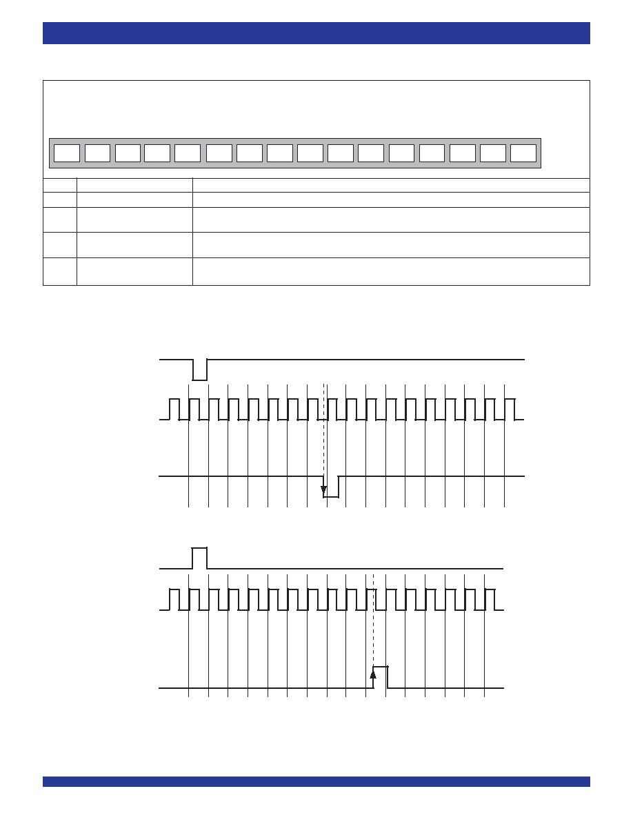
Frame
CLK
Offset Value
FE Input
0
1
2
3
4
5
6
7
8
9
10
11
12
13
14
15
GCI Frame
CLK
Offset Value
FE Input
(FD[10:0] = 06
H
)
(FD11 = 0, sample at CLK LOW phase)
(FD[10:0] = 09
H
)
(FD11 = 1, sample at CLK HIGH phase)
5712 drw07
TABLE 10
-- FRAME ALIGNMENT REGISTER (FAR) BITS
Figure 4. Example for Frame Alignment Measurement
Bit
Name
Description
15-13
Unused
Must be zero for normal operation.
12
CFE
When CFE = 1, the frame evaluation is completed and bits FD10 to FD0 bits contains a valid frame alignment
(Complete Frame Evaluation)
offset. This bit is reset to zero, when SFE bit in the IMS register is changed from 1 to 0.
11
FD11
The falling edge of FE (or rising edge for GCI mode) is sampled during the CLK-high phase (FD11 = 1)
(Frame Delay Bit 11)
or during the CLK-low phase (FD11 = 0). This bit allows the measurement resolution to Ω CLK cycle.
10-0
FD10-0
The binary value expressed in these bits refers to the measured input offset value. These bits are rest to
(Frame Delay Bits)
zero when the SFE bit of the IMS register changes from 1 to 0. (FD10 ≠ MSB, FD0 ≠ LSB)
Read/Write Address:
02
H
,
Reset Value:
0000
H
.
15
14
13
12
11
10
9
8
7
6
5
4
3
2
1
0
0
0
0
CFE
FD11
FD10
FD9
FD8
FD7
FD6
FD5
FD4
FD3
FD2
FD1
FD0

14
COMMERCIAL TEMPERATURE RANGE
IDT72V90823 3.3V TIME SLOT INTERCHANGE
DIGITAL SWITCH 2,048 x 2,048
TABLE 11
-- FRAME INPUT OFFSET REGISTER (FOR) BITS
NOTE:
1. n denotes an input stream number from 0 to 15.
Name
(1)
Description
OFn2, OFn1, OFn0
These three bits define how long the serial interface receiver takes to recognize and store bit 0 from the RX input pin: i.e., to
(Offset Bits 2, 1 & 0)
start a new frame. The input frame offset can be selected to +4.5 clock periods from the point where the external frame pulse
input signal is applied to the
F0i input of the device. See Figure 5.
DLEn
(Data Latch Edge)
ST-BUS
Æ
mode:
DLEn = 0, if clock rising edge is at the æ point of the bit cell.
DLEn = 1, if when clock falling edge is at the æ of the bit cell.
GCI mode:
DLEn = 0, if clock falling edge is at the æ point of the bit cell.
DLEn = 1, if when clock rising edge is at the æ of the bit cell.
Read/Write Address:
03
H
for FOR0 register,
04
H
for FOR1 register,
05
H
for FOR2 register,
06
H
for FOR3 register,
Reset Value:
0000
H
for all FOR registers.
15
14
13
12
11
10
9
8
7
6
5
4
3
2
1
0
OF32
OF31
OF30
DLE3
OF22
OF21
OF20
DLE2
OF12
OF11
OF10
DLE1
OF02
OF01
OF00
DLE0
FOR0 Register
15
14
13
12
11
10
9
8
7
6
5
4
3
2
1
0
OF72
OF71
OF70
DLE7
OF62
OF61
OF60
DLE6
OF52
OF51
OF50
DLE5
OF42
OF41
OF40
DLE4
FOR1 Register
15
14
13
12
11
10
9
8
7
6
5
4
3
2
1
0
OF112 OF111 OF110 DLE11 OF102 OF101 OF100 DLE10
OF92
OF91
OF90
DLE9
OF82
OF81
OF80
DLE8
FOR2 Register
15
14
13
12
11
10
9
8
7
6
5
4
3
2
1
0
OF152 OF151 OF150 DLE15 OF142 OF141 OF140 DLE14 OF132 OF131 OF130 DLE13 OF122 OF121 OF120 DLE12
FOR3 Register
15
COMMERCIAL TEMPERATURE RANGE
IDT72V90823 3.3V TIME SLOT INTERCHANGE
DIGITAL SWITCH 2,048 x 2,048
ST-BUS
F0i
RX Stream
5712 drw 08
Bit 7
Bit 7
CLK
Bit 7
Bit 7
denotes the 3/4 point of the bit cell
offset = 0,
DLE = 0
offset = 1,
DLE = 0
offset = 0,
DLE = 1
offset = 1,
DLE = 1
GCI
F0i
Bit 0
Bit 0
CLK
Bit 0
Bit 0
denotes the 3/4 point of the bit cell
offset = 0,
DLE = 0
offset = 1,
DLE = 0
offset = 0,
DLE = 1
offset = 1,
DLE = 1
RX Stream
RX Stream
RX Stream
RX Stream
RX Stream
RX Stream
RX Stream
TABLE 12
-- OFFSET BITS (OFN2, OFN1, OFN0, DLEN) & FRAME DELAY BITS
(FD11, FD2-0)
Figure 5. Examples for Input Offset Delay Timing
Measurement Result from
Corresponding
Input Stream
Frame Delay Bits
Offset Bits
Offset
FD11
FD2
FD1
FD0
OFn2
OFn1
OFn0
DLEn
No clock period shift (Default)
1
0
0
0
0
0
0
0
+ 0.5 clock period shift
0
0
0
0
0
0
0
1
+ 1.0 clock period shift
1
0
0
1
0
0
1
0
+ 1.5 clock period shift
0
0
0
1
0
0
1
1
+ 2.0 clock period shift
1
0
1
0
0
1
0
0
+ 2.5 clock period shift
0
0
1
0
0
1
0
1
+ 3.0 clock period shift
1
0
1
1
0
1
1
0
+ 3.5 clock period shift
0
0
1
1
0
1
1
1
+ 4.0 clock period shift
1
1
0
0
1
0
0
0
+ 4.5 clock period shift
0
1
0
0
1
0
0
1

16
COMMERCIAL TEMPERATURE RANGE
IDT72V90823 3.3V TIME SLOT INTERCHANGE
DIGITAL SWITCH 2,048 x 2,048
TABLE 13
-- CONNECTION MEMORY BITS
TABLE 14
-- CAB BIT PROGRAMMING FOR DIFFERENT DATA RATES
NOTE:
1. If bit 13 (PC) of the corresponding connection memory location is 1 (device in processor mode), then these entire 8 bits (SAB0, CAB6 - CAB0) are output on the output channel
and stream associated with this location.
Bit
Name
Description
15
LPBK
When 1, the RX n channel m data comes from the TX n channel m. For proper per channel loopback
(Per Channel Loopback)
operations, set the delay offset register bits OFn[2:0] to zero for the streams which are in the loopback mode.
14
V/C
This bit is used to select between the variable (LOW) and constant delay (HIGH) mode on a
(Variable/Constant
per-channel basis.
Throughput Delay)
13
PC
When 1, the contents of the connection memory are output on the corresponding output channel and stream.
(Processor Channel)
Only the lower byte (bit 7 ≠ bit 0) will be output to the TX output pins. When 0, the contents of the connection
memory are the data memory address of the switched input channel and stream.
12
CCO
This bit is output on the CCO pin one channel early. The CCO bit for stream 0 is output first.
(Control Channel Output)
11
OE
This bit enables the TX output drivers on a per-channel basis. When 1, the output driver functions
(Output Enable)
normally. When 0, the output driver is in a high-impedance state.
10-8,7
(1)
SAB3-0
The binary value is the number of the data stream for the source of the connection.
(Source Stream Address Bits)
6-0
(1)
CAB6-0
The binary value is the number of the channel for the source of the connection.
(Source Channel Address Bits)
15
14
13
12
11
10
9
8
7
6
5
4
3
2
1
0
LPBK
V/C
PC
CCO
OE
SAB3
SAB2
SAB1
SAB0
CAB6
CAB5
CAB4
CAB3
CAB2
CAB1
CAB0
Data Rate
CAB Bits Used to Determine the Source Channel of the Connection
2.048 Mb/s
CAB4 to CAB0 (32 channel/input stream)
4.096 Mb/s
CAB5 to CAB0 (64 channel/input stream)
8.192 Mb/s
CAB6 to CAB0 (128 channel/input stream)
17
COMMERCIAL TEMPERATURE RANGE
IDT72V90823 3.3V TIME SLOT INTERCHANGE
DIGITAL SWITCH 2,048 x 2,048
JTAG SUPPORT
The IDT72V90823 JTAG interface conforms to the Boundary-Scan stan-
dard IEEE-1149.1. This standard specifies a design-for-testability technique
called Boundary-Scan Test (BST). The operation of the boundary-scan
circuitry is controlled by an external test access port (TAP) Controller.
TEST ACCESS PORT (TAP)
The Test Access Port (TAP) provides access to the test functions of the
IDT72V90823. It consists of three input pins and one output pin.
∑Test Clock Input (TCK)
TCK provides the clock for the test logic. The TCK does not interfere with
any on-chip clock and thus remain independent. The TCK permits shifting of test
data into or out of the Boundary-Scan register cells concurrently with the
operation of the device and without interfering with the on-chip logic.
∑Test Mode Select Input (TMS)
The logic signals received at the TMS input are interpreted by the TAP
Controller to control the test operations. The TMS signals are sampled at the
rising edge of the TCK pulse. This pin is internally pulled to Vcc when it is not
driven from an external source.
∑Test Data Input (TDI)
Serial input data applied to this port is fed either into the instruction register
or into a test data register, depending on the sequence previously applied to
the TMS input. Both registers are described in a subsequent section. The
received input data is sampled at the rising edge of TCK pulses. This pin is
internally pulled to Vcc when it is not driven from an external source.
∑Test Data Output (TDO)
Depending on the sequence previously applied to the TMS input, the
contents of either the instruction register or data register are serially shifted out
towards the TDO. The data out of the TDO is clocked on the falling edge of the
TCK pulses. When no data is shifted through the boundary scan cells, the TDO
driver is set to a high impedance state.
∑Test Reset (
TRST)
Reset the JTAG scan structure. This pin is internally pulled to VCC.
INSTRUCTION REGISTER
In accordance with the IEEE 1149.1 standard, the IDT72V90823 uses
public instructions. The IDT72V90823 JTAG Interface contains a two-bit
instruction register. Instructions are serially loaded into the instruction register
from the TDI when the TAP Controller is in its shifted-IR state. Subsequently,
the instructions are decoded to achieve two basic functions: to select the test data
register that may operate while the instruction is current, and to define the serial
test data register path, which is used to shift data between TDI and TDO during
data register scanning. See Table below for Instruction decoding.
Value Instruction
Function
000 EXTEST
Select Boundary Scan Register
001 EXTEST
Select Boundary Scan Register
010 Sample/preload
Select Boundary Scan Register
011 Sample/preload
Select Boundary Scan Register
100 Sample/preload
Select Boundary Scan Register
101 Sample/preload
Select Boundary Scan Register
110 Bypass
Select Bypass Register
111 Bypass
Select Bypass Register
TEST DATA REGISTER
As specified in IEEE 1149.1, the IDT72V90823 JTAG Interface contains two
test data registers:
∑The Boundary-Scan register
The Boundary-Scan register consists of a series of Boundary-Scan cells
arranged to form a scan path around the boundary of the IDT72V90823 core
logic.
∑The Bypass Register
The Bypass register is a single stage shift register that provides a one-bit
path from TDI to its TDO. The IDT72V90823 boundary scan register contains
118 bits. Bit 0 in Table 15 Boundary Scan Register is the first bit clocked out.
All three-state enable bits are active high.
JTAG Instruction Register Decoding

18
COMMERCIAL TEMPERATURE RANGE
IDT72V90823 3.3V TIME SLOT INTERCHANGE
DIGITAL SWITCH 2,048 x 2,048
TABLE 15
-- BOUNDARY SCAN REGISTER BITS
Boundary Scan Bit 0 to bit 117
Device Pin
Three-State
Output
Input
Control
Scan Cell
Scan Cell
A4
76
A3
77
A2
78
A1
79
A0
80
WFPS
81
RESET
82
CLK
83
FE/HCLK
84
F0i
85
RX15
86
RX14
87
RX13
88
RX12
89
RX11
90
RX10
91
RX9
92
RX8
93
RX7
94
RX6
95
RX5
96
RX4
97
RX3
98
RX2
99
RX1
100
RX0
101
TX15
102
103
TX14
104
105
TX13
106
107
TX12
108
109
TX11
110
111
TX10
112
113
TX9
114
115
TX8
116
117
Boundary Scan Bit 0 to bit 117
Device Pin
Three-State
Output
Input
Control
Scan Cell
Scan Cell
TX7
0
1
TX6
2
3
TX5
4
5
TX4
6
7
TX3
8
9
TX2
10
11
TX1
12
13
TX0
14
15
ODE
16
CCO
17
18
DTA
19
D15
20
21
22
D14
23
24
25
D13
26
27
28
D12
29
30
31
D11
32
33
34
D10
35
36
37
D9
38
39
40
D8
41
42
43
AD7
44
45
46
AD6
47
48
49
AD5
50
51
52
AD4
53
54
55
AD3
56
57
58
AD2
59
60
61
AD1
62
63
64
AD0
65
66
67
IM
68
AD/ALE
69
CS
70
R/
W / WR
71
DS/
RD
72
A7
73
A6
74
A5
75

19
COMMERCIAL TEMPERATURE RANGE
IDT72V90823 3.3V TIME SLOT INTERCHANGE
DIGITAL SWITCH 2,048 x 2,048
RECOMMENDED DC OPERATING
CONDITIONS
DC ELECTRICAL CHARACTERISTICS
NOTE:
1.
Voltages are with respect to ground unless other wise stated.
NOTE:
1. Outputs Unloaded.
2. For TDI, TMS, and TRST pins, the maximum leakage current is 50
µA.
Test Point
Output
Pin
C
L
GND
S
1
R
L
VCC
GND
5712 drw09
S
2
Symbol
Parameter
Min.
Typ.
Max.
Units
V
CC
Positive Supply
3.0
3.6
V
V
IH
Input HIGH Voltage (3.3V)
2.0
V
CC
V
V
IH
Input HIGH Voltage (5.0V)
2.0
5.5
V
V
IL
Input LOW Voltage
GND
0.8
V
T
OP
Operating Temperature
-40
+85
∞C
Commercial
Symbol
Characteristics
Min.
Typ.
Max.
Units
I
CC
(1)
Supply Current
@ 2.048 Mb/s
7
10
mA
@ 4.096 Mb/s
14
20
mA
@ 8.192 Mb/s
30
45
mA
I
IL
(2)
Input Leakage (input pins)
15
µA
I
BL
Input Leakage (I/O pins)
50
µA
C
I
Input Pin Capacitance
10
pF
I
OZ
High-impedance Leakage
5
µA
V
OH
Output HIGH Voltage
2.4
V
V
OL
Output LOW Voltage
0.4
V
C
O
Output Pin Capacitance
10
pF
Figure 6. Output Load
S1 is open circuit except when testing output
levels or high impedance states.
S2 is switched to V
CC
or GND when testing
output levels or high impedance states.
Symbol
Parameter
Min.
Max.
Unit
V
CC
Supply Voltage
-0.3
5.0
V
Vi
Voltage on Digital Inputs (3.3V)
GND -0.3
V
CC
+0.3
V
Vi
Voltage on Digital Inputs (5.0V)
GND -0.3
5.5
V
I
O
Current at Digital Outputs
20
mA
T
S
Storage Temperature
-65
+125
∞ C
P
D
Package Power Dissapation
1
W
NOTE:
1. Exceeding these values may cause permanent damage. Functional operation under
these conditions is not implied.
ABSOLUTE MAXIMUM RATINGS
(1)
20
COMMERCIAL TEMPERATURE RANGE
IDT72V90823 3.3V TIME SLOT INTERCHANGE
DIGITAL SWITCH 2,048 x 2,048
AC ELECTRICAL CHARACTERISTICS - FRAME PULSE AND CLK
NOTE:
1. High Impedance is measured by pulling to the appropriate rail with R
L
, with timing corrected to cancel time taken to discharge C
L
.
Symbol
Characteristics
Min.
Typ.
Max.
Units
t
FPW
Frame Pulse Width (ST-BUS
Æ
, GCI)
Bit rate = 2.048 Mb/s
26
295
ns
Bit rate = 4.096 Mb/s
26
145
ns
Bit rate = 8.192 Mb/s
26
80
ns
t
FPS
Frame Pulse Setup time before CLK falling (ST-BUS
Æ
or GCI)
5
ns
t
FPH
Frame Pulse Hold Time from CLK falling (ST-BUS
Æ
or GCI)
10
ns
t
CP
CLK Period
Bit rate = 2.048 Mb/s
190
300
ns
Bit rate = 4.096 Mb/s
110
150
ns
Bit rate = 8.192 Mb/s
55
70
ns
t
CH
CLK Pulse Width HIGH
Bit rate = 2.048 Mb/s
85
150
ns
Bit rate = 4.096 Mb/s
50
75
ns
Bit rate = 8.192 Mb/s
20
40
ns
t
CL
CLK Pulse Width LOW
Bit rate = 2.048 Mb/s
85
150
ns
Bit rate = 4.096 Mb/s
50
75
ns
Bit rate = 8.192 Mb/s
20
40
ns
t
r
, t
f
Clock Rise/Fall Time
10
ns
t
HFPW
Wide Frame Pulse Width
Bit rate = 8.192 Mb/s
195
295
ns
t
HFPS
Frame Pulse Setup Time before HCLK falling
5
150
ns
t
HFPH
Frame Pulse Hold Time from HCLK falling
10
150
ns
t
HCP
HCLK (4.096 MHz) Period
Bit rate = 8.192 Mb/s
190
300
ns
t
HCH
HCLK (4.096 MHz) Pulse Width HIGH
Bit rate = 8.192 Mb/s
85
150
ns
t
HCL
HCLK (4.096 MHz) Pulse Width LOW
Bit rate = 8.192 Mb/s
85
150
ns
t
Hr
, t
Hf
HCLK Rise/Fall Time
10
ns
t
DIF
Delay between falling edge of HCLK and falling edge of CLK
-10
10
ns
Symbol
Characteristics
Min.
Typ.
Max.
Unit
Test Conditions
t
SIS
RX Setup Time
0
ns
t
SIH
RX Hold Time
10
ns
t
SOD
TX Delay ≠ Active to Active
30
ns
C
L
= 30pF
40
ns
C
L
= 200pF
t
DZ
TX Delay ≠ Active to High-Z
32
ns
R
L
= 1K
, C
L
= 200pF
t
ZD
TX Delay ≠ High-Z to Active
32
ns
R
L
= 1K
, C
L
= 200pF
t
ODE
Output Driver Enable (ODE) Delay
32
ns
R
L
= 1K
, C
L
= 200pF
t
XCD
CCO Output Delay
30
ns
C
L
= 30pF
40
ns
C
L
= 200pF
AC ELECTRICAL CHARACTERISTICS - SERIAL STREAMS
(1)
21
COMMERCIAL TEMPERATURE RANGE
IDT72V90823 3.3V TIME SLOT INTERCHANGE
DIGITAL SWITCH 2,048 x 2,048
Bit 1, Channel 0
Bit 0, Channel 0
Bit 7, Last Ch
(1)
Bit 2, Channel 0
Bit 1, Channel 0
Bit 0, Channel 0
Bit 7, Last Ch
(1)
Bit 2, Channel 0
t
FPW
t
FPH
t
CH
t
CL
t
f
t
r
t
FPS
t
SOD
t
SIS
t
SIH
F0i
CLK
TX
RX
t
CP
5712 drw11
NOTE:
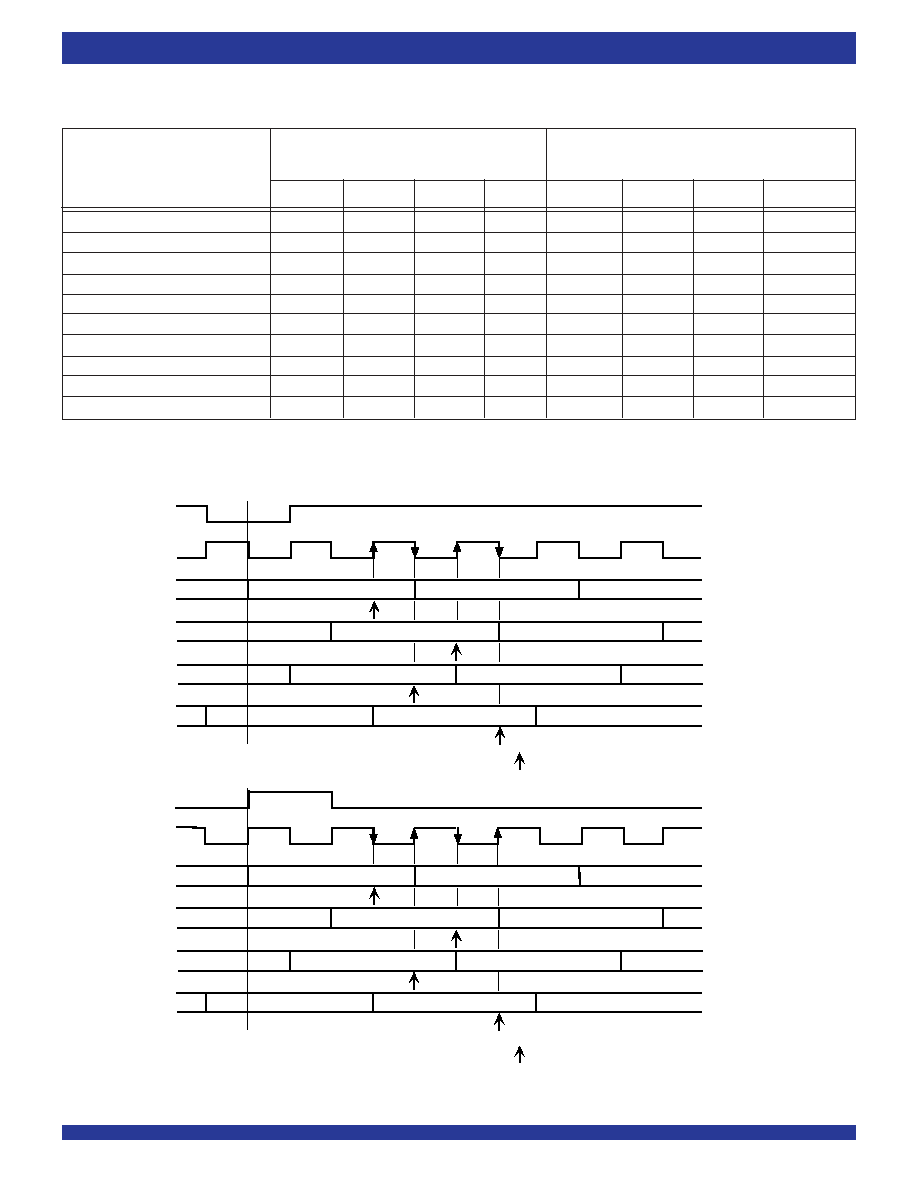
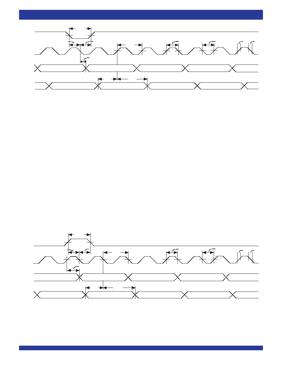
1. 2.048 Mb/s mode, last channel = ch 31,
4.096 Mb/s mode, last channel = ch 63,
8.192 Mb/s mode, last channel = ch 127.
Figure 8. GCI Timing at 2.048 Mb/s and High Speed Serial Interface at 4.096 Mb/s or 8.192 Mb/s, when WFPS pin = 0
t
FPW
t
FPH
t
CH
t
CL
t
f
t
r
t
FPS
t
SOD
t
SIS
t
SIH
F0i
CLK
TX
RX
t
CP
5712 drw10
Bit 6, Channel 0
Bit 7, Channel 0
Bit 0, Last Ch
(1)
Bit 5, Channel 0
Bit 6, Channel 0
Bit 7, Channel 0
Bit 0, Last Ch
(1)
Bit 5, Channel 0
NOTE:
1. 2.048 Mb/s mode, last channel = ch 31,
4.096 Mb/s mode, last channel = ch 63,
8.192 Mb/s mode, last channel = ch 127.
Figure 7. ST-BUS
Æ
Timing for 2.048 Mb/s and High Speed Serial Interface at 4.096 Mb/s or 8.192 Mb/s, when WFPS pin = 0.

22
COMMERCIAL TEMPERATURE RANGE
IDT72V90823 3.3V TIME SLOT INTERCHANGE
DIGITAL SWITCH 2,048 x 2,048
t
XCD
t
ZD
CLK
(ST-BUS
or
WFPS mode)
CLK
(GCI mode)
CCO
5712 drw13
TX
TX
VALID DATA
VALID DATA
t
DZ
t
ODE
ODE
TX
VALID DATA
5712 drw14
t
ODE
Figure 10. Serial Output and External Control
Figure 11. Output Driver Enable (ODE)
t
HFPH
t
DIF
F0i
TX
RX
5712 drw12
Bit 1, Ch 127
Bit 0, Ch 127
Bit 7, Ch 0
Bit 6, Ch 0
Bit 5, Ch 0
Bit 4, Ch 0
Bit 1, Ch 127
Bit 0, Ch 127
Bit 7, Ch 0
Bit 6, Ch 0
Bit 5, Ch 0
Bit 4, Ch 0
t
HFPS
t
HFPW
CLK
16.384 MHz
HCLK
4.096 MHz
t
HCH
t
HCP
t
CP
t
CH
t
CL
t
r
t
SOD
t
f
t
SIS
t
SIH
t
HCL
t
Hf
t
Hr
Figure 9. WFP Bus Timing for High Speed Serial Interface (8.192 Mb/s), when WFPS pin = 1
NOTE:
1. High Impedance is measured by pulling to the appropriate rail with R
L
, with timing corrected to cancel time taken to discharge C
L
.

23
COMMERCIAL TEMPERATURE RANGE
IDT72V90823 3.3V TIME SLOT INTERCHANGE
DIGITAL SWITCH 2,048 x 2,048
t
ALW
ALE
5712 drw15
ADDRESS
DATA
t
RW
t
WW
t
CSRW
t
ALRD
t
CSR
t
CSW
t
DHW
t
DHR
t
AKH
t
DDR
t
DSW
t
SWD
t
ALWR
t
AKD
AD0-AD7
D8-D15
CS
RD
WR
DTA
t
ADS
t
ADH
Figure 12. Multiplexed Bus Timing (Intel Mode)
AC ELECTRICAL CHARACTERISTICS - MULTIPLEXED BUS TIMING (INTEL)
NOTE:
1. High Impedance is measured by pulling to the appropriate rail with R
L
, with timing corrected to cancel time taken to discharge C
L
.
Symbol
Parameter
Min.
Typ.
Max.
Units
Test Conditions
t
ALW
ALE Pulse Width
20
ns
t
ADS
Address Setup from ALE falling
3
ns
t
ADH
Address Hold from ALE falling
3
ns
t
ALRD
RD Active after ALE falling
3
ns
t
DDR
Data Setup from
DTA LOW on Read
5
ns
C
L
= 150pF
t
CSRW
CS Hold after RD/WR
5
ns
t
RW
RD Pulse Width (Fast Read)
45
ns
t
CSR
CS Setup from RD
0
ns
t
DHR
(1)
Data Hold after
RD
10
20
ns
C
L
= 150pF, R
L
= 1K
t
WW
WR Pulse Width (Fast Write)
45
ns
t
ALWR
WR Delay after ALE falling
3
ns
t
CSW
CS Setup from WR
0
ns
t
DSW
Data Setup from
WR (Fast Write)
20
ns
t
SWD
Valid Data Delay on Write (Slow Write)
122
ns
t
DHW
Data Hold after
WR Inactive
5
ns
t
AKD
Acknowledgment Delay:
Reading/Writing Registers
43/43
ns
C
L
= 150pF
Reading/Writing Memory
@ 2.048 Mb/s
760/750
ns
C
L
= 150pF
@ 4.096 Mb/s
400/390
ns
C
L
= 150pF
@ 8.192 Mb/s
220/210
ns
C
L
= 150pF
t
AKH
(1)
Acknowledgment Hold Time
22
ns
C
L
= 150pF, R
L
= 1K

24
COMMERCIAL TEMPERATURE RANGE
IDT72V90823 3.3V TIME SLOT INTERCHANGE
DIGITAL SWITCH 2,048 x 2,048
DS
5712 drw16
ADDRESS
t
CSS
t
DSH
t
ASW
t
CSH
t
DDR
t
ADS
t
ADH
AD0-AD7,
D8-D15
WR
CS
DTA
DATA
ADDRESS
DATA
t
RWS
t
DWS
t
SWD
t
DHW
t
AKD
AD0-AD7,
D8-D15
RD
R/
W
AS
t
RWH
t
AKH
t
DHR
AC ELECTRICAL CHARACTERISTICS - MULTIPLEXED BUS TIMING (MOTOROLA)
Figure 13. Multiplexed Bus Timing (Motorola Mode)
Symbol
Parameter
Min.
Typ.
Max.
Units
Test Conditions
t
ASW
ALE Pulse Width
20
ns
t
ADS
Address Setup from AS falling
3
ns
t
ADH
Address Hold from AS falling
3
ns
t
DDR
Data Setup from
DTA LOW on Read
5
ns
C
L
= 150pF
t
CSH
CS Hold after DS falling
0
ns
t
CSS
CS Setup from DS rising
0
ns
t
DHW
Data Hold after Write
5
ns
t
DWS
Data Setup from DS ≠ Write (Fast Write)
20
ns
t
SWD
Valid Data Delay on Write (Slow Write)
122
ns
t
RWS
R/
W Setup from DS Rising
60
ns
t
RWH
R/
W Hold from DS Rising
5
ns
t
DHR
(1)
Data Hold after Read
10
20
ns
C
L
= 150pF, R
L
= 1K
t
DSH
DS Delay after AS falling
10
ns
t
AKD
Acknowledgment Delay:
Reading/Writing Registers
43/43
ns
C
L
= 150pF
Reading/Writing Memory
@ 2.048 Mb/s
760/750
ns
C
L
= 150pF
@ 4.096 Mb/s
400/390
ns
C
L
= 150pF
@ 8.192 Mb/s
220/210
ns
C
L
= 150pF
t
AKH
(1)
Acknowledgment Hold Time
22
ns
C
L
= 150pF, R
L
= 1K
NOTE:
1. High Impedance is measured by pulling to the appropriate rail with R
L
, with timing corrected to cancel time taken to discharge C
L
.
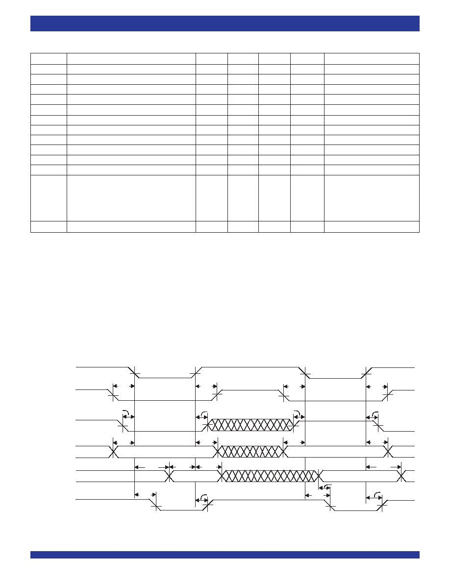
25
COMMERCIAL TEMPERATURE RANGE
IDT72V90823 3.3V TIME SLOT INTERCHANGE
DIGITAL SWITCH 2,048 x 2,048
DS
CS
VALID WRITE ADDRESS
A0-A7
t
CSS
t
CSH
R/
W
t
RWS
t
RWH
t
ADS
t
ADH
VALID WRITE
DATA
AD0-AD7/
D8-D15
t
DSW
t
DHW
DTA
t
AKD
t
AKH
t
CSS
t
CSH
t
RWS
t
RWH
VALID READ ADDRESS
t
ADS
t
ADH
VALID READ DATA
t
DDR
t
DHR
t
AKD
t
AKH
5712 drw17
t
SWD
Figure 14. Motorola Non-Multiplexed Asyncronous Bus Timing
AC ELECTRICAL CHARACTERISTICS-MOTOROLA NON-MULTIPLEXED BUS MODE
Symbol
Parameter
Min.
Typ.
Max.
Units
Test Conditions
t
CSS
CS Setup from DS falling
0
ns
t
RWS
R/W Setup from DS falling
10
ns
t
ADS
Address Setup from DS falling
2
ns
t
CSH
CS Hold after DS rising
0
ns
t
RWH
R/W Hold after DS Rising
2
ns
t
ADH
Address Hold after DS Rising
2
ns
t
DDR
Data Setup from DTA LOW on Read
2
ns
C
L
= 150pF
t
DHR
Data Hold on Read
10
20
ns
C
L
= 150pF, R
L
= 1K
t
DSW
Data Setup on Write (Fast Write)
5
ns
t
SWD
Valid Data Delay on Write (Slow Write)
122
ns
t
DHW
Data Hold on Write
5
ns
t
AKD
Acknowledgment Delay:
Reading/Writing Registers
43/43
ns
C
L
= 150pF
Reading/Writing Memory
@ 2.048 Mb/s
760/750
ns
C
L
= 150pF
@ 4.096 Mb/s
400/390
ns
C
L
= 150pF
@ 8.192 Mb/s
220/210
ns
C
L
= 150pF
t
AKH
(1)
Acknowledgment Hold Time
22
ns
C
L
= 150pF, R
L
= 1K
NOTE:
1. High Impedance is measured by pulling to the appropriate rail with R
L
, with timing corrected to cancel time taken to discharge C
L
.

26
COMMERCIAL TEMPERATURE RANGE
IDT72V90823 3.3V TIME SLOT INTERCHANGE
DIGITAL SWITCH 2,048 x 2,048
5712 drw18
AD0-AD7/
D8-D15
CS
DTA
VALID WRITE
ADDRESS
R/
W
A0-A7
DS
CLK GCI
CLK ST-BUS
t
DSS
t
CSS
t
CSH
t
RWS
t
RWH
VALID READ
ADDRESS
t
ADS
t
ADH
VALID READ
DATA
t
DHR
t
CKAK
t
AKH
t
DDR
t
DSPW
t
DSS
t
CSS
t
CSH
t
RWS
t
RWH
t
ADS
t
ADH
VALID WRITE
DATA
t
SWD
t
DHW
t
CKAK
t
AKH
Figure 15. Motorola Non-Multiplexed Syncronous Bus Timing

27
CORPORATE HEADQUARTER for SALES:
for Tech Support:
2975 Stender Way
800-345-7015 or 408-727-6116
408-330-1753
Santa Clara, CA 95054
fax: 408-492-8674
email: FIFOhelp@idt.com
www.idt.com
5712 drw19
XXXXXX
IDT
Device Type
X
Package
Process/
Temperature
Range
XX
BLANK
Commercial (-40
∞C to +85∞C)
72V90823
2,048 x 2,048
3.3V Time Slot Interchange Digital Switch
J
BC
PQF
PF
Plastic Leaded Chip Carrier (PLCC, J84-1)
Ball Grid Array (BGA, BC100-1)
Plastic Quad Flatpack (PQFP, PQ100-2)
Thin Quad Flat Pack (TQFP, PN100-1)
ORDERING INFORMATION
DATASHEET DOCUMENT HISTORY
5/19/2000
pgs. 1,3,18 and 25.
7/27/2000
pgs. 1, 2, 4, 5, 6, 7, 16 and 25.
8/14/2000
pg. 6.
9/14/2000
pgs. 2, 3, 12, 13 and 18.
1/02/2001
pgs. 7, 18, 21, 22, 23, and 24
1/25/2001
pgs. 1, 16, 18 and 24.
5/16/2001
pg. 16
08/06/2001
pgs. 4, 5, 12 and 25.
12/18/2002
pg. 3