
1
IDT7381
16-BIT CASCADABLE ALU
COMMERCIAL TEMPERATURE RANGE
APRIL 2001
2001 Integrated Device Technology, Inc.
DSC-2525/-
c
IDT7381
COMMERCIAL TEMPERATURE RANGE
16-BIT CMOS
CASCADABLE ALU
FUNCTIONAL BLOCK DIAGRAM
DESCRIPTION:
The IDT7381 is a high-speed cascadable Arithmetic Logic Unit (ALU).
These three-bus devices have two input registers, an ultra-fast 16-bit ALU
and 16-bit output register. With IDT's high-performance CMOS technology,
the IDT7381 can do arithmetic or logic operations in 25ns. The IDT7381
functionally replaces four 54/74S381 four-bit ALUs in a 68-pin package.
The two input operands, A and B, can be clocked or fed through for
flexible pipelining. The F output can also be set into clocked or flow-through
mode. An output enable is provided for three-state control of the output port
on a bus.
The IDT7381 has three function pins to select 1 of 8 arithmetic or logic
operations. The two R and S selection pins determine whether A, B, F or
0 are fed into the ALU. This ALU has carry-out, propagate and generate
outputs for cascading using carry look-ahead.
A
0 - 15
B
0 - 1 5
16
A R EG
B R EG
A M U X
B M U X
R M U X
S M U X
F RE G
F M UX
PO W E R
SU P P LY
CL K
E N B
FT AB
FTF
G N D
V
C C
16
2
3
16
RS
0 - 1
I
0 - 2
E N A
EN F
P
G
O E
C
1 6
O VF
Z
F
0 - 15
C
0
16-BIT AL U
0000 H
0000 H
FEATURES:
- High-performance 16-bit Arithmetic Logic Unit (ALU)
- 25ns to 55ns clocked ALU operations
- Ideal for radar, sonar or image processing applications
- 74S381 instruction set (8 functions)
- Replaces Gould S614381 or Logic Devices L4C381
- Cascadable with or without carry look-ahead
- Pipeline or flow-through modes
- Internal feedback path for accumulation
- Three-state outputs
- TTL-compatible
- Produced with advanced submicron CMOS technology
- Available in PLCC
- Speeds available: L/25/30/40/55
The IDT logo is a registered trademark of Integrated Device Technology, Inc.

2
COMMERCIAL TEMPERATURE RANGE
IDT7381
16-BIT CASCADABLE ALU
PIN CONFIGURATION
10
11
12
13
14
15
16
17
18
19
20
21
22
23
24
25
26
27 28 29 30 31 32 33 34 35 36 37 38 39 40 41 42 43
60
59
58
57
56
55
54
53
52
51
50
49
48
47
46
45
44
9
8
7
6
5
4
3
2
1 68 67 66 65 64 63 62 61
B
7
B
6
B
5
B
4
B
3
B
2
B
1
B
0
E N A
E N B
FT AB
RS
1
RS
0
I
2
I
1
I
0
C
0
A
9
A
1 0
A
1 1
A
1 2
A
1 3
A
1 4
A
1 5
CL K
V
C C
G N D
C
16
P
G
Z
O VF
EN F
FTF
A
8
A
7
A
6
A
5
A
4
A
3
A
2
A
1
A
0
B
1
5
B
1
4
B
1
3
B
1
2
B
1
1
B
1
0
B
9
B
8
J68 - 1
O
E
F
1
5
F
1
4
F
1
3
F
1
2
F
1
1
F
1
0
F
9
F
8
F
7
F
6
F
5
F
4
F
3
F
2
F
1
F
0
Pin 1
Desig nato r
PLCC
TOP VIEW
3
IDT7381
16-BIT CASCADABLE ALU
COMMERCIAL TEMPERATURE RANGE
PIN DESCRIPTION
Pin Name
I/O
Description
A
0
- A
15
I
Sixteen�bit data input port.
B
0
- B
15
I
Sixteen�bit data input port.
ENA
I
Register enable for the A input port; active low pin.
ENB
I
Register enable for the B input port; active low pin.
FTAB
I
Flow�through control pin. When this pin is high, both register A and B are transparent.
F
0
� F
15
O
Sixteen�bit data output port.
ENF
I
Register enable for the F output port; active low pin.
FTF
I
Flow�through control pin. When this pin is high, the F register is transparent.
CLK
I
Clock input.
OE
I
Output enable control pin. When this pin is high, the output port F is in a high impedance state. When low, the output
port F is active.
C
0
I
Carry input. This pin receives arithmetic carries from less significant ALU components in a cascade
configuration.
C
16
O
Carry output. This pin produces arithmetic carries to more significant ALU components in a cascaded
configuration.
OVF
O
This pin indicates a two's complement arithmetic overflow, when high.
Z
O
This pin indicates a zero output result, when high.
RS
0
� RS
1
I
Two control pins used to select input operands for the R and S multiplexers.
I
0
- I
2
I
Three control pins to select the ALU function performed.
P
O
Indicates the carry propagate output state to the ALU.
G
O
Indicates the carry generate output state to the ALU.
V
CC
Power supply pin, 5V.
GND
Ground pin, 0V.
R AND S MUX TABLE
RS
1
RS
0
R Mux
S Mux
0
0
A
F
0
1
A
0
1
0
0
B
1
1
A
B
ALU FUNCTION TABLE
I
2
I
1
I
0
Function
0
0
0
F = 0
0
0
1
F = R + S + C
0
0
1
0
F = R + S + C
0
0
1
1
F = R + S + C
0
1
0
0
F = R xor S
1
0
1
F = R or S
1
1
0
F = R and S
1
1
1
F = all 1's

4
COMMERCIAL TEMPERATURE RANGE
IDT7381
16-BIT CASCADABLE ALU
ABSOLUTE MAXIMUM RATINGS
(1)
Symbol
Description
Max.
Unit
V
TERM
Terminal Voltage with
�0.5 to
V
Respect to Ground
V
CC
+ 0.5
V
CC
Power Supply Voltage
�0.5 to +7.0
V
T
STG
Storage Temperature
�55 to +125
�C
I
OUT
DC Output Current
50
mA
NOTE:
1. Stresses greater than those listed under ABSOLUTE MAXIMUM RAT-
INGS may cause permanent damage to the device. This is a stress rating
only and functional operation of the device at these or any other conditions
above those indicated in the operational sections of this specification is
not implied. Exposure to absolute maximum rating conditions for extended
periods may affect reliability. Under no circumstances should an input
of an I/O Pin be greater than V
CC
+ 0.5V.
CAPACITANCE
(T
A
= +25�C, f = 1.0MHz)
Symbol
Parameter
(1)
Conditions
Pkg.
Typ.
Unit
C
IN
Input Capacitance
V
IN
= 0V
PGA
10
pF
PLCC
5
C
OUT
Output Capacitance
V
OUT
= 0V
PGA
12
pF
PLCC
7
NOTE:
1. This parameter is sampled at initial characterization and is not production
tested.
DC ELECTRICAL CHARACTERISTICS
Commercial: T
A
= 0�C to +70�C, V
CC
= 5.0V � 5%
Symbol
Parameter
Test Conditions
(1)
Min.
Typ.
(2)
Max.
Unit
V
IH
Input HIGH Level
Guaranteed Logic HIGH Level
2
--
--
V
V
IL
Input LOW Level
Guaranteed Logic LOW Level
--
--
0.8
V
I
IH
Input HIGH Current
V
CC
= Max., V
IN
= 2.7V
--
--
10
�A
I
IL
Input LOW Current
V
CC
= Max., V
IN
= 0.5V
--
--
�10
�A
I
OS(3)
Short Circuit Current
V
CC
= Max., V
OUT
= GND
�20
--
�100
mA
I
OZ
Off State (High Impedance)
V
CC
= Max.
V
O
= 0.5V
--
�0.1
�20
�A
Output Current
V
O
= 2.7V
--
�0.1
20
V
OH
Output HIGH Voltage
V
CC
= Min.
I
OH
= �4mA
2.4
--
--
V
V
IN
= V
IH
or V
IL
V
OL
Output LOW Voltage
V
CC
= Min.
I
OL
= 8mA
--
--
0.5
V
V
IN
= V
IH
or V
IL
NOTES:
1. For conditions shown as Max. or Min., use appropriate value specified under Electrical Characteristics for the applicable device type.
2. Typical values are at V
CC
= 5.0V, +25�C ambient and maximum loading.
3. Not more than one output should be shorted at one time. Duration of the short circuit test should not exceed one second.

5
IDT7381
16-BIT CASCADABLE ALU
COMMERCIAL TEMPERATURE RANGE
POWER SUPPLY CHARACTERISTICS
Commercial: T
A
= 0�C to +70�C, V
CC
= 5.0V � 5%
Symbol
Parameter
Test Conditions
(1)
Min.
Typ.
(2)
Max.
Unit
I
CC
Quiescent Power Supply Current
V
CC
= Max.
--
2
6
mA
V
IN
=GND or V
CC
I
CC
(3)
Quiescent Power Supply Current
V
CC
= Max.
--
0.5
1
mA/
TTL Input HIGH
V
IN
= 3.4V
input
I
CCD
(4)
Dynamic Power Supply Current
V
CC
= Max.
--
15
48
�A/
Outputs disabled
MHz
V
IN
= GND or V
CC
Mode: FTAB = FTF = 1
I
CCD1
Dynamic Power Supply Current
V
CC
= Max.
--
20
33
mA
Outputs Disabled
All Data Inputs Disabled
f
i
= 10MHz, f
CP
= 10MHz
50% Duty Cycle
V
IL
= GND, V
IH
= V
CC
Mode: FTAB = FTF = 1
I
CCD2
(6)
Dynamic Power Supply Current
V
CC
= Max.
--
40
60
mA
Outputs Enabled. (CL = 50pF)
All Data Inputs Sw itching
f
i
= 10MHz, f
CP
= 10MHz
50% Duty Cycle
V
IL
= GND, V
IH
= V
CC
Mode: FTAB = FTF = 1
I
C
(7)
Total Power Supply Current
V
CC
= Max.
Outputs Disabled
--
22
39
mA
V
IN
= GND or V
CC
All Data Inputs Switching
f
i
= 10MHz, f
CP
= 10MHz
Outputs Enabled
--
42
76
mA
50% Duty Cycle
NOTES:
1. For conditions shown as Max. or Min., use appropriate value specified under Electrical Characteristics for the applicable device type.
2. Typical values are at V
CC
= 5.0V, +25�C ambient.
3. Per TTL driven input (V
IN
= 3.4V); all other inputs at V
CC
or GND.
4. This parameter is not directly testable, but is derived from I
CCD1
for use in Total Power Supply calculations.
5. Total power supply current is calculated as follows:
I
C
= I
QUIESCENT
+ I
INPUTS
+ I
DYNAMIC
I
C
= I
CC
+
I
CC
D
H
N
T
+ I
CCD
(f
CP
+ f
i
N
i
)
I
CC
= Quiescent Current
I
CC
= Power Supply Current for a TTL High Input (V
IN
= 3.4V)
D
H
= Duty Cycle for TTL Inputs High
N
T
= Number of TTL Inputs at D
H
I
CCD
= Dynamic Current Caused by an Output Transition Pair (HLH or LHL)
f
CP
= Clock Frequency for Register Devices (Zero for Non-Register Devices)
f
i
= Input Frequency
N
i
= Number of Inputs at f
i
All currents are in milliamps and all frequencies are in megahertz.
6. This parameter is not production tested but is an indicator of the power dissipated with outputs loaded.
7. Values for these conditions are examples of the I
C
formula in note 5 above. These are guaranteed but not tested.
6
COMMERCIAL TEMPERATURE RANGE
IDT7381
16-BIT CASCADABLE ALU
AC ELECTRICAL CHARACTERISTICS
(V
CC
= 5V � 5%, T
A
= 0�C to +70�C)
NOTES:
1. Only for FTF = 0.
2. Minimum propagation delays are not production tested but guaranteed to be greater than or equal to 3ns.
Maximum Combinational Propagation Delays
IDT7381L25
IDT7381L30
From Input
F
0�15
P, G, N
Z,OVF
C
16
F
0�15
P, G, N
Z,OVF
C
16
Unit
FTAB = 0, FTF = 0
CLK
13
22
26
22
20
28
30
28
ns
C
0
--
--
16
16
--
--
20
20
ns
I
0�2
, RS
0
, RS
1
--
22
22
22
--
28
28
28
ns
FTAB = 0, FTF = 1
CLK
27
22
26
22
33
28
30
28
ns
C
0
22
--
16
16
28
--
20
20
ns
I
0�2
, RS
0
, RS
1
22
22
22
22
28
28
28
28
ns
FTAB = 1, FTF = 0
A
0
�A
15
, B
0
�B
15
--
18
25
22
--
24
30
28
ns
CLK
13
--
--
--
19
--
--
--
ns
C
0
--
--
16
16
--
--
20
20
ns
I
0�2
, RS
0
, RS
1
--
22
22
22
--
28
28
28
ns
FTAB = 1, FTF = 1
A
0
�A
15
, B
0
�B
15
26
18
25
22
32
24
30
28
ns
C
0
22
--
16
16
28
--
20
20
ns
I
0�2
, RS
0
, RS
1
22
22
22
22
28
28
28
28
ns
Maximum Combinational Propagation Delays
IDT7381L40
IDT7381L55
From Input
F
0�15
P, G, N
Z,OVF
C
16
F
0�15
P, G, N
Z,OVF
C
16
Unit
FTAB = 0, FTF = 0
CLK
26
30
44
32
32
38
53
36
ns
C
0
--
--
28
20
--
--
34
22
ns
I
0�2
, RS
0
, RS
1
--
32
34
35
--
42
42
42
ns
FTAB = 0, FTF = 1
CLK
46
30
44
32
56
38
53
36
ns
C
0
30
--
28
20
37
--
34
22
ns
I
0�2
, RS
0
, RS
1
40
32
34
35
55
42
42
42
ns
FTAB = 1, FTF = 0
A
0
�A
15
, B
0
�B
15
--
30
40
32
--
36
46
37
ns
CLK
26
--
--
--
32
--
--
--
ns
C
0
--
--
28
20
--
--
34
22
ns
I
0�2
, RS
0
, RS
1
--
32
34
35
--
42
42
42
ns
FTAB = 1, FTF = 1
A
0
�A
15
, B
0
�B
15
40
30
40
32
55
36
46
37
ns
C
0
30
--
28
20
37
--
34
22
ns
I
0�2
, RS
0
, RS
1
40
32
34
35
55
42
42
42
ns

7
IDT7381
16-BIT CASCADABLE ALU
COMMERCIAL TEMPERATURE RANGE
AC ELECTRICAL CHARACTERISTICS
(V
CC
= 5V � 5%, T
A
= 0�C to +70�C) - (Cont'd.)
NOTES:
1. Only for FTF = 0.
2. Minimum propagation delays are not production tested but guaranteed to be greater than or equal to 3ns.
Minimum Set-up and Hold Times Relative to Clock (CLK)
IDT7381L25
IDT7381L30
IDT7381L40
IDT7381L55
Input
Set-up
Hold
Set-up
Hold
Set-up
Hold
Set-up
Hold
Unit
FTAB = 0, FTF = X
A
0
�A
15
, B
0
�B
15
6
0
6
0
6
0
8
0
ns
C
0
(1)
16
0
16
0
16
0
21
0
ns
I
0�2
, RS
0
, RS
1
(1)
24
0
29
0
32
0
44
0
ns
ENA, ENB, ENF
6
0
6
0
6
0
8
0
ns
FTAB = 1, FTF = 0
A
0
�A
15
, B
0
�B
15
16
0
25
0
28
0
35
0
ns
C
0
16
0
16
0
16
0
21
0
ns
I
0�2
, RS
0
, RS
1
24
0
29
0
32
0
44
0
ns
ENF
6
0
6
0
6
0
8
0
ns
Minimum Clock Cycle Times and Pulse Widths
Parameter
IDT7381L25
IDT7381L30
IDT7381L40
IDT7381L55
Unit
Clock LOW Time
6
8
10
14
ns
Clock HIGH Time
6
8
10
14
ns
Clock Period
20
25
34
43
ns
Maximum Output Enable/Disable Times
Parameter
IDT7381L25
IDT7381L30
IDT7381L40
IDT7381L55
Unit
Enable Time
10
15
18
20
ns
Disable Time
10
15
18
20
ns
8
COMMERCIAL TEMPERATURE RANGE
IDT7381
16-BIT CASCADABLE ALU
WAVEFORMS FOR FTAB = 0, FTF = X
Prop. 1
Prop. 1
Prop. 1
Prop. 1
Prop. 2
Prop. 2
Prop. 2
Prop. 2
Prop. 3
Prop. 3
Prop. 3
Prop. 1
Enable
Enable
Disable
Disable
Result
Result
Result
Result
Result
Hold
Set-up
Hold
Set-up
Hold
Set-up
Hold
Set-up
CLK
A
0- 15
B
0- 15
C
0
I
0- 2
,
ENA, ENB
ENF
O E
F
0- 15
(FTF = 0)
F
0- 15
(FTF = 1)
Prop. 1: Propagation delay with respect to the CLK.
Prop. 2: Propagation delay with respect to I
0- 2
, RS
0- 2.
Prop. 3: Propagation delay with respect to C0.
DATA 2
DATA 3
T1
T2
DATA 3
DATA 2
DATA 3
DATA 2
DATA 2
DATA 3
DATA 1
DATA 1
DATA 1
DATA 1
RS
0- 1
P
,
G
Z, O VF
C
16

9
IDT7381
16-BIT CASCADABLE ALU
COMMERCIAL TEMPERATURE RANGE
WAVEFORMS FOR FTAB = 1, FTF = X
Prop. 4 (For FTF = 1 only)
Prop. 4 (for FTF = 1 only)
Prop. 2
Prop. 2
Prop. 2
Prop. 2
Prop. 3
Prop. 3
Prop. 3
Prop. 1
Enable
Enable
Disable
Disable
Result
Result
Result
Result
Result
Hold
Set-up
Hold
Set-up
Hold
Set-up
Hold
Set-up
Prop. 4
DATA 2
DATA 3
T1
T2
DATA 3
DATA 2
DATA 3
DATA 2
DATA 2
DATA 3
DATA 1
DATA 1
DATA 1
DATA 1
Prop. 4 (For FTF = 1 only)
Prop. 1: Propagation delay with respect to the CLK.
Prop. 2: Propagation delay with respect to I
0- 2
, RS
0- 2.
Prop. 3: Propagation delay with respect to C0.
Prop. 4: Propagation delay with respect to A, B.
CLK
(FTF = 0)
A
0- 15
B
0- 15
C
0
I
0- 2
,
ENF
O E
F
0- 15
(FTF = 0)
F
0- 15
(FTF = 1)
RS
0- 1
P
,
G
Z, OVF
C
16

10
COMMERCIAL TEMPERATURE RANGE
IDT7381
16-BIT CASCADABLE ALU
PROPAGATION DELAY CALCULATIONS FOR TWO IDT7381S
NOTE:
1. Flags are
P
,
G
, OVF, Z and C
16
.
To Output
To Set PUT Time
From Input
F
0 � 15
Flags
(1)
Relative to Clock (CLK)
FTAB = 0, FTF = 0
CLK
As in 16-bit case
(Clk C
16
) + (C
0
flag)
. . . .
C
0
. . . .
(C
0
C16) + (C
0
flag)
(C
0
C
16
) + (C
0
set�up time)
I
0 � 2
, RS
0 � 1
. . . .
(I
0�2,
RS
0�1
C
16
) + (C
0
flag)
(I
0�2
, RS
0�1
C
16
) + (C
0
set�up time)
A
0 � 15
, B
0 � 15
. . . .
. . . .
As in 16-bit case
ENA, ENB,ENF
. . . .
. . . .
As in 16-bit case
FTAB = 0, FTF = 1
CLK
(Clk C
16
) + (C
0
F
0�15
)
(Clk C
16
) + (C
0
flag)
. . . .
C
0
(C
0
C
16
) + (C
0
F
0�15
)
(C
0
C
16
) + (C
0
flag)
(C
0
C
16
) + (C
0
set�up time)
I
0 � 2
, RS
0 � 1
(I
0�2
, RS
0�1
C
16
) + (C
0
F
0�15
)
(I
0�2
, RS
0�1
C
16
) + (C
0
flag)
(I
0�2
, RS
0�1
C
16
) + (C
0
set�up time)
A
0 � 15
, B
0 � 15
. . . .
. . . .
As in 16-bit case
ENA, ENB,ENF
. . . .
. . . .
As in 16-bit case
FTAB = 1, FTF = 0
CLK
As in 16-bit case
. . . .
. . . .
C
0
. . . .
(C
0
C
16
) + (C
0
flag)
(C
0
C
16
) + (C
0
set�up time)
I
0 � 2
, RS
0 � 1
. . . .
(I
0�2
, RS
0�1
C
16
) + (C
0
flag)
(I
0�2
, RS
0�1
C
16
) + (C
0
set�up time)
A
0 � 15
, B
0 � 15
. . . .
(A
0�15
, B
0�15
C
16
) + (C
0
flag)
As in 16-bit case
ENA, ENB,ENF
. . . .
. . . .
As in 16-bit case
FTAB = 0, FTF = 1
CLK
Don't care condition
Don't care condition
. . . .
C
0
(C
0
C
16
) + (C
0
F
0�15
)
(C
0
C
16
) + (C
0
flag)
. . . .
I
0 � 2
, RS
0 � 1
(I
0�2
, RS
0�1
C
16
) + (C
0
F
0�15
)
(I
0�2
, RS
0�1
C
16
) + (C
0
flag)
. . . .
A
0 � 15
, B
0 � 15
(A
0�15
, B
0�15
C
16
) + (C
0
F
0�15
)
(A
0�15
, B
0�15
C
16
) + (C
0
flag)
. . . .
ENA, ENB,ENF
. . . .
. . . .
. . . .

11
IDT7381
16-BIT CASCADABLE ALU
COMMERCIAL TEMPERATURE RANGE
CASCADING THE IDT7381
Some applications require 32-bit or wider input operands. Cascading
is the hardware solution. It provides a high speed alternative in handling
more than 16-bit wide operands.
1. Cascading the IDT7381
Cascading to 32-bit wide operands takes only two IDT7381s and no
external hardware. However, cascading to data widths greater than 32-
bit can be done in two ways: without external hardware (slow method) or
by using a carry look ahead generator.
a) Cascading the IDT7381 without a carry-look-ahead generator:
(Figures 1 and 2)
1. Connect the C
16
output of the least significant device into the C
0
input of the next most significant device.
2. Common lines to all devices are: RS
0�1
, I
0�2
, Clk, FTF, FTAB,
ENA, ENB, ENF.
3. Take OVF, C
16
, P, G of the most significant device as valid.
4. The system's zero flag (Z) is obtained by ANDing all zero flag
results.
b) Cascading three or more IDT7381s with carry-look-ahead (CLA)
generator: (Figure 3)
1. Connect the P and G outputs of each device to the CLA generator's
corresponding inputs.
2. Take the CLA generator outputs into the C
0
inputs of each device
(except for the least significant one).
3. Common lines to all devices are: RS
0�1
, I
0�2
, Clk, FTF, FTAB,
ENA, ENB, ENF.
4. Take OVF, C
16
, P, G of the most significant device as valid.
5. Carry-in to the system should be connected to the C
0
input of the
least significant device and also to the CLA generator.
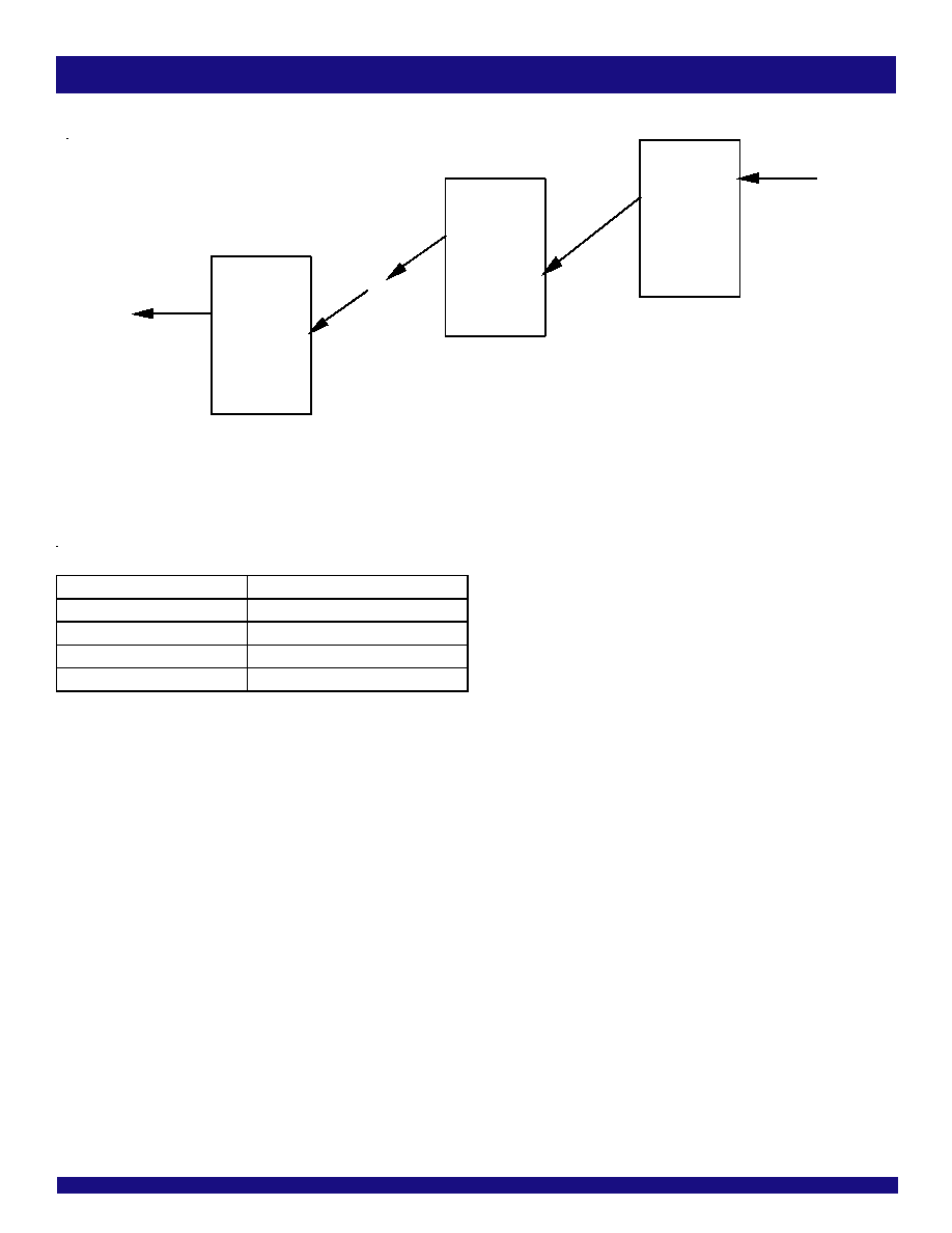
2. Time Delay Considerations
Once cascading has taken place, time delays may become critical in high
performance systems. Our main interest here is focused on "propagation
delays", i.e. calculating the time required for an input signal to propagate
through several cascaded devices up to a specific output in another device
within the cascaded system.
Propagation Delay
The propagation delay for two devices between the input and output of
interest (input to output delay) is done as follows:
1. Calculate delay between the input and C
16
in the first device.
2. Calculate delay between C
0
and the output in the second device.
3. Add both results.
The following table is an example on how to build a propagation delay
table for all inputs in a 32-bit IDT7381 cascaded system.
Propagation delay calculations can be extended to n�cascaded devices
as the sum of the delays in all devices between the input and output of interest.
That is:
(Input)
1
(C16)
1
= t
1
...
(C
0
)
i
(C
16
)
i
= t
i
(C
0
)
i + 1
(C
16
)
i + 1
= t
i + 1
...
(C
0
)
n
(Output)
n
= t
n
Where the subscript i denotes the device number and the arrow (
)
represents the delay in between. Notice that i + 1 is the immediate upper
device from device i. Adding the delays t
i
we get:
Propagation delay = t
1
+ t
2
+ ... + t
i
+ t
i + 1
+ ... + t
n
Total Delay
As seen from Figure 8, the propagation delay is within the IDT7381
devices only. A complete analysis should also include the delay associated
with the transmission line Li (which depends on the line length and its
impedance). This line delay should then be added to the propagation delay
to obtain the total delay for the cascaded system:
Total delay = Propagation delay + Transmission line delay
12
COMMERCIAL TEMPERATURE RANGE
IDT7381
16-BIT CASCADABLE ALU
Figure 1. Cascading Two IDT7381s to 32 Bits
Figure 3. Cascading Three IDT7381s to 48 Bits Wide
with a Carry-lookahead Generator
Figure 2. Cascading Three IDT7381s to 48 Bits Wide
without a Carry-lookahead Generator
G
P
C
16
OVF
Z
Z
Z
C
16
C
0
C
0
C
IN
A
16 - 31
B
16 - 31
A
0 - 15
B
0 - 15
R S
0 - 1
C lk, I
0 - 2
, EN A, EN B
EN F, FTF, FTAB
ID T73 8 1
ID T73 8 1
M S D
LS D
11
F
16 - 3 1
F
0 - 15
Z
C
16
C
0
A
0 - 15
B
0 - 15
ID T 7381
LS D
F
0 - 15
C IN
C lk, I
0 - 2
,
EN A, EN B
EN F, FTF,
FTA B
11
P
C
16
OVF
Z
Z
C
0
A
32 - 47
B
32 - 47
ID T7 381
M SD
F
32 - 4 7
Z
C
16
C
0
A
16 - 31
B
16 - 31
ID T 7381
F
16 - 3 1
G
R S
0 - 1
Z
C
0
A
0 - 15
B
0 - 15
ID T7 381
LS D
F
0 - 15
CIN
Clk, I
0 - 2
,
ENA, ENB
ENF, FTF,
FTA B
11
P
C
16
OVF
Z
Z
C
0
A
32 - 47
B
32 - 47
ID T 738 1
M S D
F
32 - 4 7
Z
C
0
A
16 - 31
B
16 - 31
ID T 738 1
F
16 - 31
G
RS
0 - 1
P
G
P
G
FC T1 82/A Lo oka h ead G ene rator
Cn
G
0
G
1
P
0
P
1
C n+x
C n+y

13
IDT7381
16-BIT CASCADABLE ALU
COMMERCIAL TEMPERATURE RANGE
Figure 4. 32-Bit Configuration for FTAB = 0, FTF = 0
Figure 5. 32-Bit Configuration for FTAB = 0, FTF = 1
A
16 - 31
B
16 - 31
A M ux
R M ux
B M ux
S M ux
16-Bit ALU
C
0
M SD
F M ux
16
16
16
F
16 - 3 1
CLK
A
0 - 15
B
0 - 15
A M ux
R M ux
B M ux
S M ux
16-Bit ALU
C
16
LSD
F M ux
16
16
16
F
0 - 15
B Reg
A Reg
B Reg
A Reg
F Reg
F Reg
A
16 - 31
B
16 - 31
A M ux
R M ux
B M ux
S M ux
16-Bit ALU
C
0
M SD
F M ux
16
16
16
F
16 - 3 1
CLK
A
0 - 15
B
0 - 15
A M ux
R M ux
B M ux
S M ux
16-Bit ALU
C
16
LSD
F M ux
16
16
16
F
0 - 15
B Reg
A Reg
B Reg
A R eg
14
COMMERCIAL TEMPERATURE RANGE
IDT7381
16-BIT CASCADABLE ALU
Figure 6. 32-Bit Configuration for FTAB = 1, FTF = 0
Figure 7. 32-Bit Configuration for FTAB = 1, FTF = 1
A
16 - 31
B
16 - 31
A M ux
R M ux
B M ux
S M ux
16-Bit ALU
C
0
M SD
F Reg
F M ux
16
16
16
F
16 - 3 1
CLK
A
0 - 15
B
0 - 15
A M ux
R M ux
B M ux
S M ux
16-Bit ALU
C
16
LSD
F Reg
F M ux
16
16
16
F
0 - 15
A
16 - 31
B
16 - 31
A M ux
R M ux
B M ux
S M ux
16-Bit ALU
C
0
M SD
F M ux
16
16
16
F
16 - 3 1
A
0 - 15
B
0 - 15
A M ux
R M ux
B M ux
S M ux
16-Bit ALU
C
16
LSD
F M ux
16
16
16
F
0 - 15
15
IDT7381
16-BIT CASCADABLE ALU
COMMERCIAL TEMPERATURE RANGE
Figure 8. Propagation Delay = t1 + t2 + . . . + tn N-Cascaded Devices
OU TPU T
IN PU T
D
0
D
1
D
n
L
1
L
2
I
n
-- t
n
--
-- t
2
--
-- t
1
--
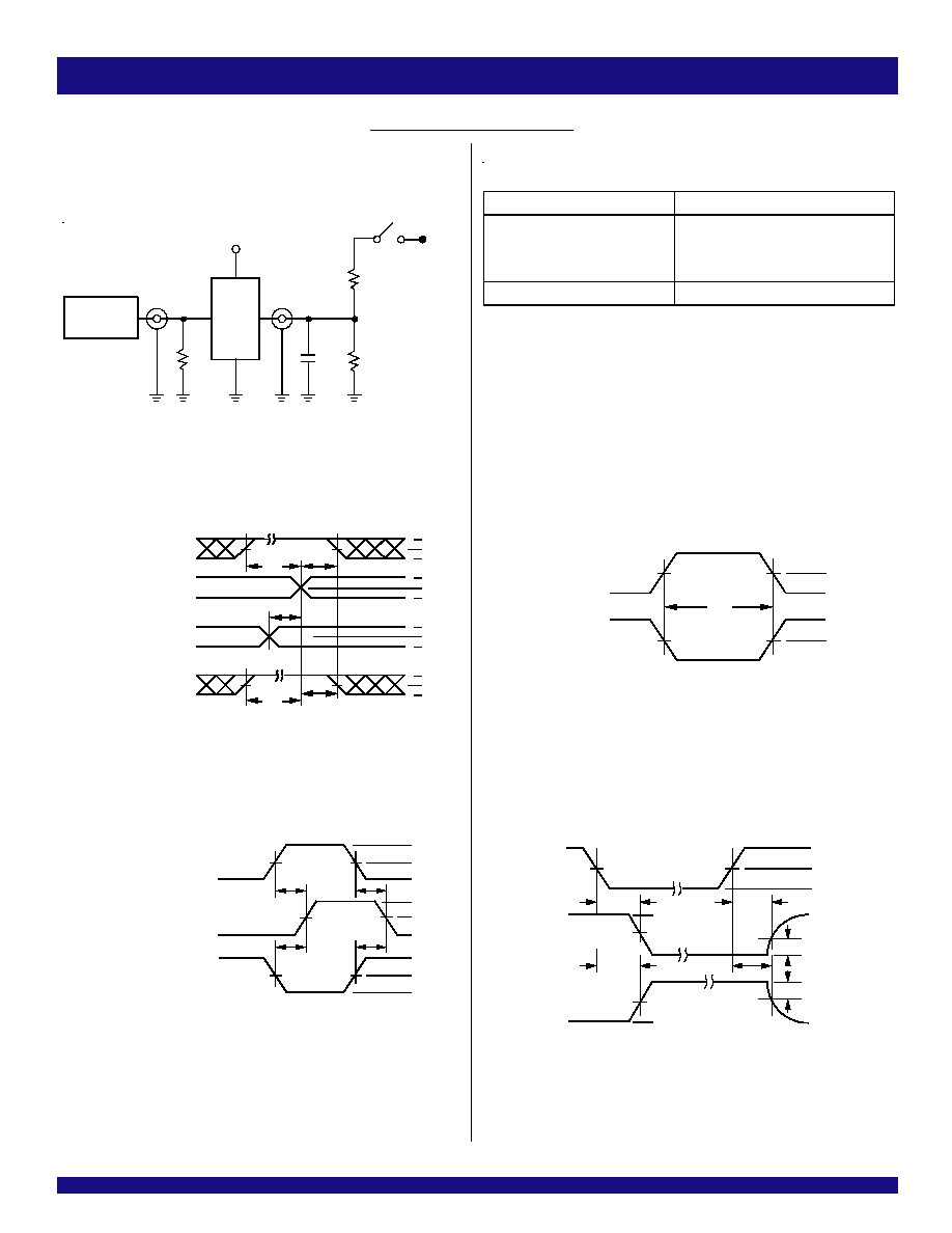
AC TEST CONDITIONS
Input Rise levels
GND to 3V
Input Rise/Fall Times
3ns
Input Timing Reference Levels
1.5V
Output Reference Levels
1.5V
Output Load
Figure 1
16
COMMERCIAL TEMPERATURE RANGE
IDT7381
16-BIT CASCADABLE ALU
Pulse
Generator
R
T
D.U.T.
V
CC
V
IN
C
L
V
OU T
50pF
500
500
7.0V
3V
1.5V
0V
3V
1.5V
0V
3V
1.5V
0V
3V
1.5V
0V
DATA
INPUT
TIMING
INPUT
ASYNCHRONOUS CONTROL
PRESET
CLEAR
ETC.
SYNCHRONOUS CONTROL
t
SU
t
H
t
REM
t
SU
t
H
PRESET
CLEAR
CLOCK ENABLE
ETC.
HIGH-LOW-HIGH
PULSE
LOW -HIGH-LOW
PULSE
t
W
1.5V
1.5V
SAME PHA SE
INPUT TRANSITION
3V
1.5V
0V
1.5V
V
OH
t
PLH
OUTPUT
OPPOS ITE P HASE
INPUT TRANSITION
3V
1.5V
0V
t
PLH
t
PH L
t
PH L
V
OL
CONTROL
INPUT
3V
1.5V
0V
3.5V
0V
OUTPUT
NORMALLY
LOW
OUTPUT
NORMALLY
HIGH
SW ITCH
CLOSE D
SWITCH
OPEN
V
O L
0.3V
0.3V
t
PLZ
t
PZL
t
PZH
t
PHZ
3.5V
0V
1.5V
1.5V
ENABLE
DISABLE
V
OH
TEST WAVEFORMS
PROPAGATION DELAY
TEST CIRCUITS FOR ALL OUTPUTS
ENABLE AND DISABLE TIMES
SET-UP, HOLD, AND RELEASE TIMES
PULSE WIDTH
NOTES:
1. Diagram shown for input Control Enable-LOW and input Control Disable-HIGH
2. Pulse Generator for All Pulses: Rate
1.0MHz; t
F
2.5ns; t
R
2.5ns
SWITCH POSITION
Test
Switch
Open Drain
Disable Low
Closed
Enable Low
All Other Tests
Open
DEFINITIONS:
C
L
=
Load capacitance: includes jig and probe capacitance.
R
T
=
Termination resistance: should be equal to Z
OUT
of the Pulse
Generator.
17
IDT7381
16-BIT CASCADABLE ALU
COMMERCIAL TEMPERATURE RANGE
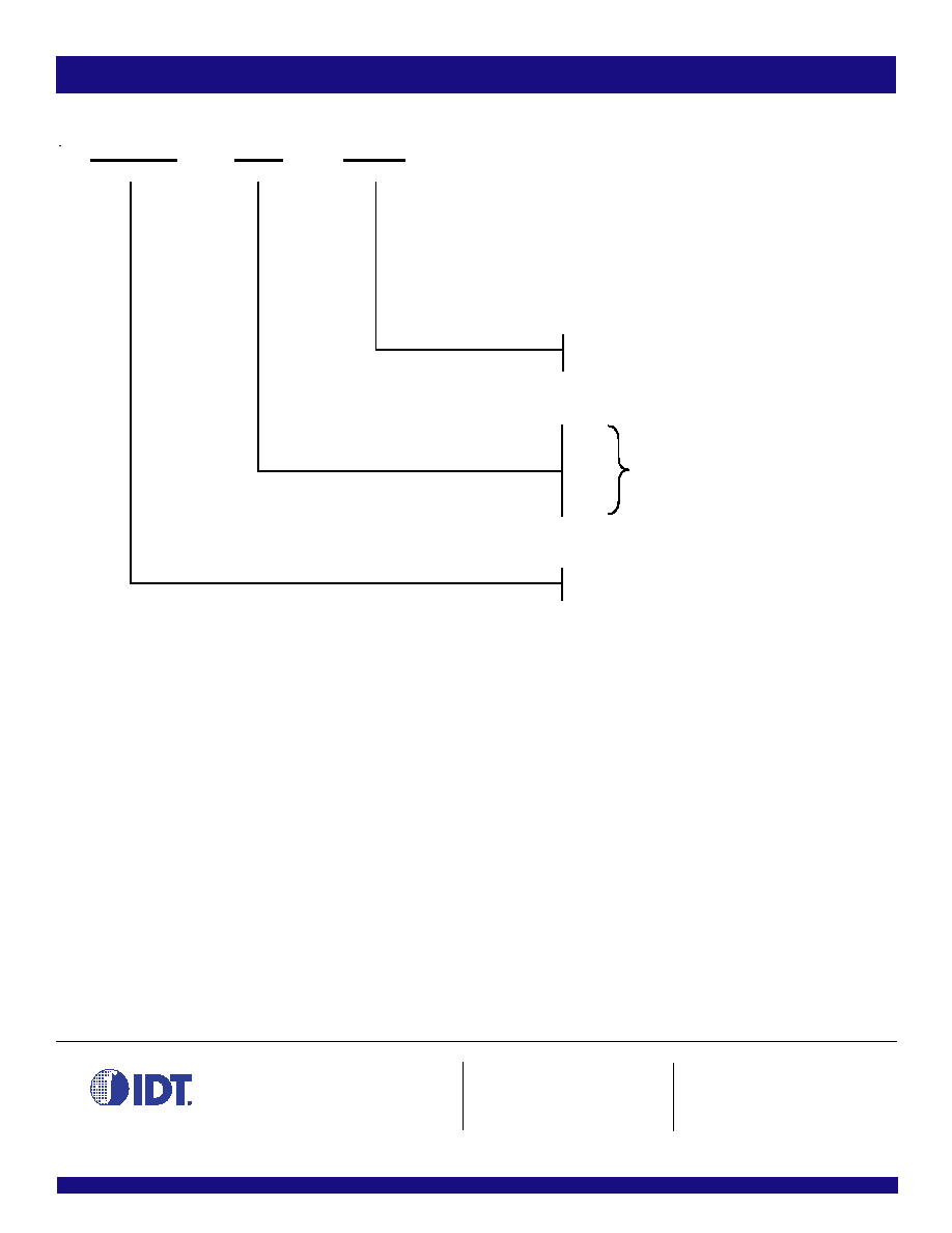
ORDERING INFORMATION
25
30
40
55
ID T
XXXX
D evice Type
XX
Speed
X
Package
J
7381L
Plastic Leaded C hip C arrier (J68-1)
Speed Grade
16-Bit ALU
CORPORATE HEADQUARTERS
for SALES:
for Tech Support:
2975 Stender Way
800-345-7015 or 408-727-6116
logichelp@idt.com
Santa Clara, CA 95054
fax: 408-492-8674
(408) 654-6459
www.idt.com