Integrated Device Technology, Inc.
FAST CMOS
OCTAL REGISTERED
TRANSCEIVERS
IDT29FCT52AT/BT/CT/DT
IDT29FCT2052AT/BT/CT
IDT29FCT53AT/BT/CT
1
The IDT logo is a registered trademark of Integrated Device Technology, Inc.
FEATURES:
∑ Common features:
≠
Low input and output leakage
1
µ
A (max.)
≠
CMOS power levels
≠
True TTL input and output compatibility
≠ V
OH
= 3.3V (typ.)
≠ V
OL
= 0.3V (typ.)
≠
Meets or exceeds JEDEC standard 18 specifications
≠
Product available in Radiation Tolerant and Radiation
Enhanced versions
≠
Military product compliant to MIL-STD-883, Class B
and DESC listed (dual marked)
≠
Available in DIP, SOIC, SSOP, QSOP, CERPACK
and LCC packages
∑ Features for 29FCT52/29FCT53T:
≠
A, B, C and D speed grades
≠
High drive outputs (-15mA I
OH
, 64mA I
OL
)
≠
Power off disable outputs permit "live insertion"
∑ Features for 29FCT2052T:
≠
A, B and C speed grades
≠
Resistor outputs
(-15mA I
OH
, 12mA I
OL
Com.)
(-12mA I
OH
, 12mA I
OL
Mil.)
≠
Reduced system switching noise
DESCRIPTION:
The IDT29FCT52AT/BT/CT/DT and IDT29FCT53AT/BT/
CT are 8-bit registered transceivers built using an advanced
dual metal CMOS technology. Two 8-bit back-to-back regis-
ters store data flowing in both directions between two bidirec-
tional buses. Separate clock, clock enable and 3-state output
enable signals are provided for each register. Both A outputs
and B outputs are guaranteed to sink 64mA.
The IDT29FCT52AT/BT/CT/DT and IDT29FCT2052AT/BT/
CT are non-inverting options of the IDT29FCT53AT/BT/CT.
The IDT29FCT2052AT/BT/CT has balanced drive outputs
with current limiting resistors. This offers low ground bounce,
minimal undershoot and controlled output fall times-reducing
the need for external series terminating resistors. The
IDT29FCT2052T part is a plug-in replacement for
IDT29FCT52T part.
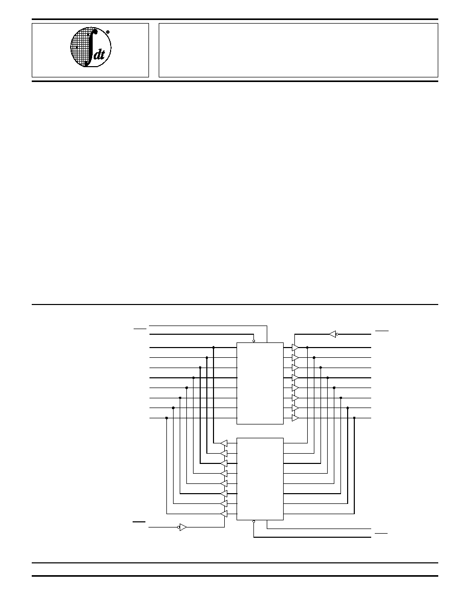
FUNCTIONAL BLOCK DIAGRAM
(1)
CPA
A
0
2629 drw 01
CEA
A
1
A
2
A
3
A
4
A
5
A
6
A
7
B
0
OEB
B
1
B
2
B
3
B
4
B
5
B
6
B
7
Q
0
Q
1
Q
2
Q
3
Q
4
Q
5
Q
6
Q
7
D
0
D
1
D
2
D
3
D
4
D
5
D
6
D
7
CE CP
A
Reg.
D
0
D
1
D
2
D
3
D
4
D
5
D
6
D
7
Q
0
Q
1
Q
2
Q
3
Q
4
Q
5
Q
6
Q
7
CE CP
B
Reg.
OEA
CPB
CEB
NOTE:
1. IDT29FCT52T/IDT29FCT2052T function is shown. IDT29FCT53T is
the inverting option.
MILITARY AND COMMERCIAL TEMPERATURE RANGES
JUNE 1995
©
1995 Integrated Device Technology, Inc.
6.1
DSC-4224/5
IDT29FCT52AT/BT/CT/DT, IDT29FCT/2052AT/BT/CT, IDT29FCT53AT/BT/CT
FAST CMOS OCTAL REGISTERED TRANSCEIVERS
MILITARY AND COMMERCIAL TEMPERATURE RANGES
6.1
2
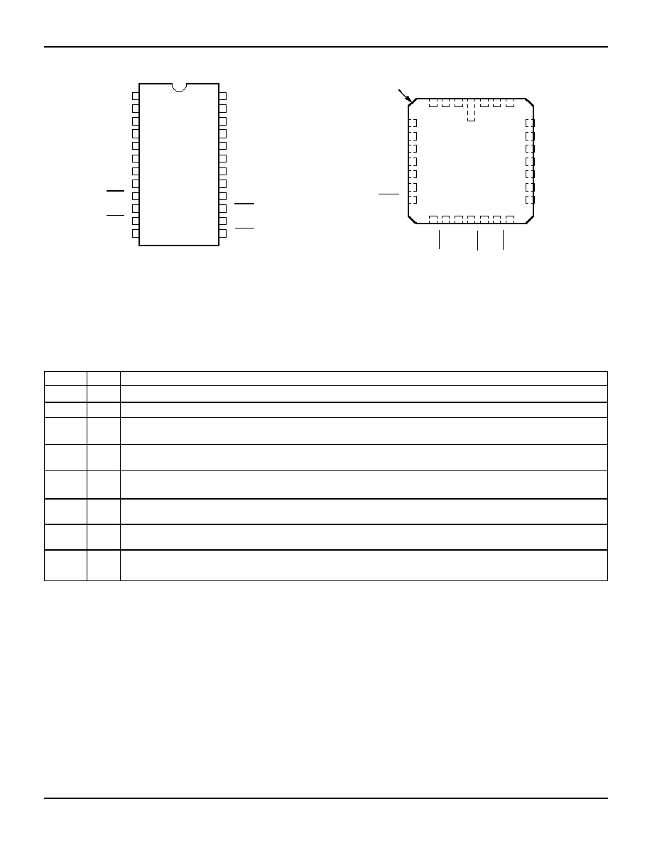
PIN CONFIGURATIONS
5
6
7
8
9
10
11
12
GND
1
2
3
4
24
23
22
21
20
19
18
17
Vcc
16
15
14
13
P24-1
D24-1
SO24-2
SO24-7*
SO24-8*
&
E24-1
A
6
A
5
A
4
A
3
A
2
CEB
CEA
CPB
CPA
OEA
A
1
A
0
A
7
B
6
B
5
B
4
B
3
B
2
B
1
B
B
7
0
OEB
2629 drw 02
5
6
7
8
9
10
11
L28-1
25
24
23
22
21
20
19
12 13 14 15 16 17 18
4
3
2
1
28 27 26
INDEX
2629 drw 03
B
3
B
2
B
1
B
0
A
5
A
4
A
3
A
2
A
1
A
0
OEB
NC
NC
GND
CEB
CEA
CPB
CPA
OEA
NC
B
4
B
5
Vcc
A
6
A
7
B
6
NC
B
7
DIP/SOIC/SSOP/QSOP/CERPACK
TOP VIEW
LCC
TOP VIEW
* For 29FCT52/29FCT2052AT/BT/CT only
PIN DESCRIPTION
Name
I/O
Description
A
0-7
I/O
Eight bidirectional lines carrying the A Register inputs or B Register outputs.
B
0-7
I/O
Eight bidirectional lines carrying the B Register inputs or A Register outputs.
CPA
I
Clock for the A Register. When
CEA
is LOW, data is entered into the A Register on the LOW-to-HIGH transition of
the CPA signal.
CEA
I
Clock Enable for the A Register. When
CEA
is LOW, data is entered into the A Register on the LOW-to-HIGH transition
of the CPA signal. When
CEA
is HIGH, the A Register holds its contents, regardless of CPA signal transitions.
OEB
I
Output Enable for the A Register. When
OEB
is LOW, the A Register outputs are enabled onto the B
0-7
lines. When
OEB
is HIGH, the B
0-7
outputs are in the high-impedance state.
CPB
I
Clock for the B Register. When
CEB
is LOW, data is entered into the B Register on the LOW-to-HIGH transition of
the CPB signal.
CEB
I
Clock Enable for the B Register. When
CEB
is LOW, data is entered into the B Register on the LOW-to-HIGH transition
of the CPB signal. When
CEB
is HIGH, the B Register holds its contents, regardless of CPB signal transitions.
OEA
I
Output Enable for the B Register. When
OEA
is LOW, the B Register outputs are enabled onto the A
0-7
lines. When
OEA
is HIGH, the A
0-7
outputs are in the high-impedance state.
2629 tbl 01
IDT29FCT52AT/BT/CT/DT, IDT29FCT/2052AT/BT/CT, IDT29FCT53AT/BT/CT
FAST CMOS OCTAL REGISTERED TRANSCEIVERS
MILITARY AND COMMERCIAL TEMPERATURE RANGES
6.1
3
NOTE:
1. H = HIGH Voltage Level
L = LOW Voltage Level
X = Don't Care
NC = No Change
= LOW-to-HIGH Transition
REGISTER FUNCTION TABLE
(1)
(Applies to A or B Register)
Inputs
Internal
D
CP
CE
CE
Q
Function
X
X
H
NC
Hold Data
L
L
L
Load Data
H
L
H
2629 tbl 02
OUTPUT CONTROL
(1)
Internal
Y-Outputs
OE
OE
Q
52/2052
53
Function
H
X
Z
Z
Disable Outputs
L
L
L
H
Enable Outputs
L
H
H
L
NOTE:
2629 tbl 03
1. H = HIGH Voltage Level
L = LOW Voltage Level
X = Don't Care
Z = High Impedance
CAPACITANCE
(T
A
= +25
∞
C, f = 1.0MHz)
ABSOLUTE MAXIMUM RATINGS
(1)
2529 lnk 04
Symbol
Parameter
(1)
Conditions
Typ.
Max. Unit
C
IN
Input
Capacitance
V
IN
= 0V
6
10
pF
C
OUT
Output
Capacitance
V
OUT
= 0V
8
12
pF
NOTE:
1. This parameter is measured at characterization but not tested.
2640 lnk 05
Symbol
Rating
Commercial
Military
Unit
V
TERM(2)
Terminal Voltage
with Respect to
GND
≠0.5 to +7.0
≠0.5 to +7.0
V
V
TERM(3)
Terminal Voltage
with Respect to
GND
≠0.5 to
V
CC
+0.5
≠0.5 to
V
CC
+0.5
V
T
A
Operating
Temperature
0 to +70
≠55 to +125
∞
C
T
BIAS
Temperature
Under Bias
≠55 to +125
≠65 to +135
∞
C
T
STG
Storage
Temperature
≠55 to +125
≠65 to +150
∞
C
P
T
Power Dissipation
0.5
0.5
W
I
OUT
DC Output
Current
≠60 to +120 ≠60 to +120 mA
NOTES:
1. Stresses greater than those listed under ABSOLUTE MAXIMUM RAT-
INGS may cause permanent damage to the device. This is a stress rating
only and functional operation of the device at these or any other condi-
tions above those indicated in the operational sections of this specifica-
tion is not implied. Exposure to absolute maximum rating conditions for
extended periods may affect reliability. No terminal voltage may exceed
V
CC
by +0.5V unless otherwise noted.
2. Input and V
CC
terminals only.
3. Outputs and I/O terminals only.
IDT29FCT52AT/BT/CT/DT, IDT29FCT/2052AT/BT/CT, IDT29FCT53AT/BT/CT
FAST CMOS OCTAL REGISTERED TRANSCEIVERS
MILITARY AND COMMERCIAL TEMPERATURE RANGES
6.1
4
DC ELECTRICAL CHARACTERISTICS OVER OPERATING RANGE
Following Conditions Apply Unless Otherwise Specified:
Commercial: T
A
= 0
∞
C to +70
∞
C, V
CC
= 5.0V
±
5%; Military: T
A
= ≠55
∞
C to +125
∞
C, V
CC
= 5.0V
±
10%
Symbol
Parameter
Test Conditions
(1)
Min.
Typ.
(2)
Max.
Unit
V
IH
Input HIGH Level
Guaranteed Logic HIGH Level
2.0
--
--
V
V
IL
Input LOW Level
Guaranteed Logic LOW Level
--
--
0.8
V
I
I H
Input HIGH Current
(4)
V
CC
= Max.
V
I
= 2.7V
--
--
±
1
µ
A
I
I L
Input LOW Current
(4)
V
I
= 0.5V
--
--
±
1
I
OZH
High Impedance Output Current
V
CC
= Max.
V
O
= 2.7V
--
--
±
1
µ
A
I
OZL
(3-State Output pins)
(4)
V
O
= 0.5V
--
--
±
1
I
I
Input HIGH Current
(4)
V
CC
= Max., V
I
= V
CC
(Max.)
--
--
±
1
µ
A
V
IK
Clamp Diode Voltage
V
CC
= Min., I
IN
= ≠18mA
--
≠0.7
≠1.2
V
V
H
Input Hysteresis
--
--
200
--
mV
I
CC
Quiescent Power Supply Current
V
CC
= Max., V
IN
= GND or V
CC
--
0.01
1
mA
OUTPUT DRIVE CHARACTERISTICS FOR 29FCT52T/29FCT53T
Symbol
Parameter
Test Conditions
(1)
Min.
Typ.
(2)
Max.
Unit
V
OH
Output HIGH Voltage
V
CC
= Min.
V
IN
= V
IH
or V
IL
I
OH
= ≠6mA MIL.
I
OH
= ≠8mA COM'L.
2.4
3.3
--
V
I
OH
= ≠12mA MIL.
I
OH
= ≠15mA COM'L.
2.0
3.0
--
V
V
OL
Output LOW Voltage
V
CC
= Min.
V
IN
= V
IH
or V
IL
I
OL
= 48mA MIL.
I
OL
= 64mA COM'L.
--
0.3
0.55
V
I
OS
Short Circuit Current
V
CC
= Max., V
O
= GND
(3)
≠60
≠120
≠225
mA
I
OFF
Input/Output Power Off Leakage
(5)
V
CC
= 0V, V
IN
or V
O
4.5V
--
--
±
1
µ
A
OUTPUT DRIVE CHARACTERISTICS FOR 29FCT2052T
Symbol
Parameter
Test Conditions
(1)
Min.
Typ.
(2)
Max.
Unit
I
ODL
Output LOW Current
V
CC
= 5V, V
IN
= V
IH
or
V
IL,
V
OUT
= 1.5V
(3)
16
48
--
mA
I
ODH
Output HIGH Current
V
CC
= 5V, V
IN
= V
IH
or V
IL,
V
OUT
= 1.5V
(3)
≠16
≠48
--
mA
V
OH
Output HIGH Voltage
V
CC
= Min.
V
IN
= V
IH
or
V
IL
I
OH
= ≠12mA MIL.
I
OH
= ≠15mA COM'L.
2.4
3.3
--
V
V
OL
Output LOW Voltage
V
CC
= Min.
V
IN
= V
IH
or V
IL
I
OL
= 12mA
--
0.3
0.50
V
NOTES:
1. For conditions shown as Max. or Min., use appropriate value specified under Electrical Characteristics for the applicable device type.
2. Typical values are at Vcc = 5.0V, +25
∞
C ambient.
3. Not more than one output should be shorted at one time. Duration of the short circuit test should not exceed one second.
4. The test limit for this parameter is
±
5
µ
A at T
A
= ≠55
∞
C.
5. This parameter is guaranteed but not tested.
2629 tbl 06
2629 tbl 07
2629 tbl 08
IDT29FCT52AT/BT/CT/DT, IDT29FCT/2052AT/BT/CT, IDT29FCT53AT/BT/CT
FAST CMOS OCTAL REGISTERED TRANSCEIVERS
MILITARY AND COMMERCIAL TEMPERATURE RANGES
6.1
5
POWER SUPPLY CHARACTERISTICS
Symbol
Parameter
Test Conditions
(1)
Min.
Typ.
(2)
Max.
Unit
I
CC
Quiescent Power Supply Current
TTL Inputs HIGH
V
CC
= Max.
V
IN
= 3.4V
(3)
--
0.5
2.0
mA
I
CCD
Dynamic Power Supply Current
(4)
V
CC
= Max.
Outputs Open
OE
A
or
OE
B
= GND
V
IN
= V
CC
V
IN
= GND
FCTxxxT
--
0.15
0.25
mA/
MHz
One Input Toggling
50% Duty Cycle
FCT2xxxT
--
0.06
0.12
I
C
Total Power Supply Current
(6)
V
CC
= Max.
Outputs Open
V
IN
= V
CC
V
IN
= GND
FCTxxxT
--
1.5
3.5
mA
f
CP
= 10MHz
50% Duty Cycle
FCT2xxxT
--
0.6
2.2
OE
A
or
OE
B
= GND
V
IN
= 3.4V
FCTxxxT
--
2.0
5.5
One Bit Toggling
at fi = 5MHz
50% Duty Cycle
V
IN
= GND FCT2xxxT
1.1
4.2
V
CC
= Max.
Outputs Open
V
IN
= V
CC
V
IN
= GND
FCTxxxT
--
3.8
7.3
(5)
f
CP
= 10MHz
50% Duty Cycle
FCT2xxxT
--
1.5
4.0
(5)
OE
A
or
OE
B
= GND
V
IN
= 3.4V
FCTxxxT
--
6.0
16.3
(5)
Eight Bits Toggling
at fi = 2.5MHz
50% Duty Cycle
V
IN
= GND FCT2xxxT
--
3.8
13.0
(
5)
NOTES:
1. For conditions shown as Max. or Min., use appropriate value specified under Electrical Characteristics for the applicable device type.
2. Typical values are at V
CC
= 5.0V, +25
∞
C ambient.
3. Per TTL driven input (V
IN
= 3.4V). All other inputs at V
CC
or GND.
4. This parameter is not directly testable, but is derived for use in Total Power Supply Calculations.
5. Values for these conditions are examples of the I
CC
formula. These limits are guaranteed but not tested.
6. I
C
= I
QUIESCENT
+ I
INPUTS
+ I
DYNAMIC
I
C
= I
CC
+
I
CC
D
H
N
T
+ I
CCD
(f
CP/
2 + f
i
N
i
)
I
CC
= Quiescent Current
I
CC
= Power Supply Current for a TTL High Input (V
IN
= 3.4V)
D
H
= Duty Cycle for TTL Inputs High
N
T
= Number of TTL Inputs at D
H
I
CCD
= Dynamic Current Caused by an Input Transition Pair (HLH or LHL)
f
CP
= Clock Frequency for Register Devices (Zero for Non-Register Devices)
f
i
= Input Frequency
N
i
= Number of Inputs at f
i
All currents are in milliamps and all frequencies are in megahertz.
2629 tbl 09