1
INDUSTRIAL TEMPERATURE RANGE
IDT74CBTLV16800
LOW-VOLTAGE 20-BIT BUS SWITCH WITH PRECHARGED OUTPUTS
AUGUST 2002
2002 Integrated Device Technology, Inc.
DSC-5886/5
c
INDUSTRIAL TEMPERATURE RANGE
APPLICATIONS:
∑ 3.3V High Speed Bus Switching and Bus Isolation
FEATURES:
∑ 5
A/B bi-directional switch
∑ Isolation Under Power-Off Conditions
∑ Over-voltage tolerant
∑ Latch-up performance exceeds 100mA
∑ V
CC
= 2.3V - 3.6V, normal range
∑ ESD >2000V per MIL-STD-883, Method 3015; >200V using
machine model (C = 200pF, R = 0)
∑ Available in SSOP, TSSOP, and TVSOP packages
The IDT logo is a registered trademark of Integrated Device Technology, Inc.
2
12
1A1
1A10
46
36
SW
SW
1B1
1B10
BIASV
1
1OE
48
24
2A1
2A10
35
25
SW
SW
2B1
2B10
2OE
1
13
IDT74CBTLV16800
PRELIMINARY
FUNCTIONAL BLOCK DIAGRAM
LOW-VOLTAGE 20-BIT
BUS SWITCH WITH
PRECHARGED OUTPUTS
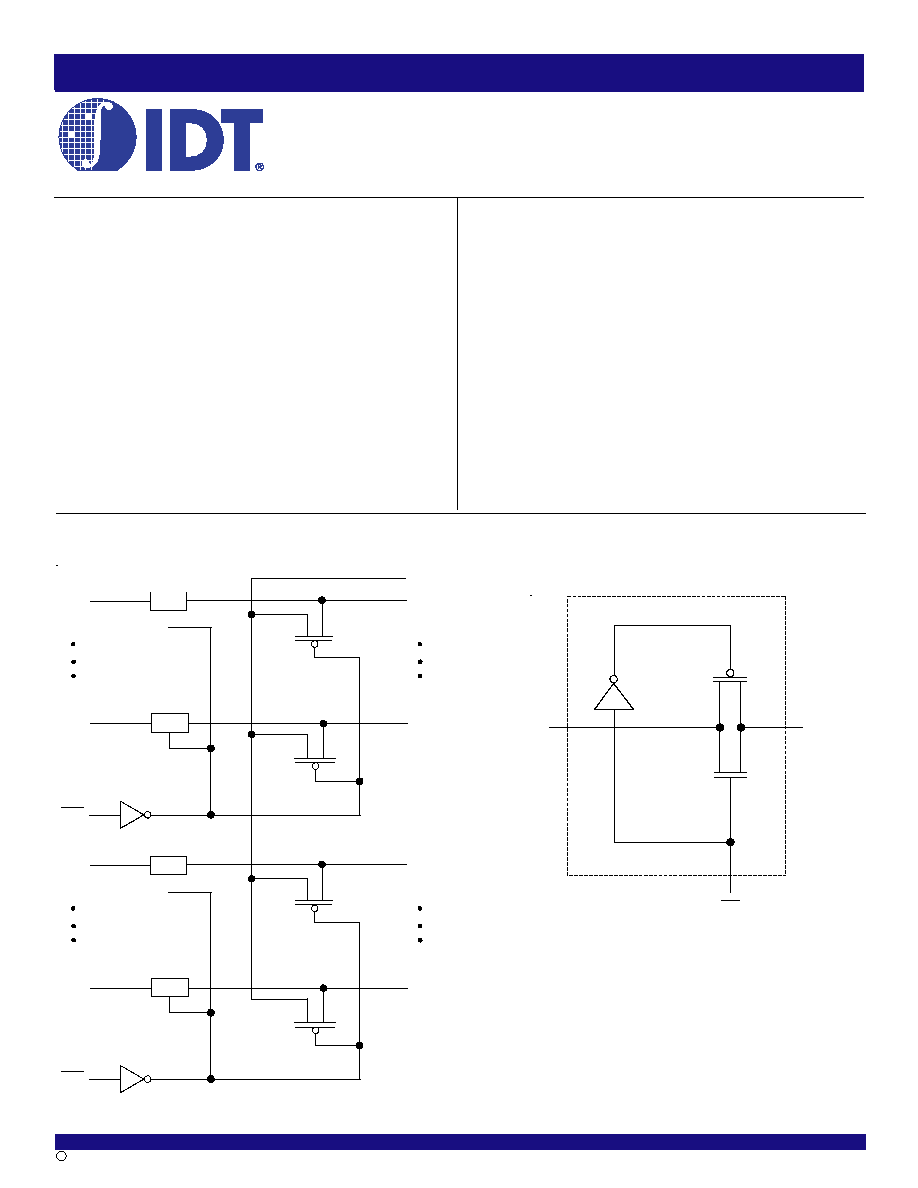
DESCRIPTION:
The CBTLV16800 provides 20-bits of high-speed bus switching with low
on-state resistance of the switch allowing connections to be made with
minimal propagation delay. The device also precharges the B port to a
user-selectable bias voltage (BIASV) to minimize live-insertion noise.
The CBTLV16800 is organized as dual 10-bit bus switches with two
different output-enable (OE) control inputs. When OE is low, the corre-
sponding 10-bit bus switch is on and port A is connected to port B. When
OE is high, the switch is open, and a high impedance state exists between
the two ports, and port B is precharged to BIASV through the equivalent
of a 10-k
resistor.
To ensure the high-impedance state during power up or power down,
OE should be tied to V
CC
through a pullup resistor; the minimum value of
the resistor is determined by the current-sinking capability of the driver.
O E
A
B
SIMPLIFIED SCHEMATIC, EACH
SWITCH
2
INDUSTRIAL TEMPERATURE RANGE
IDT74CBTLV16800
LOW-VOLTAGE 20-BIT BUS SWITCH WITH PRECHARGED OUTPUTS
ABSOLUTE MAXIMUM RATINGS
(1)
Symbol
Description
Max.
Unit
V
CC
Supply Voltage Range
≠0.5 to 4.6
V
BIASV
Bias Voltage Range, V
I
≠0.5 to 4.6
V
V
I
Input Voltage Range
≠0.5 to 4.6
V
Continuous Channel Current
128
mA
I
IK
Input Clamp Current, V
I/O
< 0
≠50
mA
T
STG
Storage Temperature Range
≠65 to +150
∞C
NOTE:
1. Stresses greater than those listed under ABSOLUTE MAXIMUM RATINGS may cause
permanent damage to the device. This is a stress rating only and functional operation
of the device at these or any other conditions above those indicated in the operational
sections of this specification is not implied. Exposure to absolute maximum rating
conditions for extended periods may affect reliability.
NOTE:
1. H = HIGH Voltage Level
L = LOW Voltage Level
Z = High-Impedance
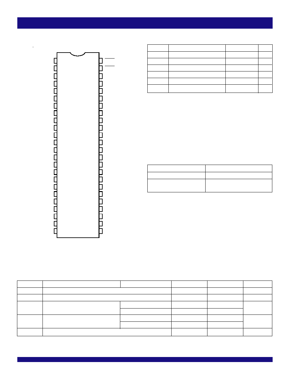
PIN CONFIGURATION
Input OE
Inputs/Outputs
L
A-Port = B-Port
H
A-Port = Z
B-Port = BIASV
FUNCTION TABLE
(EACH 10-BIT BUS SWITCH)
(1)
OPERATING CHARACTERISTICS
(1)
Symbol
Parameter
Test Conditions
Min.
Max.
Unit
V
CC
Supply Voltage
2.3
3.6
V
BIASV
Bias Voltage
1.3
V
CC
V
V
IH
High-Level Control Input Voltage
V
CC
= 2.3V to 2.7V
1.7
--
V
V
CC
= 2.7V to 3.6V
2
--
V
IL
Low-Level Control Input Voltage
V
CC
= 2.3V to 2.7V
--
0.7
V
V
CC
= 2.7V to 3.6V
--
0.8
T
A
Operating Free-Air Temperature
≠40
+85
∞C
NOTE:
1. All unused control inputs of the device must be held at V
CC
or GND to ensure proper device operation.
SSOP/ TSSOP/ TVSOP
TOP VIEW
48
47
46
45
44
43
42
41
40
39
38
37
36
35
34
33
32
31
30
29
28
27
26
25
1OE
2OE
1
2
3
4
5
6
7
8
9
10
11
12
13
14
15
16
17
18
19
20
21
22
23
24
BIASV
1
A
1
GND
1
A
2
1
A
3
1
A
4
V
CC
1
A
5
1
A
6
1
A
7
1
A
8
2
A
1
2
A
2
2
A
3
2
A
4
GND
2
A
5
2
A
6
2
A
7
2
A
8
1
A
9
1
A
10
2
A
9
2
A
10
1
B
1
GND
1
B
2
1
B
3
1
B
4
1
B
5
1
B
6
1
B
7
1
B
8
2
B
1
2
B
2
2
B
3
2
B
4
GND
2
B
5
2
B
6
2
B
7
2
B
8
1
B
9
1
B
10
2
B
9
2
B
10
3
INDUSTRIAL TEMPERATURE RANGE
IDT74CBTLV16800
LOW-VOLTAGE 20-BIT BUS SWITCH WITH PRECHARGED OUTPUTS
DC ELECTRICAL CHARACTERISTICS OVER OPERATING RANGE
Following Conditions Apply Unless Otherwise Specified:
Operating Condition: T
A
= ≠40∞C to +85∞C
NOTES:
1. The increase in supply current is attributable to each input that is at the specified voltage level rather than V
CC
or GND.
2. This is measured by the voltage drop between the A and B terminals at the indicated current through the switch. On-state resistance is determined by the lower of the voltages
of the two (A or B) terminals.
Symbol
Parameter
Test Conditions
Min.
Typ.
Max.
Unit
V
IK
Control Inputs, Data I/O
V
CC
= 3V, I
I
= ≠18mA
--
--
≠1.2
V
I
I
Control Inputs
V
CC
= 3.6V, V
I
= V
CC
or GND
--
--
±1
µA
I
OZ
Data I/O
V
CC
= 3.6V, V
O
= 0V or 3.6V switch disabled
--
--
5
µA
I
OFF
A Port
V
CC
= 0V, V
I
or V
O
= 0V or 3.6V
--
--
10
µA
I
O
V
CC
= 3V, BIASV = 2.4V, V
O
= 0, OE = V
CC
| 0.25 |
--
--
mA
I
CC
V
CC
= 3.6V, I
O
= 0, V
I
= V
CC
or GND
--
--
10
µA
I
CC(1)
Control Inputs
V
CC
= 3.6V, one input at 3V, other inputs at V
CC
or GND
--
--
300
µA
C
I
Control Inputs
V
I
= 3V or 0
--
4
--
pF
C
IO(OFF)
V
O
= 3V or 0, switch off, BIASV = open, OE = V
CC
--
6.5
--
pF
V
CC
= 2.3V
V
I
= 0
I
I
= 64mA
--
5
9
Typ. at V
CC
= 2.5V
I
I
= 24mA
--
5
9
R
ON
V
I
= 1.7V
I
I
= 15mA
--
25
35
V
I
= 0
I
I
= 64mA
--
5
7
V
CC
= 3V
I
I
= 24mA
--
5
7
V
I
= 2.4V
I
I
= 15mA
--
10
15
V
CC
= 2.5V ± 0.2V
V
CC
= 3.3V ± 0.3V
Symbol
Parameter
Min.
Max.
Min.
Max.
Unit
t
PD(1)
Propagation Delay
--
0.15
--
0.25
ns
A to B or B to A
t
PZH
BIASV = GND
2.9
7.7
2.2
5.5
ns
OE to A or B
t
PZL
BIASV = 3V
2.8
6.4
2.1
5.3
ns
OE to A or B
t
PHZ
BIASV = GND
1.4
6.8
2.6
7.6
ns
OE to A or B
t
PLZ
BIASV = 3V
1.3
4.2
1.5
5.1
ns
OE to A or B
NOTE:
1. The propagation delay is the calculated RC time constant of the typical on-state resistance of the switch and the specified load capacitance when driven by an ideal voltage source
(zero output impededance).
SWITCHING CHARACTERISTICS
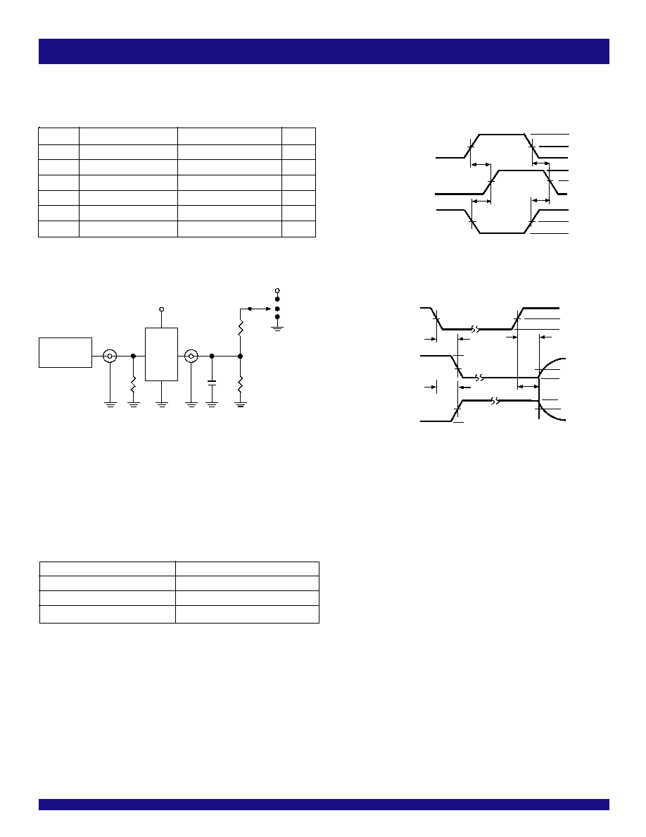
4
INDUSTRIAL TEMPERATURE RANGE
IDT74CBTLV16800
LOW-VOLTAGE 20-BIT BUS SWITCH WITH PRECHARGED OUTPUTS
O pen
V
LOAD
GND
V
C C
Pulse
Generator
D.U.T.
500
500
C
L
R
T
V
IN
V
OUT
(1, 2)
SAM E PHAS E
INPUT TRANSITIO N
O PPOSITE PHASE
INPUT TRANSITION
0V
0V
V
OH
V
O L
t
P LH
t
PH L
t
PHL
t
PLH
OUTPUT
V
IH
V
T
V
T
V
IH
V
T
CONTROL
INPUT
t
PLZ
0V
OUTPUT
NORM ALLY
LO W
t
PZ H
0V
SW ITCH
CLO SED
OUTPUT
NORM ALLY
HIGH
ENABLE
DISABLE
SW ITCH
O PEN
t
PHZ
0V
V
OL +
V
LZ
V
OH
V
T
V
T
t
PZL
V
LO AD/2
V
LOA D/2
V
IH
V
T
V
OL
V
OH -
V
HZ
TEST CIRCUITS AND WAVEFORMS
Propagation Delay
Test Circuits for All Outputs
Enable and Disable Times
NOTE:
1. Diagram shown for input Control Enable-LOW and input Control Disable-HIGH.
DEFINITIONS:
C
L
= Load capacitance: includes jig and probe capacitance.
R
T
= Termination resistance: should be equal to Z
OUT
of the Pulse Generator.
NOTES:
1. Pulse Generator for All Pulses: Rate
10MHz; t
F
2.5ns; t
R
2.5ns.
2. Pulse Generator for All Pulses: Rate
10MHz; t
F
2ns; t
R
2ns.
Test
Switch
t
PLZ
/t
PZL
V
LOAD
t
PHZ
/t
PZH
GND
t
PD
Open
SWITCH POSITION
Symbol
V
CC(1)
= 3.3V±0.3V
V
CC(2)
= 2.5V±0.2V
Unit
V
LOAD
6
2 x Vcc
V
V
IH
3
Vcc
V
V
T
1.5
Vcc
/ 2
V
V
LZ
300
150
mV
V
HZ
300
150
mV
C
L
50
30
pF
TEST CONDITIONS
5
INDUSTRIAL TEMPERATURE RANGE
IDT74CBTLV16800
LOW-VOLTAGE 20-BIT BUS SWITCH WITH PRECHARGED OUTPUTS
ORDERING INFORMATION
CORPORATE HEADQUARTERS
for SALES:
for Tech Support:
2975 Stender Way
800-345-7015 or 408-727-6116
logichelp@idt.com
Santa Clara, CA 95054
fax: 408-492-8674
(408) 654-6459
www.idt.com
IDT
XX
CBTLV
XXX
XX
Package
Device Type
Temp. Range
PV
PA
PF
74
Shrink Small Outline Package
Thin Shrink Small Outline Package
Thin Very Small Outline Package
Low-Voltage 20-Bit Bus Switch with Precharged Outputs
≠40∞C to +85∞C
16800