1
IDT74FCT162344AT/CT/ET
FAST CMOS ADDRESS/CLOCK DRIVER
INDUSTRIAL TEMPERATURE RANGE
MAY 2002
IDT74FCT162344AT/CT/ET
FAST CMOS
ADDRESS/CLOCK
DRIVER
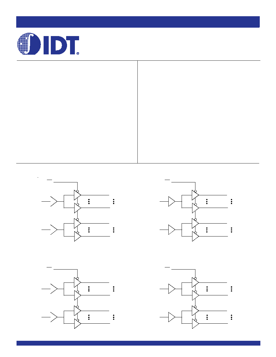
DESCRIPTION:
The FCT162344T is a 1:4 address/clock driver built using advanced dual
metal CMOS technology. This high-speed, low power device provides the
ability to fanout to memory arrays. Eight banks, each with a fanout of 4, and
3-state control provide efficient address distribution. One or more banks may
be used for clock distribution.
The FCT162344T has balanced output drive with current limiting resistors.
This offers low ground bounce, minimal undershoot and controlled output fall
times reducing the need for external series terminating resistors.
A large number of power and ground pins and TTL output swings also ensure
reduced noise levels. All inputs are designed with hysteresis for improved noise
margins.
A
1
B
11
B
14
OE
1
A
2
B
21
B
24
A
3
B
31
B
34
OE
2
A
4
B
41
B
44
A
5
B
51
B
54
OE
3
A
6
B
61
B
64
A
7
B
71
B
74
OE
4
A
8
B
81
B
84
1
8
14
2
6
9
13
28
15
21
16
20
23
27
29
36
42
34
30
41
37
56
43
49
48
44
55
51
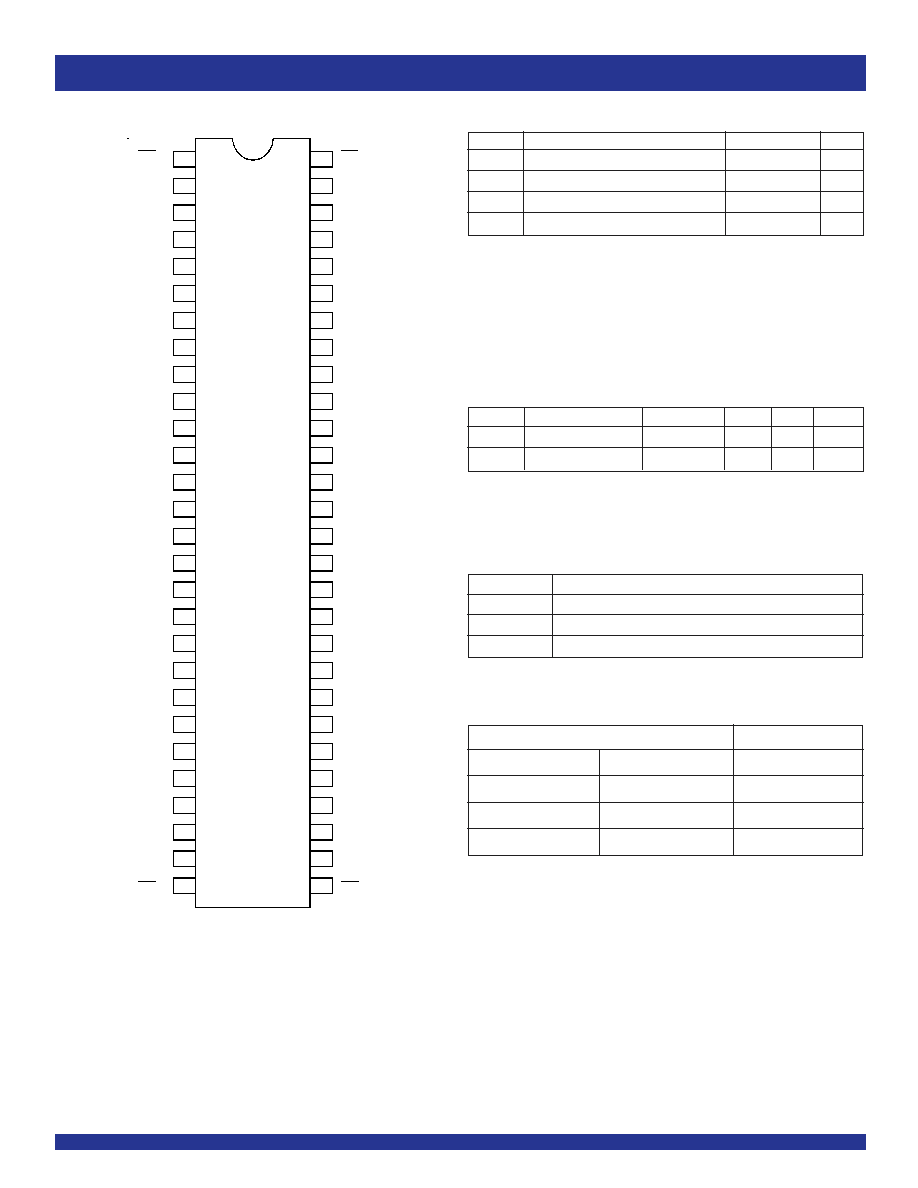
FUNCTIONAL BLOCK DIAGRAM
FEATURES:
∑ 0.5 MICRON CMOS Technology
∑ Ideal for address line driving and clock distribution
∑ 8 banks with 1:4 fanout and 3-state
∑ Typical t
SK(o)
(Output Skew) < 500ps
∑ Balanced Output Drivers (±24mA)
∑ Reduced system switching noise
∑ ESD > 2000V per MIL-STD-883, Method 3015; > 200V using
machine model (C = 200pF, R = 0)
∑ V
CC
= 5V ± 10%
∑ Low input and output leakage
1µA (max.)
∑ Available in SSOP and TSSOP packages
The IDT logo is a registered trademark of Integrated Device Technology, Inc.
© 2002 Integrated Device Technology, Inc.
DSC-3069/6
INDUSTRIAL TEMPERATURE RANGE
2
INDUSTRIAL TEMPERATURE RANGE
IDT74FCT162344AT/CT/ET
FAST CMOS ADDRESS/CLOCK DRIVER
SSOP/ TSSOP
TOP VIEW
PIN CONFIGURATION
OE1
B
11
GND
B
13
V
CC
B
22
A
2
A
3
GND
A
4
B
12
B
14
A
1
B
21
GND
B
23
B
24
B
31
B
32
B
33
V
CC
B
41
B
34
B
42
B
81
B
82
GND
B
83
B
84
V
CC
A
8
B
71
GND
B
73
B
74
A
7
B
61
B
62
GND
B
63
V
CC
B
51
B
64
B
72
A
6
A
5
B
52
OE4
39
29
30
31
32
33
34
35
36
37
38
25
26
27
28
48
47
41
42
43
44
45
46
40
1
2
3
4
5
6
7
8
9
10
12
13
14
15
16
17
18
19
20
11
21
22
23
24
B
44
GND
OE2
B
43
OE3
GND
B
53
B
54
49
56
55
50
51
52
53
54
Symbol
Description
Max
Unit
V
TERM
(2)
Terminal Voltage with Respect to GND
≠0.5 to +7
V
V
TERM
(3)
Terminal Voltage with Respect to GND
≠0.5 to V
CC
+0.5
V
T
STG
Storage Temperature
≠65 to +150
∞C
I
OUT
DC Output Current
≠60 to +120
mA
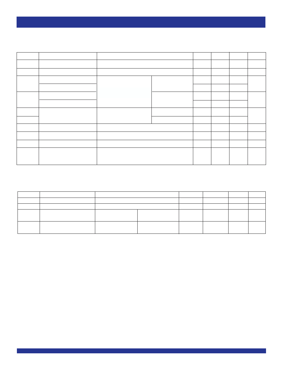
ABSOLUTE MAXIMUM RATINGS
(1)
(1)
(1)
(1)
(1)
NOTES:
1. Stresses greater than those listed under ABSOLUTE MAXIMUM RATINGS may cause
permanent damage to the device. This is a stress rating only and functional operation
of the device at these or any other conditions above those indicated in the operational
sections of this specification is not implied. Exposure to absolute maximum rating
conditions for extended periods may affect reliability.
2. All device terminals except FCT162XXX Output and I/O terminals.
3. Output and I/O terminals terminals for FCT162XXX.
Symbol
Parameter
(1)
Conditions
Typ.
Max.
Unit
C
IN
Input Capacitance
V
IN
= 0V
3.5
6
pF
C
OUT
Output Capacitance
V
OUT
= 0V
3.5
8
pF
CAPACITANCE
(T
A
= +25∞C, F = 1.0MHz)
NOTE:
1. This parameter is measured at characterization but not tested.
Pin Names
Description
OE
x
3-State Output Enable Inputs (Active LOW)
A x
Inputs
Bxx
3-State Outputs
PIN DESCRIPTION
NOTE:
1. H = HIGH Voltage Level
X = Don't Care
L = LOW Voltage Level
Z = High-Impedance
Inputs
Outputs
OE
x
Ax
Bxx
L
L
L
L
H
H
H
X
Z
FUNCTION TABLE
(1)
3
IDT74FCT162344AT/CT/ET
FAST CMOS ADDRESS/CLOCK DRIVER
INDUSTRIAL TEMPERATURE RANGE
Symbol
Parameter
Test Conditions
(1)
Min.
Typ.
(2)
Max.
Unit
V
IH
Input HIGH Level
Guaranteed Logic HIGH Level
2
--
--
V
V
IL
Input LOW Level
Guaranteed Logic LOW Level
--
--
0.8
V
I
IH
Input HIGH Current (Input pins)
(4)
V
CC
= Max.
V
I
= V
CC
--
--
±1
µA
Input HIGH Current (I/O pins)
(4)
--
--
±1
I
IL
Input LOW Current (Input pins)
(4)
V
I
= GND
--
--
±1
µA
Input LOW Current (I/O pins)
(4)
--
--
±1
I
OZH
High Impedance Output Current
V
CC
= Max.
V
O
= 2.7V
--
--
±1
µA
I
OZL
(3-State Output pins)
(4)
V
O
= 0.5V
--
--
±1
V
IK
Clamp Diode Voltage
V
CC
= Min., I
IN
= ≠18mA
--
≠0.7
≠1.2
V
I
OS
Short Circuit Current
V
CC
= Max., V
O
= GND
(3)
≠80
≠140
≠250
mA
V
H
Input Hysteresis
--
--
100
--
mV
I
CCL
Quiescent Power Supply Current
V
CC
= Max.
--
5
500
µA
I
CCH
V
IN
= GND or V
CC
I
CCZ
DC ELECTRICAL CHARACTERISTICS OVER OPERATING RANGE
Following Conditions Apply Unless Otherwise Specified:
Industrial: T
A
= ≠40∞C to +85∞C, V
CC
= 5.0V ±10%
Symbol
Parameter
Test Conditions
(1)
Min.
Typ.
(2)
Max.
Unit
I
ODL
Output LOW Current
V
CC
= 5V
,
V
IN =
V
IH
or
V
IL,
V
O
= 1.5V
(3)
60
115
200
mA
I
ODH
Output HIGH Current
V
CC
= 5V
,
V
IN =
V
IH
or
V
IL,
V
O
= 1.5V
(3)
≠60
≠115
≠200
mA
V
OH
Output HIGH Voltage
V
CC
= Min
I
OH
= ≠24mA
2.4
3.3
--
V
V
IN
= V
IH
or V
IL
V
OL
Output LOW Voltage
V
CC
= Min
I
OH
= 24mA
--
0.3
0.55
V
V
IN
= V
IH
or V
IL
OUTPUT DRIVE CHARACTERISTICS
NOTES:
1. For conditions shown as Min. or Max., use appropriate value specified under Electrical Characteristics for the applicable device type.
2. Typical values are at V
CC
= 5.0V, +25∞C ambient.
3. Not more than one output should be shorted at one time. Duration of the test should not exceed one second.
4. This test limit for this parameter is ±5µA at T
A
= ≠55∞C.
4
INDUSTRIAL TEMPERATURE RANGE
IDT74FCT162344AT/CT/ET
FAST CMOS ADDRESS/CLOCK DRIVER
Symbol
Parameter
Test Conditions
(1)
Min.
Typ.
(2)
Max.
Unit
I
CC
Quiescent Power Supply Current
V
CC
= Max.
--
0.5
1.5
mA
TTL Inputs HIGH
V
IN
= 3.4V
(3)
I
CCD
Dynamic Power Supply
V
CC
= Max.
V
IN
= V
CC
--
170
220
µA/
Current
(4)
Outputs Open
V
IN
= GND
MHz
OE
x = GND
One Input Bit Toggling
Four Output Bits Toggling
50% Duty Cycle
I
C
Total Power Supply Current
(6)
V
CC
= Max.
V
IN
= V
CC
--
1.7
2.7
mA
Outputs Open
V
IN
= GND
fi = 10MHz
50% Duty Cycle
V
IN
= 3.4V
--
2
3.5
OE
x = GND
V
IN
= GND
One Input Bit Toggling
Four Output Bits Toggling
V
CC
= Max.
V
IN
= V
CC
--
3.4
4.9
(5)
Outputs Open
V
IN
= GND
fi = 2.5MHz
50% Duty Cycle
V
IN
= 3.4V
--
5.4
10.9
(5)
OE
x = GND
V
IN
= GND
Eight Input Bits Toggling
Thirty-Two Output Bits Toggling
NOTES:
1. For conditions shown as Min. or Max., use appropriate value specified under Electrical Characteristics for the applicable device type.
2. Typical values are at V
CC
= 5.0V, +25∞C ambient.
3. Per TTL driven input (V
IN
= 3.4V). All other inputs at V
CC
or GND.
4. This parameter is not directly testable, but is derived for use in Total Power Supply Calculations.
5. Values for these conditions are examples of the I
CC
formula. These limits are guaranteed but not tested.
6. I
C
= I
QUIESCENT
+ I
INPUTS
+ I
DYNAMIC
I
C
= I
CC
+
I
CC
D
H
N
T
+ I
CCD
(f
CP
N
CP
/2 + fiNi)
I
CC
= Quiescent Current (I
CCL
, I
CCH
and I
CCZ
)
I
CC
= Power Supply Current for a TTL High Input (V
IN
= 3.4V)
D
H
= Duty Cycle for TTL Inputs High
N
T
= Number of TTL Inputs at D
H
I
CCD
= Dynamic Current caused by an Input Transition Pair (HLH or LHL)
f
CP
= Clock Frequency for Register Devices (Zero for Non-Register Devices)
N
CP
= Number of Clock Inputs at f
CP
fi = Input Frequency
Ni = Number of Inputs at fi
POWER SUPPLY CHARACTERISTICS
FCT1622344AT
FCT162344CT
FCT162344ET
Symbol
Parameter
Condition
(1)
Min.
(2)
Max.
Min.
(2)
Max.
Min.
(2)
Max.
Unit
t
PLH
Propagation Delay
C
L
= 50pF
1.5
4.8
1.5
4.3
1.5
3.8
ns
t
PHL
A
X
to B
XX
R
L
= 500
t
PZH
Output Enable Time
1.5
6.2
1.5
5.8
1.5
5
ns
t
PZL
OE
X
to B
X
t
PHZ
Output Disable Time
1.5
5.6
1.5
5.2
1.5
4.6
ns
t
PLZ
OE
X
to B
X
t
SK1(o)
Skew between outputs of same bank
--
0.5
--
0.35
--
0.25
ns
and same package (same transition)
(3)
t
SK2(o)
Skew between outputs of all banks
--
0.5
--
0.5
--
0.5
ns
of same package (A1 thru A8 tied together)
(3)
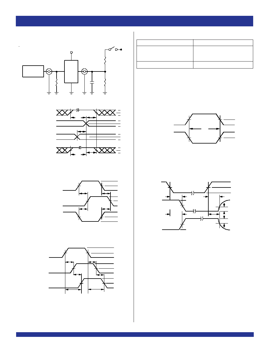
SWITCHING CHARACTERISTICS OVER OPERATING RANGE
NOTES:
1. See test circuit and waveforms.
2. Minimum limits are guaranteed but not tested on Propagation Delays.
3. This parameter is guaranteed but not production tested.
5
IDT74FCT162344AT/CT/ET
FAST CMOS ADDRESS/CLOCK DRIVER
INDUSTRIAL TEMPERATURE RANGE
Pulse
Generator
R
T
D.U.T
.
V
CC
V
IN
C
L
V
OU
T
50pF
500
500
7.0V
3V
1.5V
0V
3V
1.5V
0V
3V
1.5V
0V
3V
1.5V
0V
DATA
INPUT
TIMING
INPUT
ASYNCHRONOUS CONTROL
PRESET
CLEAR
ETC.
SYNCHRONOUS CONTROL
t
SU
t
H
t
REM
t
SU
t
H
HIGH-LOW-HIGH
PULSE
LOW-HIGH-LOW
PULSE
t
W
1.5V
1.5V
SAME PHASE
INPUT TRANSITION
3V
1.5V
0V
1.5V
V
OH
t
PLH
OUTPU
T
OPPOSITE PHASE
INPUT TRANSITION
3V
1.5V
0V
t
PLH
t
PHL
t
PHL
V
O
L
CONTROL
INPUT
3V
1.5V
0V
3.5V
0V
OUTPUT
NORMALLY
LOW
OUTPUT
NORMALLY
HIGH
SWITCH
CLOSED
SWITCH
OPEN
V
O
L
0.3V
0.3V
t
PL
Z
t
PZ
L
t
PZH
t
PHZ
3.5V
0V
1.5V
1.5V
ENABLE
DISABLE
V
OH
PRESET
CLEAR
CLOCK ENABLE
ETC.
t
PLH1
OUTPUT 1
OUTPUT 2
t
SK1(o
)
t
PLH2
3V
0V
V
OH
1.5V
1.5V
V
O
L
V
OH
1.5V
V
O
L
INPUT
t
PHL1
t
PHL2
t
SK1(o
)
t
SKn(o)
=
|t
PLH2 -
t
PLH1
|
or
|t
PHL2 -
t
PLH1
|
TEST CIRCUITS AND WAVEFORMS
Propagation Delay
Test Circuits for All Outputs
Enable and Disable Times
Set-up, Hold, and Release Times
Pulse Width
Output Skew ≠ t
SKn(o)
Test
Switch
Open Drain
Disable Low
Closed
Enable Low
All Other Tests
Open
SWITCH POSITION
DEFINITIONS:
C
L
= Load capacitance: includes jig and probe capacitance.
R
T
= Termination resistance: should be equal to Z
OUT
of the Pulse Generator.
NOTES:
1. Diagram shown for input Control Enable-LOW and input Control Disable-HIGH.
2. Pulse Generator for All Pulses: Rate
1.0MHz; t
F
2.5ns; t
R
2.5ns.
NOTES:
1. For t
SK1(o)
OUTPUT1 and OUTPUT2 are in the same bank.
2. For t
SK2(o)
OUTPUT1 and OUTPUT2 are in different banks on the same part.
6
INDUSTRIAL TEMPERATURE RANGE
IDT74FCT162344AT/CT/ET
FAST CMOS ADDRESS/CLOCK DRIVER
ORDERING INFORMATION
IDT XX
Temp. Range
XXXX
Device Type
XX
Package
PV
PA
Shrink Small Outline Package
Thin Shrink Small Outline Package
Address/Clock Driver
74
≠
40
∞
C to +85
∞
C
162
Double-Density, 5 Volt, Balanced Drive
FCT
XXX
Family
344AT
344CT
344ET
DATA SHEET DOCUMENT HISTORY
1/21/2002
Removed Military temp grade
5/21/2002
Removed TVSOP package
CORPORATE HEADQUARTERS
for SALES:
for Tech Support:
2975 Stender Way
800-345-7015 or 408-727-6116
logichelp@idt.com
Santa Clara, CA 95054
fax: 408-492-8674
(408) 654-6459
www.idt.com