
1
IDT54/74FCT162511AT/CT
FAST CMOS 16-BIT REGISTERED/LATCHED TRANSCEIVER
MILITARY AND INDUSTRIAL TEMPERATURE RANGES
MAY 2001
IDT54/74FCT162511AT/CT
MILITARY AND INDUSTRIAL TEMPERATURE RANGES
FAST CMOS 16-BIT
REGISTERED/LATCHED
TRANSCEIVER WITH PARITY
DESCRIPTION:
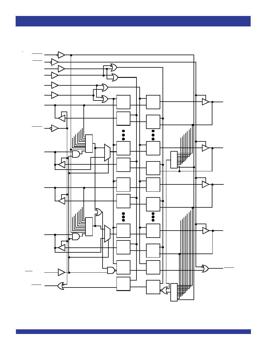
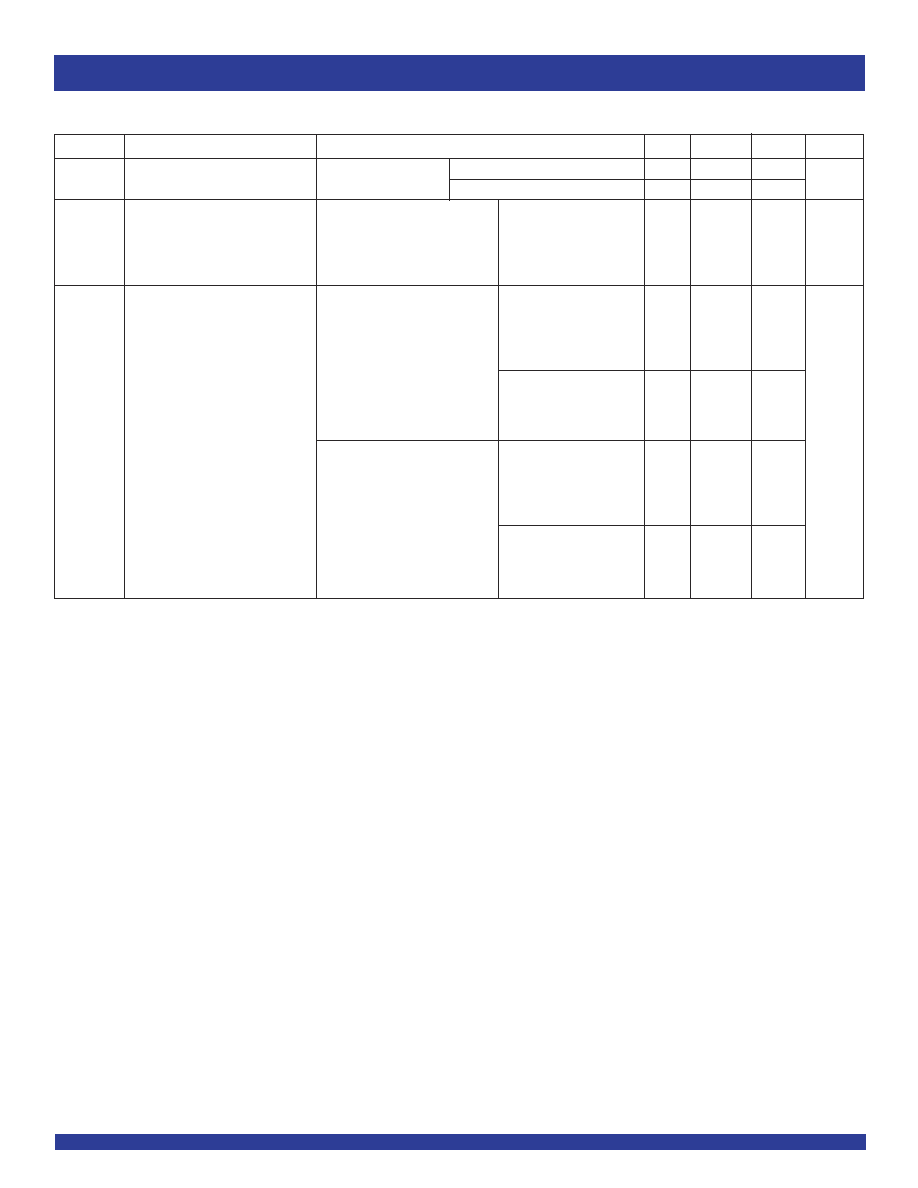
The FCT162511T 16-bit registered/latched transceiver with parity is built
using advanced dual metal CMOS technology. This high-speed, low-power
transceiver combines D-type latches and D-type flip-flops to allow data flow in
transparent, latched, or clocked modes. The device has a parity generator/
checker in the A-to-B direction and a parity checker in the B-to-A direction. Error
checking is done at the byte level with separate parity bits for each byte. Separate
error flags exits for each direction with a single error flag indicating an error for
either byte in the A-to-B direction and a second error flag indicating an error for
either byte in the B-to-A direction. The parity error flags are open drain outputs
which can be tied together and/or tied with flags from other devices to form a single
error flag or interrupt. The parity error flags are enabled by the OExx control
pins allowing the designer to disable the error flag during combinational
transitions.
The control pins LEAB, CLKAB, and OEAB control operation in the A-to-B
direction while LEBA, CLKBA, and OEBA control the B-to-A direction. GEN/
CHK is only for the selection of A-to-B operation. The B-to-A direction is always
in checking mode. The ODD/EVEN select is common between the two directions.
Except for the ODD/EVEN control, independent operation can be achieved
between the two directions by using the corresponding control lines.
GEN /C H K
Latch/
R egister
Byte
Parity
Generator/
Checker
Latch/
Register
Byte
Parity
Checking
B0-15
A0-15
PA1,2
PB1,2
PER B
LEA B
CLKAB
OEAB
OEBA
PER A
LEB A
CLKB A
Parity, data
Parity, data
Parity, Data
Data
(Open D rain)
(Open Drain)
Parity
ODD/EVEN
16
18
18
18
2
The IDT logo is a registered trademark of Integrated Device Technology, Inc.
© 2001 Integrated Device Technology, Inc.
DSC-2916/-
FEATURES:
∑ 0.5 MICRON CMOS Technology
∑ Typical t
sk(o)
(Output Skew) < 250ps, clocked mode
∑ Low input and output leakage
1µA (max)
∑ ESD > 2000V per MIL-STD-883, Method 3015; > 200V using
machine model (C = 200pF, R = 0)
∑ V
CC
= 5V ±10%
∑ Balanced Output Drivers:
≠ ±24mA (industrial)
≠ ±16mA (military)
∑ Series current limiting resistors
∑ Generate/Check, Check/Check modes
∑ Open drain parity error allows wire-OR
∑ Available in the following packages:
≠ Industrial: SSOP, TSSOP
≠ Military: CERPACK
FUNCTIONAL BLOCK DIAGRAM
2
MILITARY AND INDUSTRIAL TEMPERATURE RANGES
IDT54/74FCT162511AT/CT
FAST CMOS 16-BIT REGISTERED/LATCHED TRANSCEIVER
BLOCK DIAGRAM
A
8
- A
15
GEN/C HK
OEAB
CLKB A
LEBA
C LKA B
A
0
- A
7
LEA B
B
0
- B
7
D
C
C
D
OEBA
D
C
B
8
- B
15
D
C
C
D
PB
2
PA
2
C
D
C
D
P
C
D
C
D
PER B
D
C
D
C
PB
1
PA
1
C
D
C
D
P
(Open Drain)
D
C
D
C
D
C
D
C
D
C
D
C
D
C
ODD/EVEN
(Open D rain)
PER A
P
P
I
O
I
O
3
IDT54/74FCT162511AT/CT
FAST CMOS 16-BIT REGISTERED/LATCHED TRANSCEIVER
MILITARY AND INDUSTRIAL TEMPERATURE RANGES
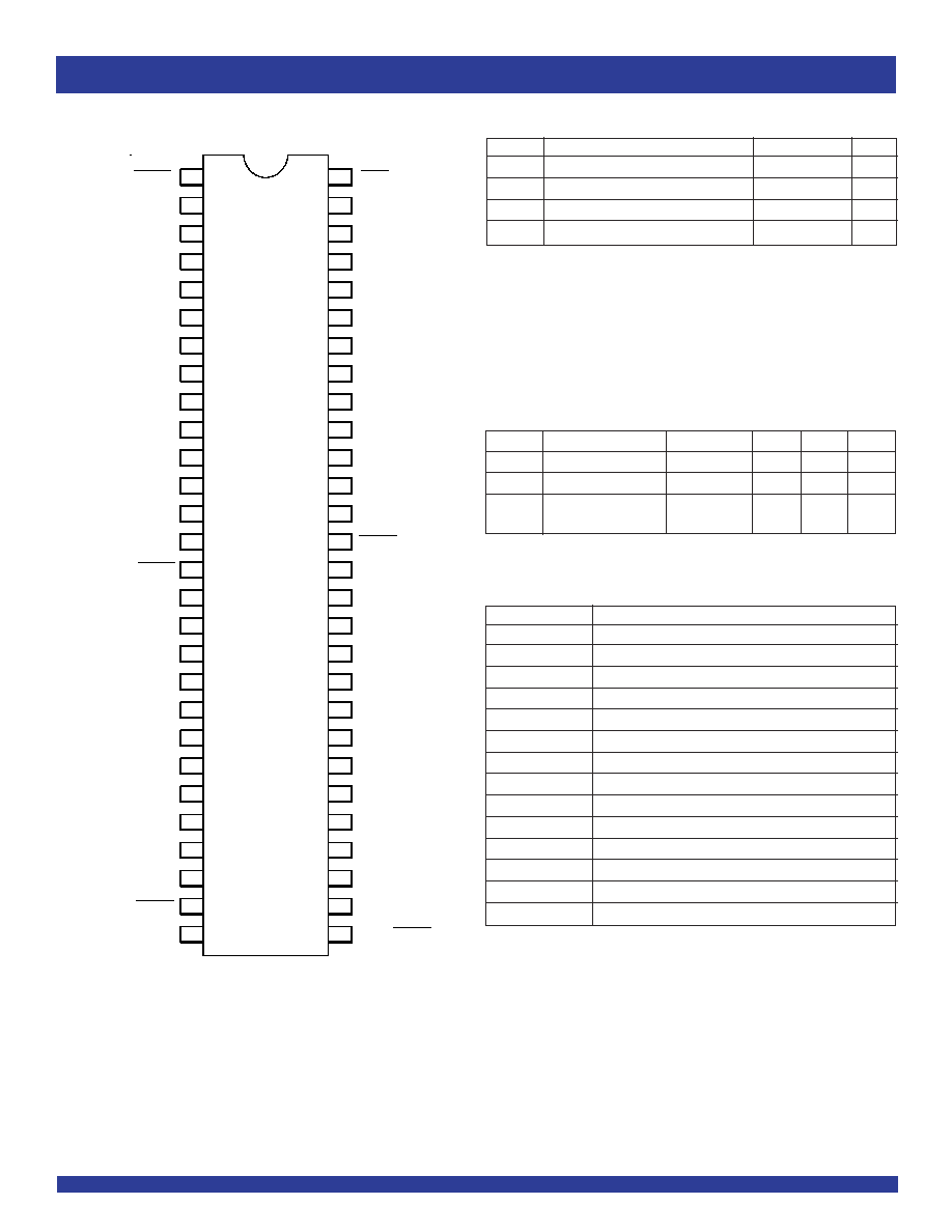
SSOP/ TSSOP/ CERPACK
TOP VIEW
PIN CONFIGURATION
GEN/CHK
B
0
B
1
GND
B
2
B
3
V
CC
B
4
B
6
PB
1
B
7
PERB
GND
B
8
B
5
B
9
B
11
V
CC
B
12
B
10
CLKAB
B
14
B
13
B
15
GND
PB
2
CLKBA
ODD/EVEN
OEAB
LEAB
PA
1
GND
A
0
A
1
V
CC
A
2
A
3
A
5
A
4
A
6
A
7
GND
A
10
PERA
A
8
V
CC
A
9
PA
2
A
12
A
11
A
14
GND
A
15
LEBA
A
13
OEBA
47
37
38
39
40
41
42
43
44
45
46
33
34
35
36
56
55
49
50
51
52
53
54
48
1
2
3
4
5
6
7
8
9
10
12
13
14
15
16
17
18
19
20
11
21
22
23
24
29
30
31
32
25
26
27
28
Symbol
Description
Max
Unit
V
TERM
(2)
Terminal Voltage with Respect to GND
≠0.5 to 7
V
V
TERM
(3)
Terminal Voltage with Respect to GND
≠0.5 to V
CC
+0.5
V
T
STG
Storage Temperature
≠65 to +150
∞C
I
OUT
DC Output Current
≠60 to +120
mA
ABSOLUTE MAXIMUM RATINGS
(1)
(1)
(1)
(1)
(1)
NOTES:
1. Stresses greater than those listed under ABSOLUTE MAXIMUM RATINGS may cause
permanent damage to the device. This is a stress rating only and functional operation
of the device at these or any other conditions above those indicated in the operational
sections of this specification is not implied. Exposure to absolute maximum rating
conditions for extended periods may affect reliability.
2. All device terminals except FCT162XXX Output and I/O terminals.
3. Output and I/O terminals for FCT162XXX.
Symbol
Parameter
(1)
Conditions
Typ.
Max.
Unit
C
IN
Input Capacitance
V
IN
= 0V
3.5
6
pF
C
I/O
I/O Capacitance
V
OUT
= 0V
3.5
8
pF
C
O
Open Drain
V
OUT
= 0V
3.5
6
pF
Capacitance
CAPACITANCE
(T
A
= +25∞C, F = 1.0MHz)
PIN DESCRIPTION
Pin Names
Description
OEAB
A-to-B Output Enable Input (Active LOW)
OEBA
B-to-A Output Enable Input (Active LOW)
LEAB
A-to-B Latch Enable Input
LEBA
B-to-A Latch Enable Input
CLKAB
A-to-B Clock Input
CLKBA
B-to-A Clock Input
A x
A-to-B Data Inputs or B-to-A 3-State Outputs
B x
B-to-A Data Inputs or A-to-B 3-State Outputs
PERA
Parity Error (Open Drain) on A Outputs
PERB
Parity Error (Open Drain) on B Outputs
PAx
(1)
A-to-B Parity Input, B-to-A Parity Output
PBx
B-to-A Parity Input, A-to-B Parity Output
ODD/EVEN
Parity Mode Selection Input
GEN/CHK
A to B Port Generate or Check Mode Input
NOTE:
1. The PAx pin input is internally disabled during parity generation. This means that when
generating parity in the A to B direction there is no need to add a pull up resistor to
guarantee state. The pin will still function properly as the parity output for the B to A
direction.
4
MILITARY AND INDUSTRIAL TEMPERATURE RANGES
IDT54/74FCT162511AT/CT
FAST CMOS 16-BIT REGISTERED/LATCHED TRANSCEIVER
NOTES:
1. Conditions shown are for GEN/CHK = H, OEAB = L, OEBA = H.
2. A-to-B parity checking is shown. B-to-A parity checking is similar but uses OEBA = L, OEAB
= H and errors will be indicated on PERA.
3. In parity checking mode the parity bits will be transmitted unchanged along with the
corresponding data regardless of parity errors (PB1 = PA1).
4. The response shown is for LEAB = H. If LEAB = L then CLKAB will control as an edge triggered
clock.
5. Conditions shown are for the byte A0≠A7 and PA1. The byte A8≠A15 and PA2 is similiar.
6. The parity error flag PERB is a combined flag for both bytes A0≠A7 and A8≠A15. If a parity
error occurs on either byte PERB will go low. PERB is an open drain output which must
be externally pulled up to achieve a logic HIGH.
NOTES:
1. Conditions shown are for GEN/CHK = L, OEAB = L, OEBA = H.
2. A-to-B parity checking is shown. B-to-A is capable of parity checking while A-to-B
is performing generation. B-to-A will not generate parity.
3. The response shown is for LEAB = H. If LEAB = L then CLKAB will control as an edge
triggered clock.
4. Conditions shown are for the byte A≠A7. The byte A8≠A15 is similiar but will output
the parity on PB2.
5. The error flag PERB will remain in a high state during parity generation.
FUNCTION TABLE
(1, 4)
NOTES:
1. A-to-B data flow is shown. B-to-A data flow is similar but uses OEBA, LEBA,
and CLKBA.
2. Output level before the indicated steady-state input conditions were established.
3. Output level before the indicated steady-state input conditions were established,
provided that CLKAB was HIGH before LEAB went LOW.
4. H = HIGH Voltage Level
L = LOW Voltage Level
X = Don't Care
Z = High-impedance
= LOW-to-HIGH Transition
Inputs
Outputs
OEAB
LEAB
CLKAB
Ax
Bx
H
X
X
X
Z
L
H
X
L
L
L
H
X
H
H
L
L
L
L
L
L
H
H
L
L
L
X
B
(2)
L
L
H
X
B
(3)
A0 ≠ A7
Number of inputs that are high
ODD/EVEN
PB1
1, 3, 5 or 7
L
H
1, 3, 5 or 7
H
L
0, 2, 4, 6 or 8
L
L
0, 2, 4, 6 or 8
H
H
A
0
≠ A
7
and P
A1(5)
Number of inputs that are high
ODD/EVEN
PERB
1, 3, 5, 7 or 9
L
L
1, 3, 5, 7 or 9
H
H
(6)
0, 2, 4, 6 or 8
L
H
(6)
0, 2, 4, 6 or 8
H
L
FUNCTION TABLE
(PARITY CHECKING)
(1, 2, 3, 4)
FUNCTION TABLE
(PARITY GENERATION)
(1, 2, 3, 4, 5)
5
IDT54/74FCT162511AT/CT
FAST CMOS 16-BIT REGISTERED/LATCHED TRANSCEIVER
MILITARY AND INDUSTRIAL TEMPERATURE RANGES
Symbol
Parameter
Test Conditions
(1)
Min.
Typ.
(2)
Max.
Unit
V
IH
Input HIGH Level
Guaranteed Logic HIGH Level
2
--
--
V
V
IL
Input LOW Level
Guaranteed Logic LOW Level
--
--
0.8
V
I
IH
Input HIGH Current (Input pins)
(5)
V
CC
= Max.
V
I
= V
CC
--
--
±1
µA
Input HIGH Current (I/O pins)
(5)
--
--
±1
I
IL
Input LOW Current (Input pins)
(5)
V
I
= GND
--
--
±1
Input LOW Current (I/O pins)
(5)
--
--
±1
I
OZH
High Impedance Output Current
V
CC
= Max.
V
O
= 2.7V
--
--
±1
µA
I
OZL
(3-State Output pins)
(5)
V
O
= 0.5V
--
--
±1
V
IK
Clamp Diode Voltage
V
CC
= Min., I
IN
= ≠18mA
--
≠0.7
≠1.2
V
I
OS
Short Circuit Current
V
CC
= Max., V
O
= GND
(3)
≠80
≠140
≠250
mA
V
H
Input Hysteresis
--
--
100
--
mV
I
CCL
Quiescent Power Supply Current
V
CC
= Max.
--
5
500
µA
I
CCH
V
IN
= GND or V
CC
I
CCZ
DC ELECTRICAL CHARACTERISTICS OVER OPERATING RANGE
Following Conditions Apply Unless Otherwise Specified:
Industrial: T
A
= ≠40∞C to +85∞C, V
CC
= 5.0V ±10%; Military: T
A
= ≠55∞C to +125∞C, V
CC
= 5.0V ±10%
NOTES:
1. For conditions shown as Min. or Max., use appropriate value specified under Electrical Characteristics for the applicable device type.
2. Typical values are at V
CC
= 5.0V, +25∞C ambient.
3. Not more than one output should be shorted at one time. Duration of the test should not exceed one second.
4. Duration of the condition can not exceed one second.
5. The test limit for this parameter is ±5µA at T
A
= ≠55∞C.
OUTPUT DRIVE CHARACTERISTICS
Symbol
Parameter
Test Conditions
(1)
Min.
Typ.
(2)
Max.
Unit
I
ODL
Output LOW
(I/O pins)
V
CC
= 5V, V
IN
= V
IH
or V
IL
, V
O
= 1.5V
(3)
60
115
200
mA
Current
(Open Drain)
--
250
--
mA
I
ODH
Output HIGH Current
V
CC
= 5V, V
IN
= V
IH
or V
IL
, V
O
= 1.5V
(3)
≠60
≠115
≠200
mA
I
OFF
Output Power Off Leakage Current
V
CC
= 0, V
O
5.5V
--
--
±1
µA
(Open Drain)
(5)
V
OH
Output HIGH Voltage (I/O pins)
V
CC
= Min.
I
OH
= ≠16mA MIL
2.4
3.3
--
V
V
IN
= V
IH
or V
IL
I
OH
= ≠24mA IND
V
OL
Output LOW
(I/O pins)
V
CC
= Min.
I
OL
= 16mA MIL
--
0.3
0.55
V
Voltage
V
IN
= V
IH
or V
IL
I
OL
= 24mA IND
(Open Drain)
I
OL
= 48mA MIL
--
0.3
0.55
V
I
OL
= 64mA IND
6
MILITARY AND INDUSTRIAL TEMPERATURE RANGES
IDT54/74FCT162511AT/CT
FAST CMOS 16-BIT REGISTERED/LATCHED TRANSCEIVER
Symbol
Parameter
Test Conditions
(1)
Min.
Typ.
(2)
Max.
Unit
I
CC
Quiescent Power Supply Current
V
CC
= Max.
All other Input Pins
--
0.5
1.5
mA
TTL Inputs HIGH
V
IN
= 3.4V
(3)
Parity Input Pins (PAx, PBx)
--
1
2.5
I
CCD
Dynamic Power Supply
V
CC
= Max.
V
IN
= V
CC
--
75
120
µA/
Current
(4)
Outputs Open
V
IN
= GND
MHz
OEAB = GND, OEBA = V
CC
One Input Togging
50% Duty Cycle
I
C
Total Power Supply Current
(6)
V
CC
= Max.
V
IN
= V
CC
--
0.8
1.7
mA
Outputs Open
V
IN
= GND
f
CP
= 10MHz (CLKAB)
50% Duty Cycle
OEAB = GND, OEBA = V
CC
LEAB = GND
V
IN
= 3.4V
--
1.3
3.2
One Bit Toggling
V
IN
= GND
f
i
= 5MHz
50% Duty Cycle
V
CC
= Max.
V
IN
= V
CC
--
3.8
6.5
(5)
Outputs Open
V
IN
= GND
f
CP
= 10MHz (CLKAB)
50% Duty Cycle
OEAB = GND, OEBA = V
CC
LEAB = GND
V
IN
= 3.4V
--
9
21.8
(5)
Eighteen Bits Toggling
V
IN
= GND
f
i
= 2.5MHz
50% Duty Cycle
POWER SUPPLY CHARACTERISTICS
NOTES:
1. For conditions shown as Min. or Max., use appropriate value specified under Electrical Characteristics for the applicable device type.
2. Typical values are at V
CC
= 5.0V, +25∞C ambient.
3. Per TTL driven input (V
IN
= 3.4V). All other inputs at V
CC
or GND.
4. This parameter is not directly testable, but is derived for use in Total Power Supply Calculations.
5. Values for these conditions are examples of the I
CC
formula. These limits are guaranteed but not tested.
6. I
C
= I
QUIESCENT
+ I
INPUTS
+ I
DYNAMIC
I
C
= I
CC
+
I
CC
D
H
N
T
+ I
CCD
(f
CP
N
CP
/2 + fiNi)
I
CC
= Quiescent Current (I
CCL
, I
CCH
and I
CCZ
)
I
CC
= Power Supply Current for a TTL High Input (V
IN
= 3.4V)
D
H
= Duty Cycle for TTL Inputs High
N
T
= Number of TTL Inputs at D
H
I
CCD
= Dynamic Current caused by an Input Transition Pair (HLH or LHL)
f
CP
= Clock Frequency for Register Devices (Zero for Non-Register Devices)
N
CP
= Number of Clock Inputs at f
CP
fi = Input Frequency
Ni = Number of Inputs at fi
7
IDT54/74FCT162511AT/CT
FAST CMOS 16-BIT REGISTERED/LATCHED TRANSCEIVER
MILITARY AND INDUSTRIAL TEMPERATURE RANGES
FCT162511AT
FCT162511CT
Ind.
Mil.
Ind.
Mil.
Symbol Parameter
Condition
(1)
Min.
(2)
Max.
Min.
(2)
Max.
Min.
(2)
Max.
Min.
(2)
Max.
Unit
t
PLH
Propagation Delay, PAx to PBx
C
L
= 50pF
1.5
5
1.5
5.3
1.5
4.2
1.5
4.5
ns
t
PHL
Ax to Bx or Bx to Ax, PBx to PAx
R
L
= 500
t
PLH
Propagation Delay
GEN/CHK LOW
1.5
7.5
1.5
8
1.5
6.5
1.5
6.8
ns
t
PHL
Ax to PBx
t
PLH(3)
Propagation Delay
1.5
9
1.5
9
1.5
7.5
1.5
7.8
ns
t
PHL
Ax to PERB, PAx to PERB
1.5
8
1.5
8
1.5
6.5
1.5
6.8
ns
t
PLH(3)
Propagation Delay
1.5
9
1.5
9
1.5
7.5
1.5
7.8
ns
t
PHL
Bx to PERA, PBx to PERA
1.5
8
1.5
8
1.5
6.5
1.5
6.8
ns
t
PLH
Propagation Delay
t
PHL
LEBA to Ax and PAx
1.5
5.6
1.5
6
1.5
5.3
1.5
5.5
ns
LEAB to Bx and PBx
t
PLH(3)
Propagation Delay
1.5
7
1.5
7
1.5
6
1.5
6.3
ns
t
PHL
LEBA to PERA, LEAB to PERB
1.5
6
1.5
6
1.5
5
1.5
5.3
ns
t
PLH
Propagation Delay
t
PHL
CLKBA to Ax and PAx
1.5
5.6
1.5
6
1.5
5.3
1.5
5.5
ns
CLKAB to Bx and PBx
t
PLH(3)
Propagation Delay
1.5
7
1.5
7
1.5
6
1.5
6.3
ns
t
PHL
CLKBA to PERA
CLKAB to PERB
1.5
6
1.5
6
1.5
5
1.5
5.3
ns
t
PZH
Output Enable Time
t
PZL
OEBA to Ax and PAx
1.5
6
1.5
6.5
1.5
5.6
1.5
5.8
ns
OEAB to Bx and PBx
t
PHZ
Output Disable Time
t
PLZ
OEBA to Ax and PAx
1.5
5.6
1.5
6
1.5
5.2
1.5
5.5
ns
OEAB to Bx and PBx
t
PLZ(3)
Parity ERROR Enable
1.5
6
1.5
6.3
1.5
6
1.5
6.3
ns
t
PZL
OEBA to PERA, OEAB to PERB
1.5
6
1.5
6.3
1.5
6
1.5
6.3
ns
t
PLH(3)
ODD/EVEN to PERx
1.5
10
1.5
10
1.5
10
1.5
10
ns
t
PHL
1.5
10
1.5
10
1.5
10
1.5
10
ns
t
PLH
ODD/EVEN to PBx
1.5
10
1.5
10
1.5
10
1.5
10
ns
t
PHL
SWITCHING CHARACTERISTICS OVER OPERATING RANGE
(PROPAGATION DELAYS)
NOTES:
1. See test circuits and waveforms.
2. Minimum limits are guaranteed but not tested on Propagation Delays.
3. On Open Drain Outputs t
PLH
is measured at V
OUT
= V
OL
+ 0.3V.
8
MILITARY AND INDUSTRIAL TEMPERATURE RANGES
IDT54/74FCT162511AT/CT
FAST CMOS 16-BIT REGISTERED/LATCHED TRANSCEIVER
FCT162511AT
FCT162511CT
Ind.
Mil.
Ind.
Mil.
Symbol
Parameter
Test Conditions
(1, 3)
Min. Max. Min. Max. Min. Max. Min. Max. Unit
t
SU
Set-up Time
GEN/CHK LOW
PBx valid
C
L
= 50pF
4
--
4
--
3
--
3.5
--
ns
HIGH or LOW
PBx not valid
R
L
= 500
3
--
3
--
3
--
3
--
ns
Ax to CLKAB
GEN/CHK HIGH
PERB valid
4
--
4
--
3
--
3
--
ns
PERB not valid
3
--
3
--
3
--
3
--
ns
t
SU
Set-up Time
GEN/CHK HIGH
PERB valid
4
--
4
--
3
--
3
--
ns
PAx to CLKAB
PERB not valid
3
--
3
--
3
--
3
--
ns
t
SU
Set-up Time
PERA valid
4
--
4
--
3
--
3
--
ns
Bx to CLKBA,
PERA not valid
3
--
4
--
3
--
3
--
ns
PBx to CLKBA
t
SU
Set-up Time
CLKAB LOW
PBx valid
3.5
--
3.5
--
3
--
3
--
ns
Ax to LEAB
GEN/CHK LOW
PBx not valid
3
--
3
--
3
--
3
--
ns
CLKAB LOW
PERB valid
3.5
--
3.5
--
3
--
3
--
ns
GEN/CHK HIGH
PERB not valid
3
--
3
--
3
--
3
--
ns
CLKAB HIGH
PBx valid
3.5
--
3.5
--
3
--
3
--
ns
GEN/CHK LOW
PBx not valid
3
--
3
--
3
--
3
--
ns
CLKAB HIGH
PERB valid
3.5
--
3.5
--
3
--
3
--
ns
GEN/CHK HIGH
PERB not valid
3
--
3
--
3
--
3
--
ns
t
SU
Set-up Time
CLKAB LOW
PERB valid
3.5
--
3.5
--
3
--
3
--
ns
PAx to LEAB
GEN/CHK HIGH
PERB not valid
3
--
3
--
3
--
3
--
ns
CLKAB HIGH
PERB valid
3.5
--
3.5
--
3
--
3
--
ns
GEN/CHK HIGH
PERB not valid
3
--
3
--
3
--
3
--
ns
t
SU
Set-up Time
CLKBA LOW
PERA valid
3.5
--
3.5
--
3
--
3
--
ns
Bx to LEBA
PERA not valid
3
--
3
--
3
--
3
--
ns
PBx to LEBA
CLKBA HIGH
PERA valid
3.5
--
3.5
--
3
--
3
--
ns
PERA not valid
3
--
3
--
3
--
3
--
ns
t
SK(O)
Output Skew
(4)
--
0.5
--
0.5
--
0.5
--
0.5
ns
SWITCHING CHARACTERISTICS OVER OPERATING RANGE (SET UP TIMES)
FCT162511AT
FCT162511CT
Ind.
Mil.
Ind.
Mil.
Symbol
Parameter
Condition
(1)
Min. Max. Min. Max. Min. Max. Min. Max. Unit
t
H
Hold Time HIGH or LOW Ax to LEAB, Bx to LEBA
C
L
= 50pF
1
--
1
--
1
--
1
--
ns
t
H
Hold Time HIGH or LOW PAx to LEAB
R
L
= 500
1
--
1
--
1
--
1
--
ns
t
H
Hold Time HIGH or LOW PBx to LEBA
1
--
1
--
1
--
1
--
ns
t
H
Hold Time Ax to CLKAB, PAx to CLKAB
1
--
1
--
0
--
0
--
ns
t
H
Hold Time Bx to CLKBA, PBx to CLKBA
1
--
1
--
0
--
0
--
ns
t
W
LEAB or LEBA Pulse Width HIGH
(2)
3
--
3
--
3
--
3
--
ns
t
W
CLKAB or CLKBA Pulse Width HIGH or LOW
(2)
3
--
3
--
3
--
3
--
ns
SWITCHING CHARACTERISTICS OVER OPERATING RANGE (HOLD TIMES)
NOTES:
1. See test circuits and waveforms.
2. This parameter is guaranteed but not tested.
3. "Not valid" means the set-up time indicated is not sufficient to assure proper functioning of this output; however, the set-up time indicated will assure proper functioning of the
A to B or B to A port respective to the indicated direction.
4. Skew between any two outputs of the same package, switching in the same direction, excluding PERx in clocked mode, and Pxx (parity bits) and PERx in transparent/
latched mode. This parameter is guaranteed by design.
9
IDT54/74FCT162511AT/CT
FAST CMOS 16-BIT REGISTERED/LATCHED TRANSCEIVER
MILITARY AND INDUSTRIAL TEMPERATURE RANGES
Pulse
Generator
R
T
D.U.T.
V
CC
V
IN
C
L
V
OUT
50pF
500
500
7.0V
3V
1.5V
0V
3V
1.5V
0V
3V
1.5V
0V
3V
1.5V
0V
DATA
INPU T
TIMING
INPU T
ASYN CHR ONOU S C ON TR OL
PRESET
CLEAR
ETC .
SYNCH RON OUS CON TR OL
t
SU
t
H
t
RE M
t
SU
t
H
PRESET
CLEAR
C LOCK ENABLE
ETC .
HIGH-LOW -HIGH
PULSE
LOW -HIGH-LOW
PULSE
t
W
1.5V
1.5V
SAM E PHA SE
IN PU T TRAN SITION
3V
1.5V
0V
1.5V
V
OH
t
PLH
OUTPU T
OPPOS ITE P HASE
IN PU T TRAN SITION
3V
1.5V
0V
t
P LH
t
PH L
t
PH L
V
OL
CONTR OL
INPUT
3V
1.5V
0V
3.5V
0V
OUTPUT
N ORM ALLY
LOW
OUTPUT
N ORM ALLY
HIGH
SW ITCH
CLOSED
SW ITC H
OPEN
V
O L
0.3V
0.3V
t
PLZ
t
P ZL
t
PZH
t
PHZ
3.5V
0V
1.5V
1.5V
ENABLE
DISABLE
V
O H
TEST CIRCUITS AND WAVEFORMS
Propagation Delay
Test Circuits for All Outputs
Enable and Disable Times
Set-up, Hold, and Release Times
Pulse Width
Test
Switch
Open Drain
Disable Low
Closed
Enable Low
All Other Tests
Open
SWITCH POSITION
DEFINITIONS:
C
L
= Load capacitance: includes jig and probe capacitance.
R
T
= Termination resistance: should be equal to Z
OUT
of the Pulse Generator.
NOTES:
1. Diagram shown for input Control Enable-LOW and input Control Disable-HIGH.
2. Pulse Generator for All Pulses: Rate
1.0MHz; t
F
2.5ns; t
R
2.5ns.
10
MILITARY AND INDUSTRIAL TEMPERATURE RANGES
IDT54/74FCT162511AT/CT
FAST CMOS 16-BIT REGISTERED/LATCHED TRANSCEIVER
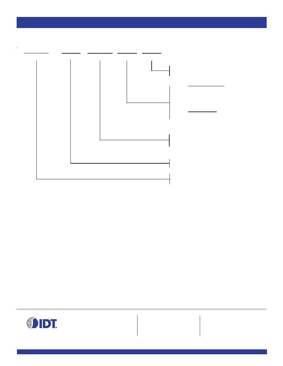
ORDERING INFORMATION
IDT XX
Temp. Range
XXXX
Device Type
XX
Package
X
Process
PV
PA
Industrial Options
Shrink Small Outline Package
Thin Shrink Small Outline Package
18-Bit Registered/Latched Transceiver
54
74
≠ 55∞C to +125∞C
≠ 40∞C to +85∞C
162
Double-Density, 5 Volt, Balanced Drive
E
Military Options
CERPACK
Blank
B
Industrial
MIL-STD-883, Class B
FCT
XXX
Family
511AT
511CT
CORPORATE HEADQUARTERS
for SALES:
for Tech Support:
2975 Stender Way
800-345-7015 or 408-727-6116
logichelp@idt.com
Santa Clara, CA 95054
fax: 408-492-8674
(408) 654-6459
www.idt.com