1
IDT74FCT162H272AT/CT
FAST CMOS 12-BIT SYNCHRONOUS BUS EXCHANGER
INDUSTRIAL TEMPERATURE RANGE
NOVEMBER 2002
IDT74FCT162H272AT/CT
INDUSTRIAL TEMPERATURE RANGE
FAST CMOS 12-BIT
SYNCHRONOUS
BUS EXCHANGER
DESCRIPTION:
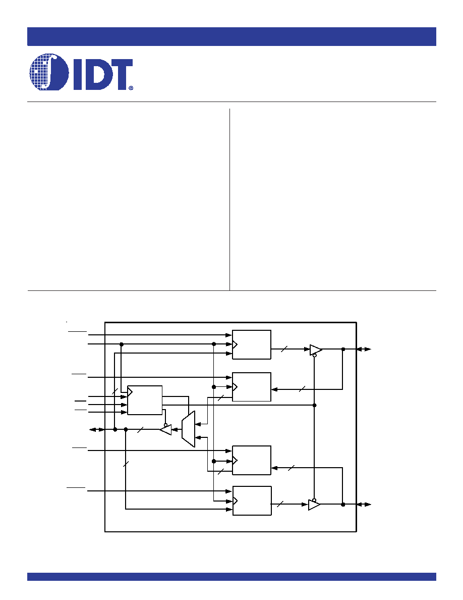
The FCT162H272T synchronous tri-port bus exchangers are high-speed,
bidirectional,12-bit, registered, bus multiplexers for use in synchronous memory
interleaving applications. All registers have a common clock and use a clock
enable (CExxx) on each data register to control data sequencing. The output
enables and mux select (OEA, OEB and SEL) are also under synchronous
control allowing direction changes to be edge triggered events.
The tri-port bus exchanger has three 12-bit ports. Data may be transferred
between the A port and either/both of the B ports. The clock enable (CE1B,
CE2B, CEA1B and CEA2B) inputs control the data storage. Both B ports have
a common output enable (OEB) to aid in synchronously loading the B registers
from the B port.
The FCT162H272T has balanced output drive with current limiting resistors.
This offers low ground bounce, minimal undershoot, and controlled output fall
times-reducing the need for external series terminating resistors.
The FCT162H272T has "Bus Hold" which retains the input's last state
whenever the input goes to high impedance. This prevents "floating" inputs and
eliminates the need for pull-up/down resistors.
A-1B
REG ISTER
CLK
SEL
12
M
U
X
12
12
A
1:12
1B
1:12
12
12
12
12
12
2B
1:12
CE1B
CEA1B
1
0
O EB
O EA
CE2B
CEA2B
1B-A
REG ISTER
12
2B-A
REGISTER
A-2B
REGISTER
C ONTROL
REG ISTER
CE
D
Q
CE
D
Q
CE
D
Q
CE
D
Q
FEATURES:
∑ 0.5 MICRON CMOS Technology
∑ Typical t
SK(o)
(Output Skew) < 250ps
∑ Low input and output leakage
1µA (max.)
∑ ESD > 2000V per MIL-STD-883, Method 3015; > 200V using
machine model (C = 200pF, R = 0)
∑ Balanced Output Drivers: ±24mA
∑ Reduced system switching noise
∑ Typical V
OLP
(Output Ground Bounce) < 0.6V at V
CC
= 5V,
T
A
= 25∞C
∑ Bus Hold retains last active bus state during 3-state
∑ Eliminates the need for external pull up resistors
∑ Available in SSOP and TSSOP packages
FUNCTIONAL BLOCK DIAGRAM
The IDT logo is a registered trademark of Integrated Device Technology, Inc.
© 2002 Integrated Device Technology, Inc.
DSC-3071/1
2
INDUSTRIAL TEMPERATURE RANGE
IDT74FCT162H272AT/CT
FAST CMOS 12-BIT SYNCHRONOUS BUS EXCHANGER
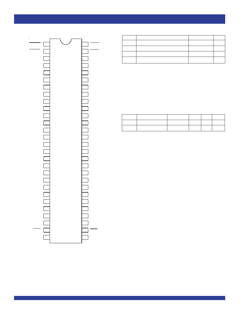
SSOP/ TSSOP
TOP VIEW
PIN CONFIGURATION
CEA1B
CEA2B
GN D
2B
2
V
CC
A
3
A
6
A
7
GN D
A
1 2
2B
3
2B
1
A
1
A
2
GN D
A
4
A
5
A
8
A
9
A
1 0
V
CC
1B
1
A
1 1
1B
2
CE2B
2B
4
GND
2B
5
2B
6
V
C C
2B
7
2B
8
GND
2B
10
2B
11
2B
12
1B
11
1B
10
GND
1B
9
V
C C
1B
6
1B
8
2B
9
1B
12
1B
7
1B
5
CE1B
39
29
30
31
32
33
34
35
36
37
38
25
26
27
28
48
47
41
42
43
44
45
46
40
1
2
3
4
5
6
7
8
9
10
12
13
14
15
16
17
18
19
20
11
21
22
23
24
SO56-1
SO56-2
OEA
GN D
SEL
1B
3
CLK
GND
1B
4
OEB
49
56
55
50
51
52
53
54
Symbol
Description
Max
Unit
V
TERM(2)
Terminal Voltage with Respect to GND
≠0.5 to 7
V
V
TERM(3)
Terminal Voltage with Respect to GND
≠0.5 to V
CC
+0.5
V
T
STG
Storage Temperature
≠65 to +150
∞C
I
OUT
DC Output Current
≠60 to +120
mA
ABSOLUTE MAXIMUM RATINGS
(1)
NOTES:
1. Stresses greater than those listed under ABSOLUTE MAXIMUM RATINGS may cause
permanent damage to the device. This is a stress rating only and functional operation
of the device at these or any other conditions above those indicated in the operational
sections of this specification is not implied. Exposure to absolute maximum rating
conditions for extended periods may affect reliability.
2. All device terminals except FCT162XXX Output and I/O terminals.
3. Output and I/O terminals for FCT162XXXT.
Symbol
Parameter
(1)
Conditions
Typ.
Max.
Unit
C
IN
Input Capacitance
V
IN
= 0V
3.5
6
pF
C
OUT
Output Capacitance
V
OUT
= 0V
3.5
8
pF
CAPACITANCE
(T
A
= +25∞C, f = 1.0MHz)
NOTE:
1. This parameter is measured at characterization but not tested.

3
IDT74FCT162H272AT/CT
FAST CMOS 12-BIT SYNCHRONOUS BUS EXCHANGER
INDUSTRIAL TEMPERATURE RANGE
Signal
I/O
Description
A
(1:12)
I/O
Bidirectional Data Port A. Usually connected to the CPU's Address/Data bus.
(1)
1B
(1:12)
I/O
Bidirectional Data Port 1B. Usually connected to the even path or even bank of memory.
(1)
2B
(1:12)
I/O
Bidirectional Data Port 2B. Usually connected to the odd path or odd bank of memory.
(1)
CLK
I
Clock Input
CEA1B
I
Clock Enable Input for the A-1B Register. If CEA1B is LOW during the rising edge of CLK, data will be clocked into register A-1B
(Active LOW).
CEA2B
I
Clock Enable Input for the A-2B Register. If CEA2B is LOW during the rising edge of CLK, data will be clocked into register A-2B
(Active LOW).
CE1B
I
Clock Enable Input for the 1B-A Register. If CE1B is LOW during the rising edge of CLK, data will be clocked into register 1B-A
(Active LOW).
CE2B
I
Clock Enable Input for the 2B-A Register. If CE2B is LOW during the rising edge of CLK, data will be clocked into register 2B-A
(Active LOW).
SEL
I
1B or 2B Path Selection. When HIGH during the rising edge of CLK, SEL enables data transfer from 1B Port to A Port. When LOW during
the rising edge of CLK, SEL enables data transfer from 2B Port to A Port.
OEA
I
Synchronous Output Enable for A Port (Active LOW).
OEB
I
Synchronous Output Enable for 1B Port and 2B Port (Active LOW).
NOTE:
1. On FCT162H272T these pins have "Bus Hold". All other pins are standard inputs, outputs or I/Os.
PIN DESCRIPTION
FUNCTION TABLES
(2)
Inputs
Output
1B
2B
SEL
CE1B CE2B
OEA
CLK
A
H
X
H
L
X
L
H
L
X
H
L
X
L
L
X
X
H
H
X
L
A
(1)
X
H
L
X
L
L
H
X
L
L
X
L
L
L
X
X
L
X
H
L
A
(1)
X
X
X
X
X
H
Z
Inputs
Outputs
A
CEA1B
CEA2B
OEB
CLK
1B
2B
H
L
L
L
H
H
L
L
L
L
L
L
H
L
H
L
H
B
(1)
L
L
H
L
L
B
(1)
H
H
L
L
B
(1)
H
L
H
L
L
B
(1)
L
X
H
H
L
B
(1)
B
(1)
X
X
X
H
Z
Z
X
X
X
L
Active
Active
NOTES:
1. Output level before the indicated steady-state input conditions were established.
2. H = HIGH Voltage Level
L = LOW Voltage Level
X = Don't Care
Z = High-Impedance
= LOW-to-HIGH Transition
4
INDUSTRIAL TEMPERATURE RANGE
IDT74FCT162H272AT/CT
FAST CMOS 12-BIT SYNCHRONOUS BUS EXCHANGER
Symbol
Parameter
Test Conditions
(1)
Min.
Typ.
(2)
Max.
Unit
V
IH
Input HIGH Level
Guaranteed Logic HIGH Level
2
--
--
V
V
IL
Input LOW Level
Guaranteed Logic LOW Level
--
--
0.8
V
I
IH
Input
Standard Input
(5)
V
CC
= Max.
V
I
= V
CC
--
--
±1
µA
HIGH
Standard I/O
(5)
--
--
±1
Current
(4)
Bus-hold Input
--
--
±100
Bus-hold I/O
--
--
±100
I
IL
Input
Standard Input
(5)
V
I
= GND
--
--
±1
LOW
Standard I/O
(5)
--
--
±1
Current
(4)
Bus-hold Input
--
--
±100
Bus-hold I/O
--
--
±100
I
BHH
Bus-hold Sustain
Bus-hold Input
V
CC
= Min.
V
I
= 2V
≠50
--
--
µA
I
BHL
Current
(4)
V
I
= 0.8V
50
--
--
I
OZH
High Impedance Output Current
V
CC
= Max.
V
O
= 2.7V
--
--
±1
µA
I
OZL
(3-State Output pins)
(5, 6)
V
O
= 0.5V
--
--
±1
V
IK
Clamp Diode Voltage
V
CC
= Min., I
IN
= ≠18mA
--
≠0.7
≠1.2
V
I
OS
Short Circuit Current
V
CC
= Max., V
O
= GND
(3)
≠80
≠140
≠250
mA
V
H
Input Hysteresis
--
--
100
--
mV
I
CCL
Quiescent Power Supply Current
V
CC
= Max.
--
5
500
µA
I
CCH
V
IN
= GND or V
CC
I
CCZ
DC ELECTRICAL CHARACTERISTICS OVER OPERATING RANGE (BUS HOLD)
Following Conditions Apply Unless Otherwise Specified:
Industrial: T
A
= ≠40∞C to +85∞C, V
CC
= 5.0V ±10%
OUTPUT DRIVE CHARACTERISTICS
NOTES:
1. For conditions shown as Min. or Max., use appropriate value specified under Electrical Characteristics for the applicable device type.
2. Typical values are at V
CC
= 5.0V, +25∞C ambient.
3. Not more than one output should be shorted at one time. Duration of the test should not exceed one second.
4. Duration of the condition can not exceed one second.
5. This test limit for this parameter is ±5µA at T
A
= ≠55∞C.
6. Does not include Bus-Hold I/O pins.
Symbol
Parameter
Test Conditions
(1)
Min. Typ.
(2)
Max.
Unit
I
ODL
Output LOW Current
V
CC
= 5V, V
IN
= V
IH
or V
IL
, V
O
= 1.5V
(3)
60
115
200
mA
I
ODH
Output HIGH Current
V
CC
= 5V, V
IN
= V
IH
or V
IL
, V
O
= 1.5V
(3)
≠60
≠115
≠200
mA
V
OH
Output HIGH Voltage
V
CC
= Min.
I
OH
= ≠24mA
2.4
3.3
--
V
V
IN
= V
IH
or V
IL
V
OL
Output LOW Voltage
V
CC
= Min.
I
OH
= 24mA
--
0.3
0.55
V
V
IN
= V
IH
or V
IL

5
IDT74FCT162H272AT/CT
FAST CMOS 12-BIT SYNCHRONOUS BUS EXCHANGER
INDUSTRIAL TEMPERATURE RANGE
NOTES:
1. For conditions shown as Min. or Max., use appropriate value specified under Electrical Characteristics for the applicable device type.
2. Typical values are at V
CC
= 5.0V, +25∞C ambient.
3. Per TTL driven input (V
IN
= 3.4V). All other inputs at V
CC
or GND.
4. This parameter is not directly testable, but is derived for use in Total Power Supply Calculations.
5. Values for these conditions are examples of the I
CC
formula. These limits are guaranteed but not tested.
6. I
C
= I
QUIESCENT
+ I
INPUTS
+ I
DYNAMIC
I
C
= I
CC
+
I
CC
D
H
N
T
+ I
CCD
(f
CP
N
CP
/2 + fiNi)
I
CC
= Quiescent Current (I
CCL
, I
CCH
and I
CCZ
)
I
CC
= Power Supply Current for a TTL High Input (V
IN
= 3.4V)
D
H
= Duty Cycle for TTL Inputs High
N
T
= Number of TTL Inputs at D
H
I
CCD
= Dynamic Current caused by an Input Transition Pair (HLH or LHL)
f
CP
= Clock Frequency for Register Devices (Zero for Non-Register Devices)
N
CP
= Number of Clock Inputs at f
CP
fi = Input Frequency
Ni = Number of Inputs at fi
Symbol
Parameter
Test Conditions
(1)
Min.
Typ.
(2)
Max.
Unit
I
CC
Quiescent Power Supply Current
V
CC
= Max.
--
0.5
1.5
mA
TTL Inputs HIGH
V
IN
= 3.4V
(3)
I
CCD
Dynamic Power Supply
V
CC
= Max.
V
IN
= V
CC
--
60
100
µA/
Current
(4)
Outputs Open
V
IN
= GND
MHz
One Output Port Enabled
CExx = GND
One Input Bit Toggling
One Output Bit Toggling
50% Duty Cycle
I
C
Total Power Supply Current
(6)
V
CC
= Max.
V
IN
= V
CC
--
0.6
1
mA
Outputs Open
V
IN
= GND
f
CP
= 10MHz
50% Duty Cycle
OEx = CExx = GND
V
IN
= 3.4V
--
1.1
2.5
One Input Bit Toggling
V
IN
= GND
One Output Bit Toggling
fi = 5MHz
50% Duty Cycle
V
CC
= Max.
V
IN
= V
CC
--
2.1
3.5
(5)
Outputs Open
V
IN
= GND
f
CP
= 10MHz
50% Duty Cycle
OEx = CExx = GND
V
IN
= 3.4V
--
5.4
13.3
(5)
Twelve Input Bits Toggling
V
IN
= GND
Twelve Output Bits Toggling
fi = 2.5MHz
50% Duty Cycle
POWER SUPPLY CHARACTERISTICS
6
INDUSTRIAL TEMPERATURE RANGE
IDT74FCT162H272AT/CT
FAST CMOS 12-BIT SYNCHRONOUS BUS EXCHANGER
FCT162H272AT FCT162H272CT
Symbol
Parameter
Condition
(1)
Min.
(2)
Max.
Min.
(2)
Max.
Unit
t
PLH
Propagation Delay
C
L
= 50pF
1.5
5.8
1.5
5.2
ns
t
PHL
CLK to 1Bx or CLK to 2Bx
R
L
= 500
t
PLH
Propagation Delay
SEL Stable
1.5
6
1.5
5.4
ns
t
PHL
CLK to Ax
CExB Enabled
SEL Changing
1.5
6
1.5
5.4
ns
CExB Disabled
SEL Changing
1.5
7.6
1.5
6.6
ns
CExB Enabled
t
PZH
Output Enable Time
1.5
7.7
1.5
6.8
ns
t
PZL
CLK to Ax, CLK to 1Bx, or CLK to 2Bx
t
PHZ
Output Disable Time
1.5
6.4
1.5
6
ns
t
PLZ
CLK to Ax, CLK to 1Bx, or CLK to 2Bx
t
SU
Set-Up Time, HIGH or LOW Data to CLK
2
--
2
--
ns
t
SU
Set-Up Time, OEA to CLK, OEB to CLK
2
--
2
--
ns
t
SU
Set-Up Time, SEL to CLK
2
--
2
--
ns
t
SU
Set-Up Time, CEA1B to CLK, CE1B to
2
--
2
--
ns
CLK, CE2B to CLK, or CEA2B to CLK
t
H
Hold Time, CLK to Data
0
--
0
--
ns
t
H
Hold Time, CLK to OEA,
0.5
--
0.5
--
ns
CLK to OEB, CLK to SEL
t
H
Hold Time, CLK to CEA1B, CLK to CE1B,
0
--
0
--
ns
CLK to CE2B, CLK to CEA2B
t
W
Pulse Width, CLK HIGH
(3)
3
--
3
--
ns
t
SK(o)
Output Skew
(4)
--
0.5
--
0.5
ns
SWITCHING CHARACTERISTICS OVER OPERATING RANGE
NOTES:
1. See test circuits and waveforms.
2. Minimum limits are guaranteed but not tested on Propagation Delays.
3. This parameter is guaranteed but not tested.
4. Skew between any two outputs of the same package switching in the same direction. This parameter is guaranteed by design.
7
IDT74FCT162H272AT/CT
FAST CMOS 12-BIT SYNCHRONOUS BUS EXCHANGER
INDUSTRIAL TEMPERATURE RANGE
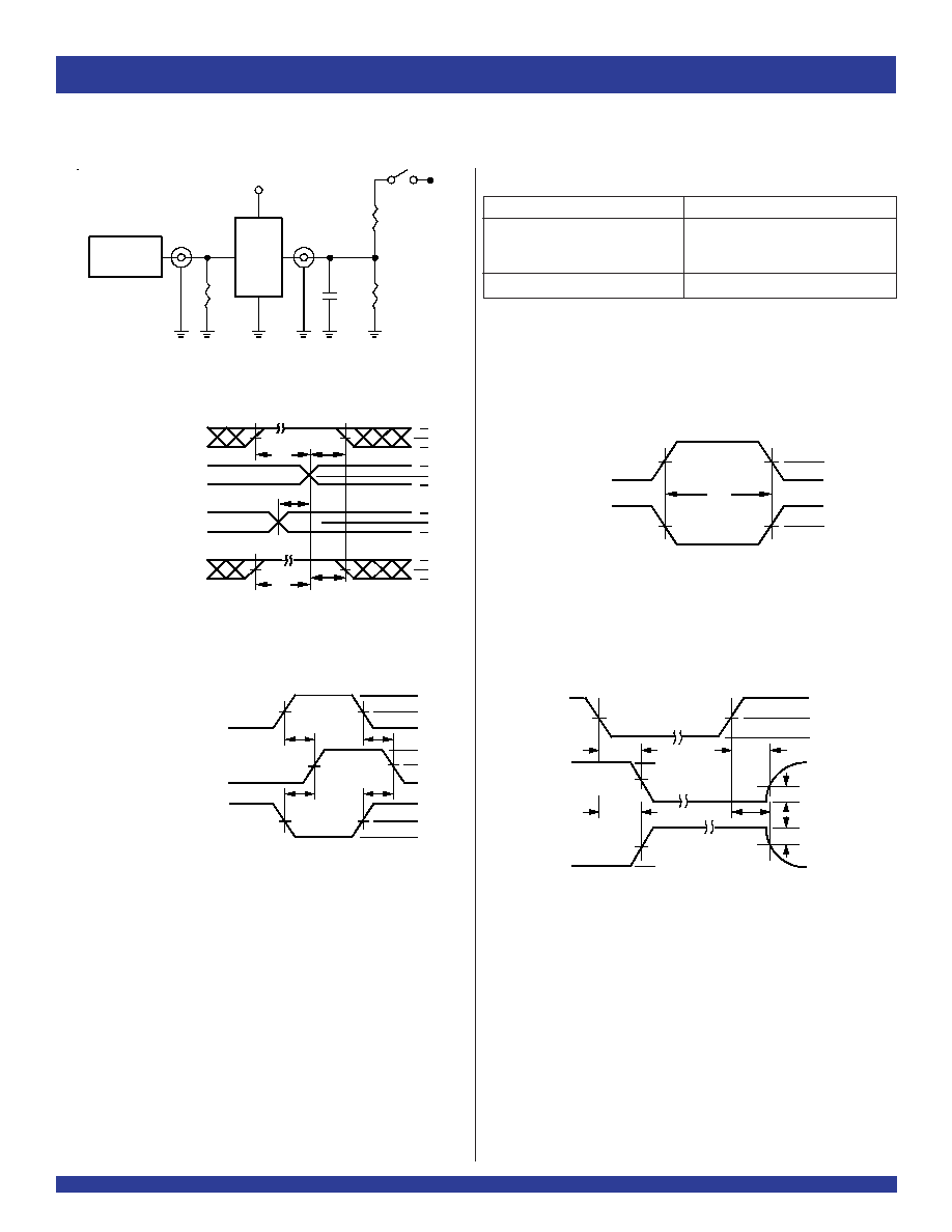
Pulse
Generator
R
T
D.U.T.
V
CC
V
IN
C
L
V
OUT
50pF
500
500
7.0V
3V
1.5V
0V
3V
1.5V
0V
3V
1.5V
0V
3V
1.5V
0V
D ATA
INPUT
TIM IN G
INPUT
ASYNC HR ONOUS C ONTROL
PRES ET
CLEA R
ETC .
SYNCHR ON OUS CONTROL
t
SU
t
H
t
R EM
t
SU
t
H
PRES ET
CLEA R
CLOCK ENABLE
ETC .
HIGH-LOW -H IGH
PU LSE
LOW -HIGH-LOW
PU LSE
t
W
1.5V
1.5V
SAM E PHASE
INPUT TRAN SITION
3V
1.5V
0V
1.5V
V
O H
t
PLH
OU TPU T
OPPOSITE P HASE
INPUT TRAN SITION
3V
1.5V
0V
t
PL H
t
PH L
t
PH L
V
O L
CONTROL
IN PU T
3V
1.5V
0V
3.5V
0V
OUTPU T
NORM ALLY
LOW
OUTPU T
NORM ALLY
H IGH
SW ITCH
C LOSE D
SW ITC H
OPEN
V
OL
0.3V
0.3V
t
PLZ
t
PZL
t
PZH
t
PHZ
3.5V
0V
1.5V
1.5V
ENABLE
D ISABLE
V
OH
TEST CIRCUITS AND WAVEFORMS
Propagation Delay
Test Circuits for All Outputs
Enable and Disable Times
Set-up, Hold, and Release Times
Pulse Width
Test
Switch
Open Drain
Disable Low
Closed
Enable Low
All Other Tests
Open
SWITCH POSITION
DEFINITIONS:
C
L
= Load capacitance: includes jig and probe capacitance.
R
T
= Termination resistance: should be equal to Z
OUT
of the Pulse Generator.
NOTES:
1. Diagram shown for input Control Enable-LOW and input Control Disable-HIGH.
2. Pulse Generator for All Pulses: Rate
1.0MHz; t
F
2.5ns; t
R
2.5ns.
8
INDUSTRIAL TEMPERATURE RANGE
IDT74FCT162H272AT/CT
FAST CMOS 12-BIT SYNCHRONOUS BUS EXCHANGER
ORDERING INFORMATION
ID T
XX
FC T
XXXX
XX
Package
Device Type
Temp. R ange
PV
PA
162
Double-Density, 5 Volt, Balanced Drive
74
Shrink Sm all Outline Package (SO 56-1)
Thin Shrink Sm all O utline Package (SO56-2)
12-Bit Synchronous Bus Exchanger
-40∞C to +85∞C
XXX
X
Family
Bus-Hold
272AT
272C T
Bus-hold
H
CORPORATE HEADQUARTERS
for SALES:
for Tech Support:
2975 Stender Way
800-345-7015 or 408-727-6116
logichelp@idt.com
Santa Clara, CA 95054
fax: 408-492-8674
(408) 654-6459
www.idt.com