1
IDT74FCT163374A/C
3.3V CMOS 16-BIT REGISTER (3-STATE)
INDUSTRIAL TEMPERATURE RANGE
APRIL 2002
INDUSTRIAL TEMPERATURE RANGE
The IDT logo is a registered trademark of Integrated Device Technology, Inc.
© 2002 Integrated Device Technology, Inc.
DSC-2775/7
FEATURES:
∑ 0.5 MICRON CMOS Technology
∑ Typical t
SK(o)
(Output Skew) < 250ps
∑ ESD > 2000V per MIL-STD-883, Method 3015; > 200V using
machine model (C = 200pF, R = 0)
∑ V
CC
= 3.3V ± 0.3V, Normal Range, or V
CC
= 2.7V to 3.6V, Extended
Range
∑ CMOS power levels (0.4
µ
µ
µ
µ
µ W typ. static)
∑ Rail-to-rail output swing for increased noise margin
∑ Low Ground Bounce (0.3V typ.)
∑ Inputs (except I/O) can be driven by 3.3V or 5V components
∑ Available in SSOP, TSSOP, and TVSOP packages
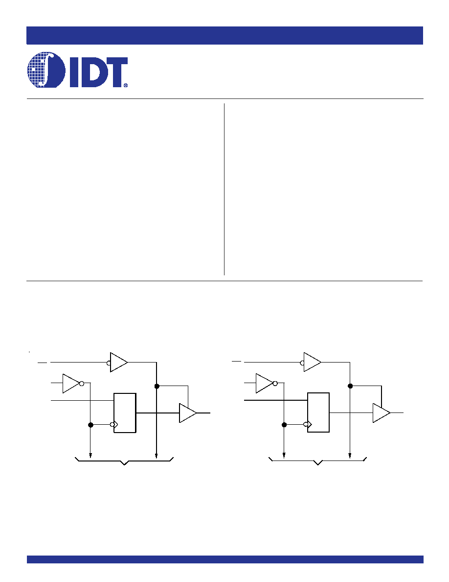
FUNCTIONAL BLOCK DIAGRAM
IDT74FCT163374A/C
3.3V CMOS 16-BIT
REGISTER (3-STATE)
DESCRIPTION:
The FCT163374 16-bit edge-triggered D-type register is built using
advanced dual metal CMOS technology. These high-speed, low-power
registers are ideal for use as buffer registers for data synchronization and
storage. The Output Enable (xOE) and clock (xCLK) controls are organized
to operate each device as two 8-bit registers or one 16-bit register with
common clock. Flow-through organization of signal pins facilitates ease of
layout. All inputs are designed with hysteresis for improved noise margin.
The inputs of FCT163374 can be driven from either 3.3V or 5V devices.
This feature allows the use of these devices as translators in a mixed 3.3V/
5V supply system.
2
O
1
2
OE
2
CLK
2
D
1
TO SEVEN OTHER CHANNELS
C
D
1
O
1
1
OE
1
CLK
1
D
1
TO SEVEN OTHER CHANNELS
C
D
24
25
36
2
13
1
48
47
2
INDUSTRIAL TEMPERATURE RANGE
IDT74FCT163374A/C
3.3V CMOS 16-BIT REGISTER (3-STATE)
Symbol
Description
Max
Unit
V
TERM
(2)
Terminal Voltage with Respect to GND
≠0.5 to +4.6
V
V
TERM
(3)
Terminal Voltage with Respect to GND
≠0.5 to 7
V
V
TERM
(4)
Terminal Voltage with Respect to GND
≠0.5 to V
CC
+0.5
V
T
STG
Storage Temperature
≠65 to +150
∞C
I
OUT
DC Output Current
≠60 to +60
mA
ABSOLUTE MAXIMUM RATINGS
(1)
NOTES:
1. Stresses greater than those listed under ABSOLUTE MAXIMUM RATINGS may cause
permanent damage to the device. This is a stress rating only and functional operation
of the device at these or any other conditions above those indicated in the operational
sections of this specification is not implied. Exposure to absolute maximum rating
conditions for extended periods may affect reliability.
2. Vcc terminals.
3. Input terminals.
4. Outputs and I/O terminals.
Symbol
Parameter
(1)
Conditions
Typ.
Max.
Unit
C
IN
Input Capacitance
V
IN
= 0V
3.5
6
pF
C
OUT
Output Capacitance
V
OUT
= 0V
3.5
8
pF
CAPACITANCE
(T
A
= +25∞C, F = 1.0MHz)
NOTE:
1. This parameter is measured at characterization but not tested.
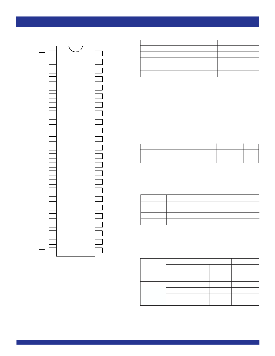
PIN CONFIGURATION
SSOP/ TSSOP/ TVSOP
TOP VIEW
Pin Names
Description
xDx
Data Inputs
xCLK
Clock Inputs
xOx
3-State Outputs
xOE
3-State Output Enable Input (Active LOW)
PIN DESCRIPTION
FUNCTION TABLE
(1)
Inputs
Outputs
Function
xDx
xCLK
xOE
xOx
Hi-Z
X
L
H
Z
X
H
H
Z
Load Register
L
L
L
H
L
H
L
H
Z
H
H
Z
NOTE:
1. H = HIGH Voltage Level
L = LOW Voltage Level
X = Don't Care
Z = High-Impedance
= LOW-to-HIGH transition
1
O
1
GND
1
O
3
V
CC
1
OE
GND
2
O
2
GND
V
CC
GND
1
O
2
1
O
4
1
O
5
1
O
6
1
O
7
1
O
8
2
O
1
2
O
3
2
O
4
2
O
5
2
O
7
2
O
8
2
O
6
2
OE
1
CLK
1
D
1
1
D
2
GND
1
D
3
1
D
4
V
CC
1
D
5
1
D
6
1
D
7
1
D
8
2
D
1
2
D
2
2
D
3
2
D
4
V
CC
2
D
5
2
D
7
2
D
8
2
D
6
2
CLK
GND
GND
GND
39
29
30
31
32
33
34
35
36
37
38
25
26
27
28
48
47
41
42
43
44
45
46
40
1
2
3
4
5
6
7
8
9
10
12
13
14
15
16
17
18
19
20
11
21
22
23
24
3
IDT74FCT163374A/C
3.3V CMOS 16-BIT REGISTER (3-STATE)
INDUSTRIAL TEMPERATURE RANGE
Symbol
Parameter
Test Conditions
(1)
Min.
Typ.
(2)
Max.
Unit
V
IH
Input HIGH Level (Input pins)
Guaranteed Logic HIGH Level
2
--
5.5
V
Input HIGH Level (I/O pins)
2
--
V
CC
+0.5
V
IL
Input LOW Level (Input and I/O pins) Guaranteed Logic LOW Level
≠0.5
--
0.8
V
I
IH
Input HIGH Current (Input pins)
V
CC
= Max.
V
I
= 5.5V
--
--
±1
Input HIGH Current (I/O pins)
V
I
= V
CC
--
--
±1
µA
I
IL
Input LOW Current (Input pins)
V
I
= GND
--
--
±1
Input LOW Current (I/O pins)
V
I
= GND
--
--
±1
I
OZH
High Impedance Output Current
V
CC
= Max.
V
O
= V
CC
--
--
±1
µA
I
OZL
(3-State Output pins)
V
O
= GND
--
--
±1
V
IK
Clamp Diode Voltage
V
CC
= Min., I
IN
= ≠18mA
--
≠0.7
≠1.2
V
I
ODH
Output HIGH Current
V
CC
= 3.3V, V
IN
= V
IH
or V
IL,
V
O
= 1.5V
(3)
≠36
≠60
≠110
mA
I
ODL
Output LOW Current
V
CC
= 3.3V, V
IN
= V
IH
or V
IL,
V
O
= 1.5V
(3)
50
90
200
mA
V
OH
Output HIGH Voltage
V
CC
= Min.
I
OH
= ≠0.1mA
V
CC
-0.2
--
--
V
IN
= V
IH
or V
IL
I
OH
= ≠3mA
2.4
3
--
V
V
CC
= 3V
I
OH
= ≠8mA
2.4
(5)
3
--
V
IN
= V
IH
or V
IL
V
OL
Output LOW Voltage
V
CC
= Min.
I
OL
= 0.1mA
--
--
0.2
V
IN
= V
IH
or V
IL
I
OL
= 16mA
--
0.2
0.4
I
OL
= 24mA
--
0.3
0.55
V
V
CC
= 3V
I
OL
= 24mA
--
0.3
0.5
V
IN
= V
IH
or V
IL
I
OS
Short Circuit Current
(4)
V
CC
= Max., V
O
= GND
(3)
≠60
≠135
≠240
mA
V
H
Input Hysteresis
--
--
150
--
mV
I
CCL
Quiescent Power Supply Current
V
CC
= Max.
--
0.1
10
µA
I
CCH
V
IN
= GND or V
CC
I
CCZ
DC ELECTRICAL CHARACTERISTICS OVER OPERATING RANGE
Following Conditions Apply Unless Otherwise Specified:
Industrial: T
A
= ≠40∞C to +85∞C, V
CC
= 2.7V to 3.6V
NOTES:
1. For conditions shown as Min. or Max., use appropriate value specified under Electrical Characteristics for the applicable device type.
2. Typical values are at V
CC
= 3.3V, +25∞C ambient.
3. Not more than one output should be shorted at one time. Duration of the test should not exceed one second.
4. This parameter is guaranteed but not tested.
5. V
OH
= V
CC
≠0.6V at rated current.
4
INDUSTRIAL TEMPERATURE RANGE
IDT74FCT163374A/C
3.3V CMOS 16-BIT REGISTER (3-STATE)
POWER SUPPLY CHARACTERISTICS
Symbol
Parameter
Test Conditions
(1)
Min.
Typ.
(2)
Max.
Unit
I
CC
Quiescent Power Supply
V
CC
= Max.
--
2
30
µA
Current TTL Inputs HIGH
V
IN
= V
CC
≠0.6V
(3)
I
CCD
Dynamic Power Supply Current
(4)
V
CC
= Max.
V
IN
= V
CC
--
50
75
µA/
Outputs Open
V
IN
= GND
MHz
xOE = GND
One Input Toggling
50% Duty Cycle
I
C
Total Power Supply Current
(6)
V
CC
= Max., Outputs Open
V
IN
= V
CC
--
0.5
0.8
mA
f
CP
= 10MHz
V
IN
= GND
50% Duty Cycle
xOE = GND
f
i
= 5MHz
V
IN
= V
CC
≠0.6V
--
0.5
0.8
One Bit Toggling
V
IN
= GND
V
CC
= Max., Outputs Open
V
IN
= V
CC
--
2.5
3.8
(5)
f
CP
= 10MHz
V
IN
= GND
50% Duty Cycle
xOE = GND
V
IN
= V
CC
≠0.6V
--
2.5
4
(5)
f
i
= 2.5MHz
V
IN
= GND
Sixteen Bits Toggling
NOTES:
1. For conditions shown as max. or min., use appropriate value specified under Electrical Characteristics for the applicable device type.
2. Typical values are at V
CC
= 3.3V, +25∞C ambient.
3. Per TTL driven input; all other inputs at V
CC
or GND.
4. This parameter is not directly testable, but is derived for use in Total Power Supply Calculations.
5. Values for these conditions are examples of the I
CC
formula. These limits are guaranteed but not tested.
6. I
C
= I
QUIESCENT
+ I
INPUTS
+ I
DYNAMIC
I
C
= I
CC
+ DI
CC
D
H
N
T
+ I
CCD
(f
CP
N
CP
/2 + fiNi)
I
CC
= Quiescent Current (I
CCL,
I
CCH
and
I
CCZ
)
I
CC
= Power Supply Current for a TTL High Input
D
H
= Duty Cycle for TTL Inputs High
N
T
= Number of TTL Inputs at D
H
I
CCD
= Dynamic Current Caused by an Input Transition Pair (HLH or LHL)
f
CP
= Clock Frequency for Register Devices (Zero for Non-Register Devices)
N
CP
= Number of Clock Inputs at f
CP
f
i
= Input Frequency
N
i
= Number of Inputs at fi
5
IDT74FCT163374A/C
3.3V CMOS 16-BIT REGISTER (3-STATE)
INDUSTRIAL TEMPERATURE RANGE
FCT163374A
FCT163374C
Symbol
Parameter
Condition
(2)
Min.
(3)
Max.
Min.
(3)
Max.
Unit
t
PLH
Propagation Delay
C
L
= 50pF
2
6.5
2
5.2
ns
t
PHL
xCLK to xOx
R
L
= 500
t
PZH
Output Enable Time
1.5
6.5
1.5
5.5
ns
t
PZL
t
PHZ
Output Disable Time
1.5
5.5
1.5
5
ns
t
PLZ
t
SU
Set-up Time HIGH or LOW, xDx to xCLK
2
--
2
--
ns
t
H
Hold Time HIGH or LOW, xDx to xCLK
1.5
--
1.5
--
ns
t
W
xCLK Pulse Width HIGH
5
--
5
--
ns
t
SK
(o)
Output Skew
(4)
--
0.5
--
0.5
ns
SWITCHING CHARACTERISTICS OVER OPERATING RANGE
(1)
NOTES:
1. Propagation Delays and Enable/Disable times are with V
CC
= 3.3V ±0.3V, Normal Range. For V
CC
= 2.7V to 3.6V, Extended Range, all Propagation Delays and Enable/Disable
times should be degraded by 20%.
2. See test circuit and waveforms.
3. Minimum limits are guaranteed but not tested on Propagation Delays.
4. Skew between any two outputs, of the same package, switching in the same direction. This parameter is guaranteed by design.
6
INDUSTRIAL TEMPERATURE RANGE
IDT74FCT163374A/C
3.3V CMOS 16-BIT REGISTER (3-STATE)
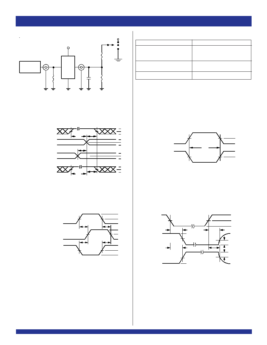
Pulse
Generator
R
T
D.U.T.
V
CC
V
IN
C
L
V
OUT
50pF
500
500
Open
GND
6v
3V
1.5V
0V
3V
1.5V
0V
3V
1.5V
0V
3V
1.5V
0V
DATA
INPUT
TIMING
INPUT
ASYNCHRONOUS CONTROL
PRESET
CLEAR
ETC.
SYNCHRONOUS CONTROL
t
SU
t
H
t
REM
t
SU
t
H
PRESET
CLEAR
CLOCK ENABLE
ETC.
HIGH-LOW-HIGH
PULSE
LOW-HIGH-LOW
PULSE
t
W
1.5V
1.5V
SAME PHASE
INPUT TRANSITION
3V
1.5V
0V
1.5V
V
OH
t
PLH
OUTPUT
OPPOSITE PHASE
INPUT TRANSITION
3V
1.5V
0V
t
PLH
t
PHL
t
PHL
V
OL
CONTROL
INPUT
3V
1.5V
0V
3V
0V
OUTPUT
NORMALLY
LOW
OUTPUT
NORMALLY
HIGH
SWITCH
6V
SWITCH
GND
V
OL
0.3V
0.3V
t
PLZ
t
PZL
t
PZH
t
PHZ
3V
0V
1.5V
1.5V
ENABLE
DISABLE
V
OH
TEST CIRCUITS AND WAVEFORMS
Propagation Delay
Test Circuits for All Outputs
Enable and Disable Times
Set-up, Hold, and Release Times
Pulse Width
Test
Switch
Open Drain
Disable Low
6V
Enable Low
Disable High
GND
Enable High
All Other Tests
Open
SWITCH POSITION
DEFINITIONS:
C
L
= Load capacitance: includes jig and probe capacitance.
R
T
= Termination resistance: should be equal to Z
OUT
of the Pulse Generator.
NOTES:
1. Diagram shown for input Control Enable-LOW and input Control Disable-HIGH.
2. Pulse Generator for All Pulses: Rate
1.0MHz; t
F
2.5ns; t
R
2.5ns.
3. if V
CC
is below 3V, input voltage swings should be adjusted not to exceed V
CC
.
7
IDT74FCT163374A/C
3.3V CMOS 16-BIT REGISTER (3-STATE)
INDUSTRIAL TEMPERATURE RANGE
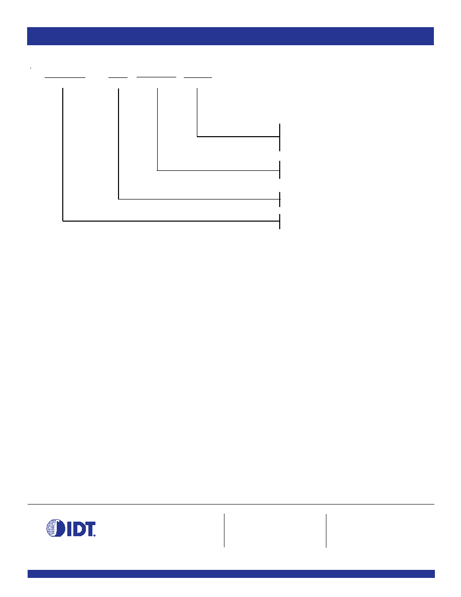
ORDERING INFORMATION
CORPORATE HEADQUARTERS
for SALES:
for Tech Support:
2975 Stender Way
800-345-7015 or 408-727-6116
logichelp@idt.com
Santa Clara, CA 95054
fax: 408-492-8674
(408) 654-6459
www.idt.com
4/22/2002 Removed blank speed grade
DATA SHEET DOCUMENT HISTORY
XX
Temp. Range
XXXX
Device Type
X
Package
PV
PA
PF
Shrink Small Outline Package
Thin Shrink Small Outline Package
Thin Very Small Outline Package
- 40∞C to +85∞C
74
IDT
FCT
XXX
Family
163
Double-Density 3.3Volt
374A
374C
Non-Inverting 16-Bit Register