1
IDT74FCT16827AT/CT
FAST CMOS 20-BIT BUFFER
INDUSTRIAL TEMPERATURE RANGE
JUNE 2002
IDT74FCT16827AT/CT
INDUSTRIAL TEMPERATURE RANGE
FAST CMOS
20-BIT BUFFER
DESCRIPTION:
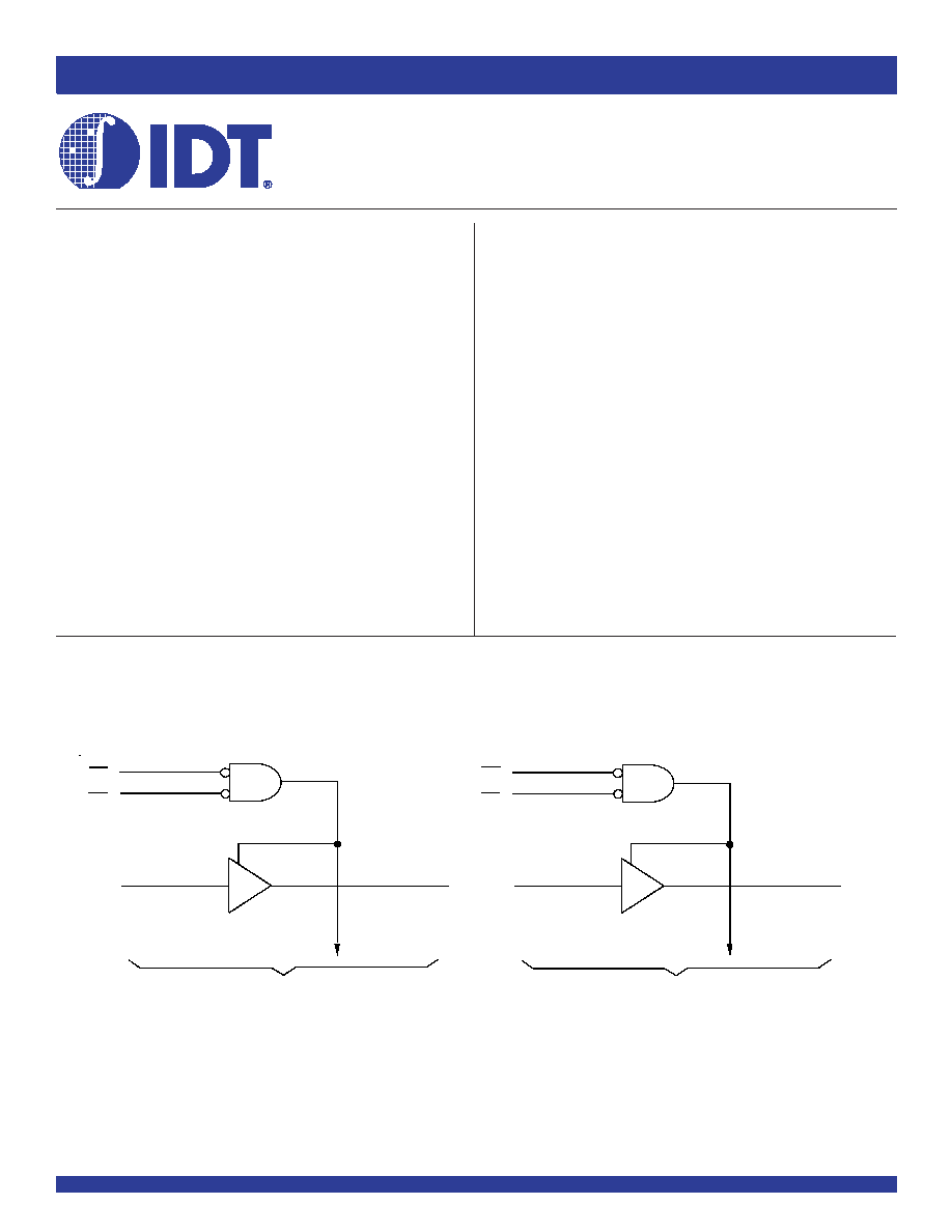
The FCT16827T 20-bit buffer is built using advanced dual metal CMOS
technology. These 20-bit bus drivers provide high-performance bus interface
buffering for wide data/address paths or buses carrying parity. Two pair of
NAND-ed output enable controls offer maximum control flexibility and are
organized to operate the device as two 10-bit buffers or one 20-bit buffer. Flow-
through organization of signal pins simplifies layout. All inputs are designed with
hysteresis for improved noise margin.
The FCT16827T is ideally suited for driving high capacitance loads and low
impedance backplanes. The output buffers are designed with power off disable
capability to allow "live insertion" of boards when used as backplane drivers.
2
Y
1
TO NINE O THER CHANNELS
2
O E
1
2
OE
2
2
A
1
1
Y
1
TO NINE O THER CHANNELS
1
OE
1
1
O E
2
1
A
1
1
56
55
28
29
42
2
15
FEATURES:
∑ 0.5 MICRON CMOS Technology
∑ High-speed, low-power CMOS replacement for ABT functions
∑ Typical t
SK(o)
(Output Skew) < 250ps
∑ Low input and output leakage
1µA (max.)
∑ V
CC
= 5V ±10%
∑ High drive outputs (≠32mA I
OH
, 64mA I
OL
)
∑ Power off disable outputs permit "live insertion"
∑ Typical V
OLP
(Output Ground Bounce) < 1.0V at V
CC
= 5V,
T
A
= 25∞C
∑ Available in SSOP and TSSOP packages
FUNCTIONAL BLOCK DIAGRAM
The IDT logo is a registered trademark of Integrated Device Technology, Inc.
© 2002 Integrated Device Technology, Inc.
DSC-5439/1

2
INDUSTRIAL TEMPERATURE RANGE
IDT74FCT16827AT/CT
FAST CMOS 20-BIT BUFFER
SSOP/ TSSOP
TOP VIEW
PIN CONFIGURATION
1
Y
1
GND
1
Y
3
V
CC
1
OE
1
GND
1
Y
10
GND
1
Y
2
1
Y
4
1
Y
5
1
Y
6
1
Y
7
1
Y
8
1
Y
9
2
Y
3
V
CC
GND
2
Y
4
2
Y
5
2
Y
7
2
Y
8
2
Y
6
2
OE
1
1
OE
2
1
A
1
1
A
2
GND
1
A
3
1
A
4
V
CC
1
A
5
1
A
6
1
A
7
1
A
8
1
A
9
1
A
10
GND
GND
47
37
38
39
40
41
42
43
44
45
46
33
34
35
36
56
55
49
50
51
52
53
54
48
1
2
3
4
5
6
7
8
9
10
12
13
14
15
16
17
18
19
20
11
21
22
23
24
2
Y
1
2
Y
2
2
Y
10
2
Y
9
2
A
3
2
A
4
V
CC
2
A
5
2
A
7
2
A
8
2
A
6
GND
2
A
9
2
A
10
2
OE
2
29
30
31
32
25
26
27
28
2
A
1
2
A
2
Symbol
Description
Max
Unit
V
TERM(2)
Terminal Voltage with Respect to GND
≠0.5 to +7
V
V
TERM(3)
Terminal Voltage with Respect to GND
≠0.5 to V
CC
+0.5
V
T
STG
Storage Temperature
≠65 to +150
∞C
I
OUT
DC Output Current
≠60 to +120
mA
ABSOLUTE MAXIMUM RATINGS
(1)
NOTES:
1. Stresses greater than those listed under ABSOLUTE MAXIMUM RATINGS may cause
permanent damage to the device. This is a stress rating only and functional operation
of the device at these or any other conditions above those indicated in the operational
sections of this specification is not implied. Exposure to absolute maximum rating
conditions for extended periods may affect reliability.
2. All device terminals except FCT162XXX Output and I/O terminals.
3. Outputs and I/O terminals for FCT162XXX.
Symbol
Parameter
(1)
Conditions
Typ.
Max.
Unit
C
IN
Input Capacitance
V
IN
= 0V
3.5
6
pF
C
OUT
Output Capacitance
V
OUT
= 0V
3.5
8
pF
CAPACITANCE
(T
A
= +25∞C, f = 1.0MHz)
NOTE:
1. This parameter is measured at characterization but not tested.
Pin Names
Description
xOEx
Output Enable Inputs (Active LOW)
xAx
Data Inputs
xYx
3-State Outputs
PIN DESCRIPTION
Inputs
Outputs
xOE
1
xOE
2
xAx
xYx
L
L
L
L
L
L
H
H
H
X
X
Z
X
H
X
Z
FUNCTION TABLE
(1)
NOTE:
1. H = HIGH voltage level
L = LOW voltage level
X = Don't care
Z = High-Impedance
3
IDT74FCT16827AT/CT
FAST CMOS 20-BIT BUFFER
INDUSTRIAL TEMPERATURE RANGE
Symbol
Parameter
Test Conditions
(1)
Min.
Typ.
(2)
Max.
Unit
V
IH
Input HIGH Level
Guaranteed Logic HIGH Level
2
--
--
V
V
IL
Input LOW Level
Guaranteed Logic LOW Level
--
--
0.8
V
I
IH
Input HIGH Current (Input pins)
(5)
V
CC
= Max.
V
I
= V
CC
--
--
±1
µA
Input HIGH Current (I/O pins)
(5)
--
--
±1
I
IL
Input LOW Current (Input pins)
(5)
V
I
= GND
--
--
±1
Input LOW Current (I/O pins)
(5)
--
--
±1
I
OZH
High Impedance Output Current
V
CC
= Max.
V
O
= 2.7V
--
--
±1
µA
I
OZL
(3-State Output pins)
(5)
V
O
= 0.5V
--
--
±1
V
IK
Clamp Diode Voltage
V
CC
= Min., I
IN
= ≠18mA
--
≠0.7
≠1.2
V
I
OS
Short Circuit Current
V
CC
= Max., V
O
= GND
(3)
≠80
≠140
≠250
mA
V
H
Input Hysteresis
--
--
100
--
mV
I
CCL
Quiescent Power Supply Current
V
CC
= Max
--
5
500
µA
I
CCH
V
IN
= GND or V
CC
I
CCZ
DC ELECTRICAL CHARACTERISTICS OVER OPERATING RANGE
Following Conditions Apply Unless Otherwise Specified:
Industrial: T
A
= ≠40∞C to +85∞C, V
CC
= 5.0V ±10%
NOTES:
1. For conditions shown as Min. or Max., use appropriate value specified under Electrical Characteristics for the applicable device type.
2. Typical values are at V
CC
= 5.0V, +25∞C ambient.
3. Not more than one output should be shorted at one time. Duration of the test should not exceed one second.
4. Duration of the condition can not exceed one second.
5. This test limit for this parameter is ±5µA at T
A
= ≠55∞C.
Symbol
Parameter
Test Conditions
(1)
Min.
Typ.
(2)
Max.
Unit
I
O
Output Drive Current
V
CC
= Max.
,
V
O
= 2.5V
(3)
≠50
--
≠180
mA
V
OH
Output HIGH Voltage
V
CC
= Min.
I
OH
= ≠3mA
2.5
3.5
--
V
IN
= V
IH
or V
IL
I
OH
= ≠15mA
2.4
3.5
--
V
I
OH
= ≠32mA
(4)
2
3
--
V
OL
Output LOW Voltage
V
CC
= Min.
I
OL
= 64mA
--
0.2
0.55
V
V
IN
= V
IH
or V
IL
I
OFF
Input/Output Power Off Leakage
(5)
V
CC
= 0V, V
IN
or V
O
4.5V
--
--
±1
µA
OUTPUT DRIVE CHARACTERISTICS
4
INDUSTRIAL TEMPERATURE RANGE
IDT74FCT16827AT/CT
FAST CMOS 20-BIT BUFFER
Symbol
Parameter
Test Conditions
(1)
Min.
Typ.
(2)
Max.
Unit
I
CC
Quiescent Power Supply Current
V
CC
= Max.
--
0.5
1.5
mA
TTL Inputs HIGH
V
IN
= 3.4V
(3)
I
CCD
Dynamic Power Supply Current
(4)
V
CC
= Max.
V
IN
= V
CC
--
60
100
µA/
Outputs Open
V
IN
= GND
MHz
xOE
1
= xOE
2
= GND
One Input Toggling
50% Duty Cycle
I
C
Total Power Supply Current
(6)
V
CC
= Max.
V
IN
= V
CC
--
0.6
1.5
mA
Outputs Open
V
IN
= GND
fi = 10MHz
50% Duty Cycle
V
IN
= 3.4V
--
0.9
2.3
xOE
1
= xOE
2
= GND
V
IN
= GND
One Bit Toggling
V
CC
= Max.
V
IN
= V
CC
--
3
5.5
(5)
Outputs Open
V
IN
= GND
fi
= 2.5MHz
50% Duty Cycle
V
IN
= 3.4V
--
8
20.5
(5)
xOE
1
= xOE
2
= GND
V
IN
= GND
Twenty Bits Toggling
NOTES:
1. For conditions shown as Min. or Max., use appropriate value specified under Electrical Characteristics for the applicable device type.
2. Typical values are at V
CC
= 5.0V, +25∞C ambient.
3. Per TTL driven input (V
IN
= 3.4V). All other inputs at V
CC
or GND.
4. This parameter is not directly testable, but is derived for use in Total Power Supply Calculations.
5. Values for these conditions are examples of the I
CC
formula. These limits are guaranteed but not tested.
6. I
C
= I
QUIESCENT
+ I
INPUTS
+ I
DYNAMIC
I
C
= I
CC
+
I
CC
D
H
N
T
+ I
CCD
(f
CP
N
CP
/2 + fiNi)
I
CC
= Quiescent Current (I
CCL
, I
CCH
and I
CCZ
)
I
CC
= Power Supply Current for a TTL High Input (V
IN
= 3.4V)
D
H
= Duty Cycle for TTL Inputs High
N
T
= Number of TTL Inputs at D
H
I
CCD
= Dynamic Current Caused by an Input Transition Pair (HLH or LHL)
f
CP
= Clock Frequency for Register Devices (Zero for Non-Register Devices)
N
CP
= Number of Clock Inputs at f
CP
f
i
= Input Frequency
N
i
= Number of Inputs at f
i
POWER SUPPLY CHARACTERISTICS
5
IDT74FCT16827AT/CT
FAST CMOS 20-BIT BUFFER
INDUSTRIAL TEMPERATURE RANGE
74FCT16827AT
74FCT16827CT
Symbol
Parameter
Condition
(1)
Min.
(2)
Max.
Min.
(2)
Max.
Unit
t
PLH
Propagation Delay
C
L
= 50pF
1.5
8
1.5
3.7
ns
t
PHL
xAx to xYx
R
L
= 500
C
L
= 300pF
(3)
1.5
15
1.5
7
R
L
= 500
t
PZH
Output Enable Time
C
L
= 50pF
1.5
12
1.5
4.8
ns
t
PZL
xOEx to xYx
R
L
= 500
C
L
= 300pF
(3)
1.5
23
1.5
9
R
L
= 500
t
PZH
Output Disable Time
C
L
= 5pF
(3)
1.5
9
1.5
4
ns
t
PZL
xOEx to xYx
R
L
= 500
C
L
= 50pF
1.5
10
1.5
4
R
L
= 500
t
SK(o)
Output Skew
(4)
--
0.5
--
0.5
ns
SWITCHING CHARACTERISTICS OVER OPERATING RANGE
NOTES:
1. See test circuit and waveforms.
2. Minimum limits are guaranteed but not tested on Propagation Delays.
3. This limit is guaranteed but not tested.
4. Skew between any two outputs, of the same package, switching in the same direction. This parameter is guaranteed by design.
6
INDUSTRIAL TEMPERATURE RANGE
IDT74FCT16827AT/CT
FAST CMOS 20-BIT BUFFER
Pulse
Generator
R
T
D.U.T.
V
CC
V
IN
C
L
V
OUT
50pF
500
500
7.0V
3V
1.5V
0V
3V
1.5V
0V
3V
1.5V
0V
3V
1.5V
0V
D ATA
INPUT
TIM IN G
INPUT
ASYNC HR ONOUS C ONTROL
PRES ET
CLEA R
ETC .
SYNCHR ON OUS CONTROL
t
SU
t
H
t
R EM
t
SU
t
H
PRES ET
CLEA R
CLOCK ENABLE
ETC .
HIGH-LOW -H IGH
PU LSE
LOW -HIGH-LOW
PU LSE
t
W
1.5V
1.5V
SAM E PHASE
INPUT TRAN SITION
3V
1.5V
0V
1.5V
V
O H
t
PLH
OU TPU T
OPPOSITE P HASE
INPUT TRAN SITION
3V
1.5V
0V
t
PL H
t
PH L
t
PH L
V
O L
CONTROL
IN PU T
3V
1.5V
0V
3.5V
0V
OUTPU T
NORM ALLY
LOW
OUTPU T
NORM ALLY
H IGH
SW ITCH
C LOSE D
SW ITC H
OPEN
V
OL
0.3V
0.3V
t
PLZ
t
PZL
t
PZH
t
PHZ
3.5V
0V
1.5V
1.5V
ENABLE
D ISABLE
V
OH
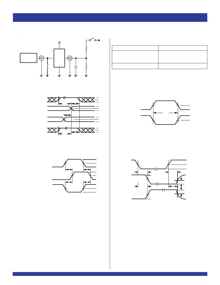
TEST CIRCUITS AND WAVEFORMS
Propagation Delay
Test Circuits for All Outputs
Enable and Disable Times
Set-up, Hold, and Release Times
Pulse Width
NOTES:
1. Diagram shown for input Control Enable-LOW and input Control Disable-HIGH.
2. Pulse Generator for All Pulses: Rate
1.0MHz; t
F
2.5ns; t
R
2.5ns.
Test
Switch
Open Drain
Disable Low
Closed
Enable Low
All Other Tests
Open
SWITCH POSITION
DEFINITIONS:
C
L
= Load capacitance: includes jig and probe capacitance.
R
T
= Termination resistance: should be equal to Z
OUT
of the Pulse Generator.
7
IDT74FCT16827AT/CT
FAST CMOS 20-BIT BUFFER
INDUSTRIAL TEMPERATURE RANGE
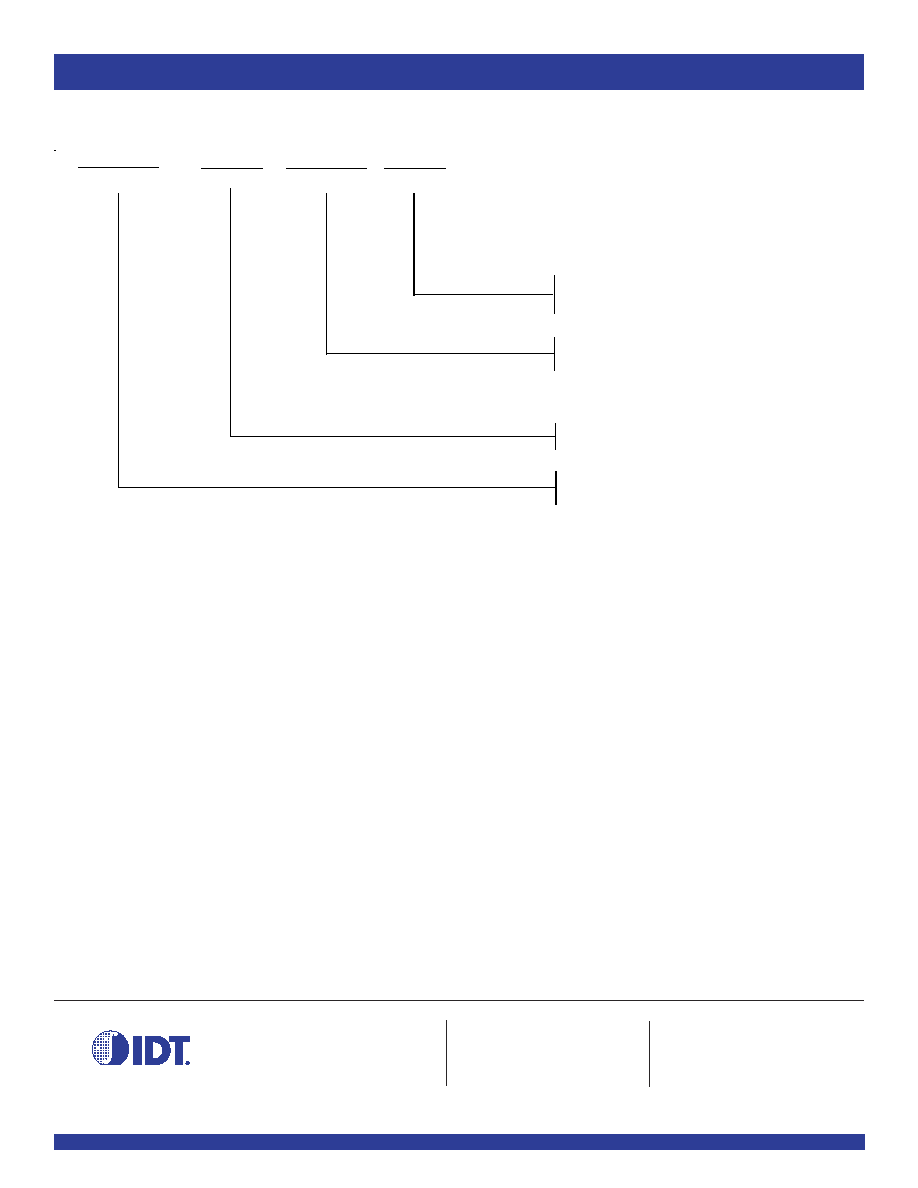
ORDERING INFORMATION
IDT XX
Temp. Range
XXXX
Device Type
XX
Package
PV
PA
Shrink Small Outline Package
Thin Shrink Small Outline Package
20-Bit Buffer
74
≠ 40∞C to +85∞C
16
Double-Density, 5 Volt, High Drive
FCT
XXX
Family
827AT
827CT
CORPORATE HEADQUARTERS
for SALES:
for Tech Support:
2975 Stender Way
800-345-7015 or 408-727-6116
logichelp@idt.com
Santa Clara, CA 95054
fax: 408-492-8674
(408) 654-6459
www.idt.com
5/21/2002 Removed TVSOP package
6/21/2002 Updated as per PDNs Logic-00-07 and Logic-01-04
DATA SHEET DOCUMENT HISTORY